DRAM is a volatile memory since information stored is destroyed once the power supply to it stops even for a short duration. Information is also lost because of charge leakage from the storage capacitor unless it is periodically charged or refreshed. In spite of this complexity of operation and comparatively larger data access time with respect to SRAM, DRAMs have been produced in largest quantities because of their low cost per bit [1]. There are quite a few reasons for the low cost of DRAM memory. Prominent among the reasons is the changeover from 6/4 transistor SRAM to 3 transistor DRAM and eventually to single-transistor–single-capacitor DRAM. Consumed chip area per bit further continued to reduce on account of reduction in design rules. Obviously smaller cell size fabrication could become possible only with the advancements in technology at each generation. However, circuit innovations and advancements connected with DRAMs were no less important. At the earliest stages, it was the deployment of sense amplifiers that not only improved performance of the DRAM but also ensured its functionality. A brief mention of the same is included in Section 3.2 and in some detail in Chapter 8. Section 3.2.1 includes the importance of conversion to mixed NMOS/CMOS from the pure NMOS DRAMs, which also facilitated half-VDD precharge of bit-line technique. It resulted in great boost to the DRAM deployment with reduced power consumption. Initially planar DRAM cell was simple in realization with a planar capacitor and the access transistor placed side by side. It continued up to nearly 4 Mbit DRAM density level but beyond that technology had to change to three-dimensional realization of capacitor with adoption of Si3N4 and Ta2O5 dielectrics. At the same time sensing techniques were improved for the detection of small signals during read operation. Some other features, like use of redundancy and folded bit line architecture, were also important developments at this stage. Main technological developments for 16 Mbit to 1 Gbit DRAM range have been discussed in Section 3.4. One major concern of obtaining ~25 fF capacitance in as small chip area as possible is also discussed. Though its advanced technology is described in Chapter 5, Sections 3.4.1 and 3.4.2 discuss new capacitances in metal insulator-metal (MIM) form especially in CROWN shape and those using higher-dielectric material like Ta2O5. Capacitor-over-bit-line (COB) type of DRAM cell, a special form of a cell that was only briefly mentioned with other kinds of DRAM cells in Chapter 2, is now taken up in some detail in Section 3.5.
3.2 DRAM Technology—Early Stage Development
In 1972, Intel manufactured a 1 Kbit DRAM chip commercially. This chip had 32 rows and columns each, and every intersection had a silicon-gate p-channel type cell having three MOS transistors. Refreshing was done every 2 ms and the chip worked on supply voltage of −17 V with +3 V biasing of the n-type substrate and the p-type source [2]. Soon an n-channel 4 Kbit DRAM was manufactured at 10 μm feature size, using a three-transistor cell with single-polysilicon, single aluminum metallization scheme.
Changeover from three transistors to one transistor cell was an extremely important development as it considerably improved the cell density. One transistor cell became almost universal for fabricating DRAMs up to the highest density level. Though 4 Kbit DRAM cell would become industry standard in 1973 [3], it was Dennard’s patent of 1968 [4] which gave first memory cell using only one transistor. One of the major problems of detecting small cell signal was soon solved by the use of a differential amplifier in the middle of the bit line called a sense amplifier, which structurally divided the bit line in two halves [5]; it automatically restored/refreshed the cell as well. The first commercial product using one transistor DRAM cell with gated flip-flop sense amplifier was at 4 Kbit level produced by Texas Instruments using power supply of 12 V with −3 V substrate bias. A very important development reported in 1973 and which was converted to reality in 1975 was address multiplexing [6], again at the 4 Kbit level. A row address strobe (RAS) first selects all the cells in a row, and activates sense amplifiers. Then column address strobe (CAS) was applied to select a desired cell and the sensing signal is detected by the sense amplifier for reading or data is made available through I/O bus for writing. As RAS strobe selected all cells in a row, RAS only refresh became standard due to multiplexing. A page of data term was also coined for the cells of a row and later used for rapid page mode reading of memory.
A 16 Kbit DRAM created by Proebsting became the industry standard [7], and it was the 16 Kbit generation which used 12 V, +5 V, and −5 V supplies before the next generation of 64 Kbit DRAMs, which used only 5 V supply—an important development. Beyond 16 Kbit, development was mainly through scaling down cell dimensions. However, decrease in the size of the access transistor, and storage capacitor, and reduction in the power supply to 5 V, necessitated the development of better sensitivity sense amplifiers. A number of modifications/improvements were made on the basic gated flip-flop sense amplifier including use of dummy cell as a reference. One important improvement in the sense amplifier design came in the form of charge-transfer cross-coupled circuit, which could sense smaller signals and was also useful in minimizing the problem of threshold mismatch of driver transistors of the sense amplifier [8]. Another important development was the word line boost by at least a threshold voltage above the new standard 5 V supply to compensate the back gate effect of the source to substrate potential.
As mentioned, the sense amplifier was placed in the middle, which divided the bit line in equal halves in the open bit-line structure. In this structure noise generated on two sides of the sense amplifier was unbalanced. There were many more reasons for the noise generation, like imbalance of the sense amplifier, transistor threshold difference due to the process variations, noise generated in nearby peripheral circuits, and also a considerable noise due to capacitive coupling between the bit line and word line. At 4 to 64 Kbit DRAM level, folded bit-line architecture was used in which the bit line itself was folded back, forming a pair, and the sense amplifier was placed at the end. It eliminated the common mode noise generated on the column decoders. Folded bit line arrangement also had the advantage of simpler bit line shorting for precharge and provided simpler column access.
The 256 Kbit DRAM generation was the stage when early CMOS DRAM was manufactured, but NMOS DRAMs were equally important. Folded bit line did show improvements in noise reduction, but open bit line was also used in good amount. In the mixed NMOS/CMOS technology the access transistor and storage capacitor were normally fabricated in the NMOS technology and the peripheral circuits in CMOS technology. Apart from the well-known advantage of lower power consumption, CMOS design improved refresh characteristics in comparison to NMOS design mainly because of providing restriction on thermally generated charges from substrate defects close to the memory cells. Access time in CMOS design could also be reduced by using static column decoding, which was better suited than NMOS design.
In spite of significant advantages of CMOS technology, some teething trouble stalled the full development of CMOS processing till 1 Mbit generation. From the functionality point of view, latch-up could occur because of noises and parasitics, leading to malfunctioning or even breakdown. However, a major problem was the rising cost in terms of increase in the number of masks and processing steps. Biasing of substrate was found to be useful in minimizing latch-up by reducing minority carrier injection. At the same time prohibitively high power consumption per bit level for high density DRAMs forced minimal use of NMOS technology. When the memory capacity increased from 1 Mbit to 64 Mbit die size increased from 5 × 10 mm2 to 12.7 × 20.4 mm2. The word line and bit line lengths increased in higher density DRAMs which increased their resistance and capacitance and hence resulted in (1) increased delay associated with the charging and discharging of these lines, and (2) the sensing signal in the bit line reduced in direct proportion as it depended on the ratio of storage cell capacitance to bit line capacitance. It necessitated development of better sensing methods and better sense amplifier [9]. With DRAM density reaching 1 Mb, planar storage capacitors were employed and trench and stacked capacitor were becoming necessities for reducing the die size and retaining sufficient charge on the storage capacitor with even smaller size. Boosting the word line was a standard approach at +5 V supply voltage level. However, in this approach some of the nodes needed observation where greater voltage level was likely to pose problems. Although this was not a major issue with feature size used at 1 Mbit level, it came into focus at latter stage with further reduced channel length. A pumped supply level set by feedback control was employed for the word line driver as a better solution in place of double bootstrap voltages [10]; the approach was successful at 4 Mbit level as well. However, big boost to CMOS came in the form of half-VDD bit line sensing with n-well CMOS DRAMs in 1984 [11] giving a number of advantages. More details were given in Chapter 2.
Another important feature of CMOS DRAM was the introduction of redundancy at 256 Kbit level, that is, use of additional rows and columns available for replacing defective ones for improving the memory yield through error correction circuits. The system came to be universally adopted with modifications and improvements and shall be discussed a little more in Chapter 8.
From 16 Kbit to 1 Mbit density level mostly a double-poly planar cell was used. However, for higher-density DRAMs, area occupied by this two-dimensional capacitor crossed a limit where the simple structure was not affordable and three-dimensional capacitors like trench [12] and stacked capacitors [13] were used. A two-or three-dimensional sensing signal can be increased by reducing noise, bit line capacitance and storage capacitor dielectric thickness, and by increasing capacitor area, its dielectric strength and storage signal. In the trench capacitors, which were mostly used at the 4 Mbit level and beyond, capacitor area was increased by increasing the trench depth and the capacitor dielectric formed on the trench wall was made as thin as practically feasible. Thermally grown silicon dioxide and CVD silicon nitride composite dielectric films were used for capacitance enhancement and prevention of leakage due to oxide breakdown. The main problem with the trench capacitor is the difficulty in fabricating a deeper trench for further capacitance enhancement. Stacked capacitor was also used at the 4 Mbit level, but it was preferable over trench capacitor at higher density level because of its easier fabrication and being less prone to noise and soft errors. Composite SiO2/Si3N4 films were better than only SiO2, but beyond 16 Mbit, even the composite layer was not able to provide enough capacitance and practical limitations forced a search for other dielectrics. At 64 Mbit CROWN-type memory cell was produced using Ta2O5 film and at 256 Mbit density Ta2O5 as well as Ba0.5Sr0.5TiO3 [14] films were successfully used by the manufacturers.
Some of the features which helped consolidating the manufacture of 1 Mbit CMOS DRAM were better sense amplifiers, use of address transition detection and redundancy, and suppression of noise through the folded bit line architecture, etc. At further increased DRAM density, storage capacitance was realized using trench or stacked capacitors but the DRAMs started to become slow on account of increased parasitic resistance and capacitance of almost unchanged number of cells connected to ever-thinning word and bit lines. Increased charging–discharging currents created reliability problems due to larger voltage drop in the word and bit lines. Apart from the established mentioned features of 1 Mbit density level new design techniques and changes in architecture were required for 4 Mbit and higher density level.
With continued reduction in feature size, smaller channel length of transistor made them susceptible to hot electrons at the then standard 5 V power supply. One of the solutions was to reduce voltage levels for the DRAM cell array using on-chip voltage converters. One such example at the early stage is the 16 Mbit DRAM given by Hitachi which used 3.3 V internal voltage for 0.6 μm MOS channel transistors [15], while peripheral circuits used +5 V supply with transistor channel length at 0.9 μm. However, reduced voltage required further improvement in bit line sensing and more reduction in noise, especially the bit-line coupling noise.
3.4 16 Mbit–256 Mbit, 1 Gbit DRAM Development
For realizing 64 Mbit DRAM, cell area must be less than 1.5 μm2. Because of the smallness of the cell area and intercell distance, trench capacitors have a tendency to suffer from leakage of charge, and lithographic limitation did not allow the fabrication of stacked capacitors like fin structure or cylindrical structure unless some relatively complex processing steps were taken. A comparatively planar topography is used in dual cell plate (DCP) stacked capacitor cells to overcome the lithographic limitations [16]. Planar area of the storage node is maximized by using data line shielded structure [17]. The storage node comprises two cubical parts of thick polysilicon and one cylindrical part of thin polysilicon, and the whole top and sidewalls of storage node are enclosed by top cell plates and the bottom side is covered by the lower cell plate to maximize the storage capacity as shown in Figure 2.21. For a cell having an area of 2.88 μm2, realized capacitance was about 50 fF with 5 nm thick dielectric and 600 nm thick storage polysilicon. In a 64 Mbit DRAM, for cell area to be less than 1.3 μm2, 0.3 μm technology was to be used; calculated capacitance became 25 fF with 5 nm (oxide-nitride-oxide) ONO dielectrics and 0.5 μm thick storage polysilicon. It is important to note that at 64 Mbit level or beyond, reliability of thin gate oxide became critical as the operating word line voltage was not scaled down with every DRAM generation, resulting in stress field across the gate oxide. Hence, time-dependent dielectric breakdown (TDDB), which is affected by the thinness of the gate oxide along with operating temperature and supply voltage, needed to be in check. It was observed that an ONO TDDB characteristic of the DCP cell is almost the same as that of a conventional stacked capacitor cell. Because of the inherent variations in oxide thickness during fabrication process and the operating temperature, degradations affect TDDB as well. Toshiba has given word line architecture for a 64 Mbit DRAM which could compensate for such degradations [18].
The preceding paragraph showed example of a 64 Mbit DRAM which emphasized achieving sufficient storage capacitance in a small projected chip area. At a working voltage of 3.3 V, and the kind of noise generation in early 1990s structures, 45 fF capacitor was essential for a 64 Mbit level DRAM so as to get satisfactory signal for sense amplifier and good soft-error immunity. Hence, a three-dimensional capacitor became essential which required enhanced photolithographic techniques, in addition to other improvements in fabrication processes. Getting higher value of cell capacitance also suggested the use of higher dielectric constant insulators like tantalum pentoxide (Ta2O5). It was not only the storage capacitor, but fabrication of reliable access transistor at around 0.35 μm technology with thin gate oxide and shallow junction depth at low thermal budget, also became a challenge.
3.4.1 Crown-Shaped Stacked Capacitor Cell Technology
An experimental 64 Mbit DRAM was fabricated in 0.3 μm technology, which was operated at a low voltage of 1.5 V and used a newly developed crown-shaped stacked capacitor [19]. In the CROWN cell, shown in Figure 2.24, a crown-shaped storage electrode combined with a smaller self-aligned cell structure produced a cell capacitance of 40 fF in a chip area of 1.28 μm2. A CROWN cell with a single wall crown-shaped electrode using a 3 nm equivalent CVD-Ta2O5 film with tungsten plate realized more than 40 fF capacitance, which was extendible to 70 fF for a double-wall CROWN structure. In the newly developed fabrication process for the CROWN cell, a planar WSi2 surface is obtained using etch-back method on polycrystalline surface, as shown in Figure 3.1, along with a nonplanarized structure. Planarization of WSi2 allows formation of low resistance (15Ω Sq.) data line on the word lines. The data lines are realized using anisotropic dry etching.
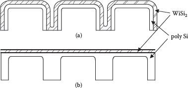
FIGURE 3.1
Structural comparison between (a) conventional nonplanarized data line, and (b) developed planarized data line. (Redrawn from “Crown-Shaped Stacked-Capacitor Cell for 1.5 V Operation 64-Mb DRAMs,” T. Kaga et al., IEEE Electr. Dev. Vol. 38, pp. 255–260, 1991.)
The crown-shaped storage node and the selective polycrystalline silicon contact formation is done through self-aligned process which requires highly selective anisotropic dry etching for the thick Si3N4 film. Hence, a CH2F2 plasma etching [20] was used which has high selective etching rate of ~40 between Si3N4 and SiO2 film. Despite the drawback of severe topography and requirement of large depth of focus from lithographic tools, CROWN structure using Ta2O5 dielectric has been shown to be the most promising candidate at 64/256 Mbit DRAM density level [21]. In the referred study, the conclusion is based on a comparison among a variety of 16 Mb/64 Mb DRAM structures on the basis of a figure of merit, “the ratio of the capacitor area to the cell area.”
An MIM crown-shaped capacitor has also been used to fabricate a 1 Gbit DRAM at 0.16 μm design rule, using 0.29 μm2 chip area [22]. Substituted tungsten (SW) electrode technology was developed in which electrode was formed substituting tungsten in place of polysilicon as shown in Figure 3.2. Shape and thickness of the electrode can easily be controlled in SW, which was not possible with polysilicon at smaller design rules. Another requirement at 0.16 μm technology was that of fine isolation. A single-Si3N4-spacer (SSS) offset local oxidation (OSELO), an improved version of OSELO II [23], was developed that reduced fabrication steps and provided better isolation than conventional structures. In STC-type cells, lithographic resolution becomes a problem because of the memory cell height. Even the use of recessed array (RA) technology [24] was not able to decrease the height difference sufficiently. Therefore, plate-wiring-merge (PWM) was introduced to decrease the height difference to about 0.5 μm, which was within the limits of the depth of focus in KrF-excimer phase-shift lithography.
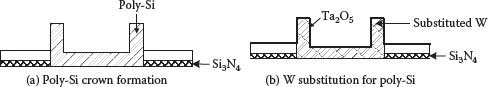
FIGURE 3.2
Substituted W electrode for Ta2 O5 CROWN capacitor. (Redrawn from “A.29 μm2 MIM-CROWN Cell and Process Technologies for 1 Gigabit DRAMs,” T. Kaga et al., IEDM Tech. Dig., pp. 927–929, 1994.)
A 64 Mbit DRAM using 1.28 μm2 crown-shaped stacked capacitor has been fabricated to work at low voltage of 1.5 V, while maintaining speed performance [25]. Better speed performance was obtained by using a complementary current-sensing scheme and a word line driver circuit, which allowed the data line voltage to swing to its full value. CROWN cell was found to be suitable at low voltage as data line interference noise is reduced due to the shielding of data lines by either the plate or storage layer.
Noise minimization/elimination has always been a priority item in DRAMs. Folded-bit line architecture was an important step in this direction, but it has limitations in typical cross-point cell memory arrays. A divided/shared bit line (DSB) scheme was developed at 64 Mbit levels for signal sensing, which eliminated common-mode noise [26]. In DSB scheme folded bit-line scheme is used in a cross-point cell arrangement, which not only eliminates common mode noise but also provides higher density. Inter-bit coupling noise was minimized through the use of a twisted bit line technique.
3.4.2 Tantalum Pentoxide (Ta2O5)–Based Storage Capacitor
DRAM density range of 64 Mbit to 1 Gbit saw a marked interest in the investigation and usage of high-density dielectrics especially tantalum pentoxide (Ta2O5) in place of SiO2 or ONO layers for storage capacitor [19,22,25,27,28,29,30,31,32,33,34]. At 64 Mbit level CROWN cell used a 3-nm equivalent CVD-Ta2O5 film to obtain 40 fF in a cell area of 1.28 μm2 [19,25]. However, reliability in Ta2O5 CVD technology was enhanced by Kamiyama and Saeki [31] by introducing some finer processing steps. Rapid thermal nitridation (RTN) of native SiO2 on the stacked poly-Si was done at 900°C for 60 sec in NH3 atmosphere, which helped in reducing the equivalent oxide thickness. After low-pressure CVD (LPCVD) Ta2O5 film deposition rapid thermal annealing (RTA) was done at 700°C–900°C to make the film dense. In addition, TiN plate electrode was used on the Ta2O5 film to reduce leakage current through it.
Application of Ta2O5 film in storage capacitor was further extended to 1 Gbit DRAMs and almost all reports appeared in 1994 [22,27,32,33,34]. Shibahara and others [27] proposed a capacitor-over-bit-line (COB) cell for 1 Gbit DRAM occupying 0.375 μm2 chip area. A hemispherical grain silicon (HSG) cylindrical capacitor employing Ta2O5 film realized a capacitance of 28.5 fF. A 10 nm Ta2O5 film deposition was done by LPCVD with Ta(OC2H5)5 and O2 at a low temperature of 450°C [33]. The film was annealed using rapid thermal oxidation; SiO2 equivalent thickness was 2.5 nm. Low-temperature integrated (LTI) process was able to reduce leakage current by nearly four orders of magnitude to that with high temperature process and resulted in a 10 times improvement in data retention time. For 1 Gbit DRAM and beyond, a Ta2O5 capacitor was realized with a TiN/polysilicon top electrode with the plasma enhanced CVD-WN [34]; though it required a not-so-simple three-dimensional capacitor structure for which better step coverage was needed.
Other high dielectric constant materials have also been used, though in a small way, for 256 Mb–1 Gb DRAM level. A 100 nm thin film of (BaxSr1-x) TiO3, which was equivalent to 8 Å of SiO2, was used probably for the first time for a practical 256 Mbit DRAM [14]. A low-temperature ECR MOCVD SrTiO3 film was used on the side walls of the storage electrode for 1 Gbit DRAM [35]. A cell capacitance of 25 fF with a leakage current density of 8 × 10⁻⁷ A/Cm2 was obtained using RuO2/TiN storage node. Barium strontium titanate (BST) was again used, at 1 Gbit DRAM level in 1995 with an SiO2 equivalent thickness of 0.4 nm [36]. Using corrugated cylinder structure a capacitance of more than 40 fF was realized for 256 Mbit (extendible to 1 Gbit) DRAM with leakage current density of 1 × 10⁻⁸ A/cm2.
Transition from 64 Mbit affected large voltage bounce in chip power lines due to narrow but lengthy metal lines on a bigger size chip. In addition, wide-bit I/Os were also needed for high data transfer rates in high-capacity DRAMs. A 256 Mbit DRAM with 16 I/Os, 30 ns access time with operating current of 30 mA at 60-ns cycle time was developed to meet specifications while using a multidivided array structure [37]. DRAM cell array consisted of eight blocks of 32 Mbit cell array and each block was further divided into 256 and 128 Kbit subarrays. Using a sub-word decoder-driver, size of the activation array became 256 Kbit. Inclusion of a time-sharing refreshing scheme also helped in reducing the power-line voltage bounce.
Another important contribution at 256 Mbit level was the development of a NAND structured cell (NAND DRAM) which used four memory cells connected in series. Figure 3.3 shows a comparison between a NAND structured cell and a conventional cell [38]. Cell area was 0.962 μm2 at 0.4 μm CMOS technology, which was 63% compared to a conventional cell. Reduction in cell area was possible due to the reduction in isolation area and bit line contact area. A time division multiplex sense amplifier (TMS) architecture, in which sense amplifier was shared by four bit lines was also helpful in reducing the chip size to 464 mm2, which was 68% compared to other 256 Mbit DRAM cells.
Sub-threshold current (Isub) reduction has always remained in focus and shall be discussed in Chapter 7. At 256 Mbit DRAM level, a self reverse biasing scheme for word driver and decoders was used, which suppressed Isub to nearly 3% of the conventional methods [39].
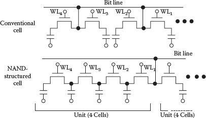
FIGURE 3.3
Comparison of the NAND-structured cell with a conventional cell. (Redrawn from “An Experimental DRAM with a NAND-Structured Cell,” T. Hasegawa et al., IEEE. J. Solid State Circuits, Vol. 28, pp. 1099–1104, 1993.)
Up to 16 Mbit DRAM generation conventional LOCOS isolation was used but beyond that bird’s beak scaling faced serious problems. For the cell pitch less than 0.4 μm modified LOCOS isolation techniques were employed [40]. Polysilicon spacered LOCOS (PSL) is a simple isolation scheme based on conventional LOCOS, in which drawn isolation size of 0.2 μm could be achieved [41]. PSL isolation had low bird’s beak encroachment and good vertical profile. Another isolation technology at 64–256 Mbit range is self-aligned LOCOS trench (SALOT) [42], which has the isolation structure of a poly-buffered LOCOS field oxide and a self-aligned trench at the center of a field region. However, for gigabit density DRAM, requirement of the scalability and the planarity could be achieved using shallow trench isolation (STI) with dual slope trench etching [43] followed by chemical mechanical polishing (CMP).
By 1998, 256 Mbit DRAMs were in mass production while 1 Gbit and even 4 Gbit experimental DRAMs were presented in conferences [43]. A highly manufacturable 1 Gbit SDRAM was fabricated, probably for the first time in 0.18 μm technology. The SDRAM used retrograded twin-well, shallow trench isolation; Ta2O5 based storage capacitor with HSG, a TiSi2 gate, W plug and W wiring process followed by relaxed double metallization and CMP process for global as well as local topography [44]. It is observed that most of the technologies employed were in line with the expected technology trends for DRAM process modules shown in Table 3.1 in a study by Nitayama and others [45]. These expected processes were thought to be based on the expected DRAM market needs of low cost, high speed, and so on, and preferably in embedded (logic) DRAM form. It was desired to use minimum chip area at the least possible temperature process and with metal word and bit lines.
Some Technology Trends for DRAM Process Module in a Gigabit Era
Module |
Concerns |
Possible Actions |
Lithography |
• Narrow process margin • KrF To ArF • Optical proximity effect • Thin resist process |
• Fully planarized process/mask critical dimension (CD) control • Optical proximity correction |
Capacitor (STC) |
• Step coverage/patterning • SN contact resistance, plasma damage |
• CVD BST/CVD Ru • BEOL process optimization |
STI |
• Trench fill • Stress reduction |
• HDP • High temp./thin oxidation |
Gate, S/D |
• Low resistance for gate • Low resistance for S/D |
• Poly/metal gate (ex. W/WN/Poly) • Co silicide |
Contact/MOL dielectric |
• Low temp. process • Void-less • Self-aligned contact |
• W dual damascene • HDP-PSG, TEOS-03 PSG, SAUSG • Selective etch to SiN cap |
Interlayer dielectric |
• Low k • Water absorption |
• FSG, k = 3.3–3.7 • Siloxane SOG, k = 2.6–2.8 |
Metallization |
• Low resistance interconnect • Patterning/gap fill |
• Cu wiring • Damascene |
3.5 Capacitor over Bit Line (COB) DRAM Cell
A simple idea of forming capacitor over bit line changed the memory cell structure and fabrication steps of the three-dimensional capacitor like the stacked capacitors and trench capacitors to a great extent. The COB technique enabled the memory cell to maintain sufficient storage capacitance with decreasing feature size. Up to around 4 Mbit DRAM density level, bit line was formed above the storage electrode. To get higher value of capacitance, storage electrode necessarily had to be taller in the three-dimensional case, as the capacitance was proportional to the total capacitor surface area including top/bottom and sidewalls. However, it made the formation of bit line contact and maximization of the storage electrode pattern difficult as shown in Figure 2.15 [46]. A unique structure for a COB cell was given by Kimura in 1988, wherein contact of the storage electrode to the active regions was formed through adjacent bit lines by a self-aligned process as shown in Figure 2.17 [17]. Inter-bit-line noise was almost eliminated because the bit lines were shielded by the storage electrode and holes needed in the plate for making bit line contact with the active region were no longer required.
A number of DRAM cells were realized based on COB technique. Some of these were mentioned in Section 2.8 and a few more shall be discussed now along with the issues involved in scaling down of COB stack DRAM cells.
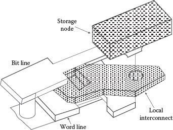
FIGURE 3.4
Perspective of the capacitor-over-bit-line (COB) cell with the hemispherical-grain (HSG) poly-Si storage node. (Redrawn from “A Capacitor-Over-bitline (COB) Cell with a Hemispherical-Grain Storage Node for 64 Mb DRAM,” M. Sakao et al., IEDM Tech. Dig., pp. 655–658, 1990.)
Feasibility of a COB cell for 64 Mbit DRAM was verified by Sakao and others in 1990 [47]. The given cell occupied chip area of 1.8 μm2 at 0.4 μm design rules, obtaining storage capacitance of 30 fF with storage node height of 0.5 μm. Use of hemispherical grains on the storage node allowed using reduced node height (to nearly half of that without hemispherical grain), for obtaining comparable value of storage capacitance. Perspective view for a COB cell with HSG poly-Si storage node is given in Figure 3.4. To make the COB cell structure, an additional local interconnect layer is laid for forming a connection between capacitor with the active area [47]. This additional layer formation allowed the use of a rectangular area against diagonal active area. Sakao and others gave another COB cell structure with straight-line-trench isolation and trench-gate transistor (SLIT) having potential for giga-bit DRAMs. As mentioned in Chapter 2, the SLIT cell overcame the limitation of complex active area pattern in the formation of capacitor contact in some previously reported COB structures [48]. Figure 3.5 shows a three-dimensional cross-section of the SLIT cell in which two types of trenches, the isolation trenches and the gate trenches, are formed orthogonally, defining the rectangular active area. Straight-lined isolation trenches isolate adjacent cells in one direction and the trench gate serving as field plate provides isolation in the orthogonal direction. Layout of the SLIT cell having a size of 6 F2 is shown in Figure 3.6(a). In this layout there is no alignment margin space, and it is produced using a simple pattern shrinking technique SAFE (side-wall aided fine pattern etching). Process sequence of SAFE technique is given in [48], which allows the trench to reduce to less than half of the design rule and layout of SLIT cell after the processing is shown in Figure 3.6(b). Storage node electrode is also made of poly-Si including scaled capacitor contact using the SAFE technique. An experimental cell array with 0.96 μm2 cell size was real-ized in 0.4 μm design rule.
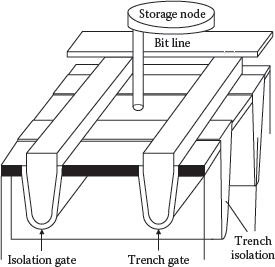
FIGURE 3.5
Simplified schematic view of the SLIT cell. (Redrawn from “A Straight-Line-Trench Isolation and Trench-Gate Transistor (SLIT) Cell for Giga-bit DRAMs,” M. Sakao et al., IEDM Tech. Dig., pp. 19–20, 1992.)
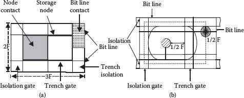
FIGURE 3.6
(a) Layout of the (2F*3F) SLIT cell; (b) plan view after processing. (Redrawn from “A Straight-Line-Trench Isolation and Trench-Gate Transistor (SLIT) Cell for Giga-bit DRAMs,” M. Sakao et al., IEDM Tech. Dig., pp. 19–20, 1992.)
A simple 4 Gbit DRAM is realized using high aspect-ratio pillar capacitor for COB type STC cell. The storage node and the peripheral vias are fabricated simultaneously with high aspect-ratio pillars, which allows using ON dielectric or Ta2O5; and surface is planar for metal wiring [49]. A pillar height of 1.5 μm provides a storage capacitance of 17 fF/cell for ONO film and 22 fF using Ta2O5. Self-aligning was also a key word in the fabrication as it was used for patterning of the cell plate, elevated source/drain by damascene and Ti salicidation of their surface, and formation of various metal contacts.
Realized Capacitance with Different Cylinder Heights [50]
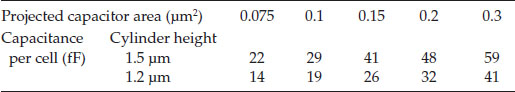
Maximization of poly-Si-based capacitor electrode surface area and hence cell capacitance was obtained through innovations in structures having fin, cylindrical, pillar shapes and HSG surface, use of higher dielectric constant materials like Ta2O5, and use of low temperature processing having low resistance, and fully metal-based technology. Most of these ideas were combined in a cylindrical full metal capacitor (FMC) electrode with integrated metal contact-hole plug for gigabit DRAMs [50]. In the proposed FMC technology-based cell conventional CVD-W/TiN/Ti was used for metal-based capacitor contact-hole plug and, for the multi-surface bottom electrode two different W cylinder formation processes were evaluated; an exterior process which employs an SiO2-core, PVD+CVD-W body and W-RIE, whereas the interior process employed an SiO2 frame, PVD+CVD-W body and W-CMP with a protective plug. Its results show that interior cylinder process is better for gigabit densities as it provides improved lithographic/RIE pattern stability, the PVD-W adhesion layer for CVD-W enables formation of a uniform W-only cylinder and W-CMP implementation results in superior cylinder shape. The single cell capacitance of the projected capacitor area W cylinder could go over 40 fF as per Table 3.2 [50], while using 1.6 nm SiO2 equivalent thick layer of Ta2O5 deposited with oxidation treatment such as O2 plasma.
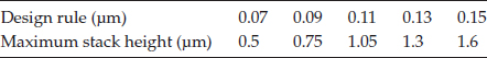
A COB memory cell with 0.1 μm design rule was fabricated using SRP (SAC spacer removal after plug implantation) a novel SAC process and DMO (dual molded oxide) capacitor process. The SRP process improves data retention time characteristics and minimizes short channel effect in cell transistor. Dual spacer and downstream surface cleaning process was used to cure the surface defects and minimize junction leakage current [51]. In the DMO process two oxide layers (BPSG+PE–TEOS) are deposited on etch stopping layer of Si3N4, then the two oxide layers are etched anisotropically. The bottom area of the storage node is enlarged during the precleaning process by about 20% due to different wet etching rates of the two oxide layers. Finally a 400 Å thick poly-Si was deposited to form one cylindrical storage node capacitor as shown in Figure 3.7. Mechanical stability of the COB stack cell becomes important for below sub-quarter micron technology and mechanical stability of the storage node decreases rapidly with scaling down. It results in putting a limit on the stack height of the memory cell capacitor according to the estimate given in Table 3.3; otherwise, storage node will be shortened [52]. It is this reason that the DMO process, which has better mechanical stability, is employed. The data retention characteristics of DMO capacitor are considerably better than that of a conventional one, and the improvement factor is at least three.
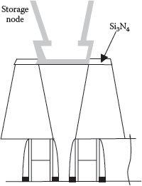
FIGURE 3.7
DMO OCS node capacitor. (Modified from “Highly Extendible Memory Cell Architecture for Reliable Data Retention Time for 0.10 μm Technology Node and beyond,” J. Lee et al., Proc. ESSDRC, pp. 571–574, 2002.)
Permissible Stack Height of Cylinder-Type COB Stack Cell at DRAM Technologies with Mechanical Stability
COB stack cells studied so far had some key features like planar structure of memory cell transistor with uniformly doped channel and three-dimensional structure of memory cell capacitor. In such a configuration independent design and optimization of memory cell transistor and storage node are not possible and needed new ideas to make it practical beyond 100-nm technology. Some other closely involved required technologies are advanced lithographic techniques and novel MIS/MIM capacitors. Another important consideration is to choose between open or folded bit line cell architecture. It has been observed that in spite of smaller capacitor and chip area (4F2/6F2) used in open bit line architecture, the folded bit line architecture was preferable on account of better noise immunity, though its cell used up 8 F2 of chip area. Additionally in the COB stack cell lower capacitor area was achievable. It was therefore, correctly assumed that a COB stack DRAM cell, combined with folded bit line architecture would be a good choice for further DRAM density advancements, while using below 100-nm technology, however with a rider that suitable solutions were available for foreseeable difficulties [53]. Issues connected with the process technologies like isolation dimension scaling, memory cell transistor parasitics, reduction in cell capacitance, and non-reduction of bit line capacitance with scaling down have been identified. If problems are attended to satisfactorily, scaling-down effects on degrading DRAM cells such as increased parasitic resistance and node junction leakage current, variation of threshold voltage, and so on, could be overcome.
A common practice for cell-to-cell isolation is the implantation of channel stop using either LOCOS or STI. But this practice degrades data retention line and the problem becomes severe in sub 100-nm technology node. In addition, serious cross talk occurs among memory cells and severe inverse narrow width effect, etc. takes place. To overcome such a host of problems, a metal shield embedded STI (MSE-STI) [54] for isolation technology beyond 100 nm node is suggested. The MSE-STI is able to eliminate the cell-to-cell cross talk and with a provision of negative bias to the embedded metal, channel stop implantation would be avoided, so the degradation of data retention time should be halted.
A number of new issues crop up when the dimensions of the cell transistor become very small. Constraints of the lithographic and other fabrication processes produce variation in physical dimensions and other features like doping profile, which results in large fluctuations in transistor parameter like threshold voltage [55]. The amount of the variation in the threshold voltage tends to be inversely proportional to the minimum feature size. It is important to control dimensional and other variations, so that variations in threshold voltage of the cell transistor are minimized. Cell transistor is also degraded due to short channel effect and narrow width effect at smaller dimensions. Another important issue for the cell transistor is leakage current of the storage node junction. Beyond the 100 nm technology node, the junction leakage current is primarily decided by perimeter-type junction leakage current [56]. The most effective way to reduce the junction leakage current is to lower the substrate doping density underneath storage node junctions. However, it is contradictory to the requirement of increasing the channel doping density for keeping threshold voltage of nearly 1 V. Moreover, current drive capability of the cell is also reduced with unscalable threshold voltage and reduced channel mobility if its doping is increased. One alternative to overcome this problem is to use local channel implantation technology for selective doping of the channel of the memory transistor leading to spike-doped channel technology; only a small portion of channel has high doping concentration and the other areas have low concentration. For example, in 70 nm memory cell transistor, the substrate doping density underneath storage node junction can be reduced from 1 × 1018 cm–3 with a conventional channel to 1 × 1017 cm–3 in spike channel [53]. The spike-domed channel has the added advantage of reducing the short channel effect and increased robustness in terms of fluctuations of transistor parameter due to variations in its dimensions, width, and length. Since the spike-doped region located at the center of the channel suppresses the electric field penetration from the drain to the source, it also reduces the drain-induced barrier lowering (DIBL) effect.
Another issue for sub-100 nm COB stack DRAM cell is that of realizing a minimum capacitance of 25 fF/cell, a problem common to other types of cells. Therefore the solutions are also on the same lines which are applicable in other cases, that is, use of thinner/different dielectric and use of innovative MIS or MIM capacitors. In addition, increase of stack height of cylinder-type COB stack cell sometimes results in mechanical stability problems, leading to inter-storage node shorting or twin bit failure. Thus the minimum height of the stack is limited as was mentioned in Table 3.3. Mechanical stability of the storage node becomes a serious issue. It will be discussed in Chapter 6, especially for more COB stack DRAM cells. A suggested combination for COB stack capacitor technology for DRAM technology is given in Table III of ref. [53]. It is observed that though HSG continued to be used, the storage node of box-shape was replaced by a cylinder-shaped one at 0.13 μm technology which itself was replaced by merged structure of cylinder-box shape. Changeover from MIS capacitor to MIM was nearly complete around 100 nm stage but equivalent oxide thickness remained nearly constant up to 0.11 μm (37 Å to 30 Å) which decreased considerably later to 15 Å at 90 nm and ~5 Å at 70 nm, respectively, with the use of much higher dielectric constant material and metal electrodes.
One of the challenging issues for future technology is to keep parasitic bit line capacitance to a low value as well as maintaining a low resistance. It is observed that up to around 0.15 μm technology bit line parasitic capacitance follows set rules for its evaluation, but beyond that it tends not to be reduced in spite of dimension scaling and remains nonscalable beyond 100 nm. This nonscalable nature of bit line capacitance is due to increased inter-bit line capacitance and capacitance between bit lines and other conducting layers. This problem of nonscalable bit line capacitance can be overcome with a hierarchical bit line scheme, a combination of global and segmented bit lines. The global bit lines do not have parasitic capacitance between bit line and other conducting lines like word lines. Since the total parasitic capacitance is the sum of global bit line and segmented bit line capacitance, overall capacitance gets reduced. DRAM technologies employed by 2002 were discussed here briefly. Few representative reports were discussed without detailed descriptions. It is expected that readers will get a fair idea of the sequence of technology developments. Advanced DRAM technologies will be discussed in Chapter 6. But before that, the advancements in the storage capacitor formation and the access transistor structures are addressed in Chapters 5 and 4, respectively, for better understanding of the technologies discussed in Chapter 6.
1. C. Mazure et al., “Technology Challenges and Solution for 1 Gbit and Beyond,” Integrated Ferroelectronics, Vol. 21, pp. 15–25, 1998.
2. W.M. Regitz and J. Karp, “A 3-Transistor Cell 1024 bit 500ns MOS RAM,” Dig. of Tech. Papers, ISSCC, 1970.
3. L. Boonstra et al., “A 4096-b One Transistor per Bit Random Access Memory with Internal Timing and Low Dissipation,” IEEE J.Solid State Circuits, Vol. SC-8, p. 305, 1973.
4. R.H. Dennard, “Field-Effect Transistor Memory,” U.S. Patent 3,387,286, June, 1968.
5. K.U. Stein et al., “Storage Array and Sense/Refresh Circuit for Single-Transistor Memory Cells,” Dig. Tech. Papers, ISSCC, pp. 56–57, 1972.
6. R. Proebsting and R. Green, “A TTL Compatible 4096-Bit n-Channel RAM,” Dig. Tech. Papers, ISSCC, pp. 28–29, 1973.
7. R.R. Schroeder and R.J. Proebsting, “A 16k × 1 Bit Dynamic RAM,” Dig. Tech. Papers, pp. 12–13, 1977.
8. L.G. Heller and D.D. Spampinato, “Cross-Coupled Charge-Transfer Sense Amplifier,” U.S. Patent 4,039,861, Aug. 1977, also L. Heller, “Cross-Coupled Charge Transfer Sense Amplifier,” IEEE ISSCC Tech. Dig., p. 20, 1979.
9. H. Miyamato et al., “A Fast 256k × 4 CMOS DRAM with a Distributed Sense and Unique Restore Circuit,” IEEE J.Solid-State Circuits, Vol. SC-22, 1987.
10. P. Gillingham et al., “High-Reliability Circuit Design for Megabit DRAM,” IEEE JSS Circuits, Vol. 26, no. 8, pp. 1171–1175, 1991.
11. N.C. Lu and H.H. Chao, “Half-VDD Bit-Line Sensing Scheme in CMOS DRAMs,” IEEE J.Solid State Circuits, Vol. SC-19, p. 451, 1984.
12. H. Sunami et al., “A Corrugated Capacitor Cell (CCC) for Megabit Dynamic Memories,” Proc. IEDM, pp. 806–808, 1982.
13. W. Wakamiya et al., “Novel Stacked Capacitor Cell for 64 Mb DRAM,” Symp. VLSI Technol. Dig. Tech. Papers, pp. 31–32, 1989.
14. K. Koyama et al., “A Stacked Capacitor with (BaxSr1-x) TiO3 for 256 M DRAM,” IEDM Tech. Dig., pp. 823–826, 1991.
15. M. Aoki et al., “A 60 ns 16-Mbit CMOS DRAM with a Transposed Data Line,” IEEE J.Solid State Circuits, Vol. 23, pp. 1113–1111, 1988.
16. H. Arima et al., “A Novel Stacked Capacitor Cell with Dual Cell Plate for 64 Mb DRAMs,” IEDM, pp. 651–654, 1990.
17. S. Kimura et.al, “A New Stacked Capacitor DRAM Cell Characterized by a Storage Capacitor on a Bitline Structure,” IEDM, pp. 596–599, 1988.
18. T. Takashima, “Word-Line Architecture for Constant Reliability 64 Mb DRAM,” Proc. Symp. VLSI Circuits, p. 57, 1991.
19. T. Kaga et al., “Crown-Shaped Stacked-Capacitor Cell for 1.5 V Operation 64-Mb DRAMs,” IEEE Electr. Dev., Vol. 38, pp. 255–260, 1991.
20. T. Kure et al., “VLSI Device Fabrication Using a Unique, Highly-Selective Si3N4 Dry Etching,” IEDM Tech. Dig., pp. 757–759, 1983.
21. H. Shichijo, “DRAM Technology Trend and Prospect,” Proc. VLSI-TSA, pp. 349–353, 1991.
22. T. Kaga et al., “A.29 μm2 MIM-CROWN Cell and Process Technologies for 1 Gigabit DRAMs,” IEDM Tech. Dig., pp. 927–929, 1994.
23. T. Kaga et al., “Advanced OSELO Isolation with Shallow for High-Submicrometer ULSIs,” Trans. IEEE Electr. Dev., Vol. 35, pp. 893–898, 1988.
24. K. Sagara et al., “A o.72 μm2 Recessed STC (RSTC) Technology for 256 Mbit DRAM Using Quarter-Micron Phase-Shift Lithography,” Symp. VLSI Techn. Dig., pp. 10–11, 1992.
25. Y. Nakagome et al., “An Experimental 1.5 V 64-Mb DRAM,” IEEE J.Solid State Circuits, Vol. 26, pp. 465–472, 1991.
26. H. Hidaka et al., “A Divided/Shared Bit-Line Sensing for VLSI DRAMs,” IEEE J.Solid State Circuits, Vol. 26, pp. 473–478, 1991.
27. K-Shibahara et al., “1 GDRAM Cell with Diagonal Bit-Line (DBL) Configuration and Edge Operation MOS (EOS) FET,” IEDM Tech. Dig., pp. 639–642, 1994.
28. M. Saito, T. Mori, and H. Tamura, “Electrical properties of thin Ta2O5 films grown by chemical vapour deposition,” IEDM Tech. Dig., pp. 680–683, 1986.
29. Y. Numasawa et al., “Ta2O5 Plasma CVD Technology for DRAM Stacked Capacitors,” IEDM Tech. Dig., pp. 43–46, 1989.
30. H. Shrinki and M. Nakata, “UV-O3 and Dry O3: Two-Step-Annealed Chemical Vapour Deposited Ta2O5 Films for Storage Dielectrics of 64 Mb DRAM,” IEEE Trans. Electr. Dev., Vol. 38, pp. 455–462, 1991.
31. S. Kamiyama and T. Saeki, “Highly Reliable 25 nm Ta2O5 Capacitor Process Technology for 256 Mbit DRAM,” IEDM Tech. Dig., pp. 827–830, 1991.
32. H.K. Kang et al., “Highly Manufacturable Process Technology for Reliable 256 Mbit and 1 Gbit DRAMs,” IEDM Tech. Dig., pp. 635–638, 1994.
33. Y. Takaishi, M. Sakao, and S. Kamiyama, “Low-Temperature Integrated Process below 500°C for Thin Ta2O5 Capacitor for Giga-Bit DRAMs,” IEDM Tech. Dig., pp. 839–842, 1994.
34. K.W. Kwon et al., “Ta2O5 Capacitors for 1 Gbit DRAM and Beyond,” IEDM Tech. Dig., pp. 835–838, 1994.
35. P-Y. Lesaicherre et al., “A Gbit-Scale DRAM Stacked Capacitor Technology with ECR MOCVD SrTiO3 and RIE Patterned RuO2/TiN Storage Nodes,” IEDM Tech. Dig., pp. 831–834, 1994.
36. C.V. Teng, “DRAM Technology Trend,” Proc. VLSI Techn. Systems and Appl., pp. 295–299, 1995.
37. T. Sugibayashi et al., “A 30-ns Mb DRAM with a Multidivided Array Structure,” IEEE J.Solid State Circuit, Vol. 28, pp. 1092–1098, 1993.
38. T. Hasegawa et al., “An Experimental DRAM with a NAND-Structured Cell,” IEEE J.Solid State Circuits, Vol. 28, pp. 1099–1104, 1993.
39. G. Kitsukawa et al., “256-Mb DRAM Circuit Technologies for File Applications,” IEEE J.Solid State Circuits, Vol. 28, pp. 1105–1113, 1993.
40. C.G. Hwang, S.I. Lee, and M.Y. Lee, “The State of the Art and Future Trends in DRAMs,” Proc. ESSDRC, pp. 37–44, 1995.
41. D.H. Ahn et al., “A Highly Practical Modified LOCOS Isolation Technology for the 256 Mbit DRAM,” IEDM Tech. Dig., pp. 679–682, 1994.
42. T. Park et al., “Self-Aligned LOCOS/Trench (SALOT) Combination Isolation Technology Planarized by Chemical Mechanical Polishing,” IEDM Tech. Dig., pp. 675–678, 1994.
43. K.P. Lee et al., “A Process Technology for 1 Giga-Bit DRAM,” IEDM Tech. Dig., pp. 907–910, 1995.
44. T. Murutami et al., “A 4-Level Storage 4 Gb DRAM,” ISSCC Tech. Dig., pp. 74–75, 1997.
45. A. Nitayama, “Future Directions for DRAM Memory Cell Technology,” IEDM Tech. Dig., pp. 355–358, 1998.
46. M. Koyanagi et al., “Novel High Density, Stacked Capacitor MOS RAM,” IEDM, pp. 348–351, 1978.
47. M. Sakao et al., “A Capacitor-Over-Bitline (COB) Cell with a Hemispherical-Grain Storage Node for 64 Mb DRAM,” IEDM Tech. Dig., pp. 655–658, 1990.
48. M. Sakao et al., “A Straight-Line-Trench Isolation and Trench-Gate Transistor (SLIT) Cell for Giga-bit DRAMs,” IEDM Tech. Dig., pp. 19–20, 1993.
49. S. Nakamura et al., “A Simple 4 G-bit DRAM Technology Utilizing High-Aspect-Ratio Pillars for Cell-Capacitors and Peripheral-Vias Simultaneously Fabricated,” IEDM Tech. Dig., pp. 29–32, 1997.
50. J.M. Drynan et al., “Cylindrical Full Metal Capacitor Technology for High Speed Gigabit DRAMs,” Symp. VLSI Techn. Dig. Tech. Papers, pp. 151–152, 1997.
51. J. Lee et al., “Highly Extendible Memory Cell Architecture for Reliable Data Retention Time for 0.10 μm Technology Node and Beyond,” Proc. ESSDRC, pp. 571–574, 2002.
52. Y. Park and K. Kim, “COB Stack DRAM Cell Technology beyond 100 nm Technology Node,” IEDM Tech. Dig., pp. 391–394, 2001.
53. K-Kim and M-Y. Jeong, “The COB Stack DRAM Cell at Technology Node below 100 nm-Scaling Issues and Directives,” IEEE Trans. Semiconductor Manufacturing, Vol. 15, pp. 137–143, 2002.
54. J.H. Sim, J.K. Lee, and K. Kim, “High-Performance Cell Transistor Design Using Metallic Shield Embedded Trench Isolation (MES-STI) for Gigabit Generation DRAM’s,” IEEE Trans. Electr. Dev., Vol. 46, pp. 1212–1217, 1999.
55. T. Mizuno et al., “Performance Fluctuations of 0.1 μm MOSFETs—Limitations of 0.1 μm ULSI’s,” Proc. Symp. VLSI Techn. Dig. of Tech. Papers, pp. 13–14, 1994.
56. J.Y. Lee, D.W. Ha, and K. Kim, “Novel Cell Transistor Using Retracted Si3N4-Linear STI for the Improvement of Data Retention Time in Gigabit Density DRAM and Beyond,” IEEE Trans. Electr. Dev., Vol. 48, pp. 1152–1158, 2001.