Storage Capacitor Enhancement Techniques
One of the most critical issues in DRAM cell designs is the fabrication of sufficient value reliable storage capacitance while cell size is continuously decreasing. In the beginning, SiO2 was the dielectric used in planar forms of capacitors and reduction in its thickness was the main option for maintaining realized capacitance value with increasing DRAM density. However, beyond 4 Mbit, high leakage prevented further reduction in dielectric thickness and alternatives in the form of the use of materials other than (only) SiO2, structural innovations in the cell, and modification in electrode surface were applied.
In the discussion of the development of DRAMs from 16 Mbit onwards to around 1 Gbit in Section 3.4 of Chapter 3, problems associated with the necessity of fabrication of storage capacitor in ever-decreasing chip area were clearly emphasized. In that period of DRAM development SiO2 and its combination with silicon nitride was replaced with higher dielectric constant Ta2O5. In addition, the capacitor was realized in three dimensions instead of being planar; the crown-shaped capacitor was a preferred shape. At 256 Mbit and 1 Gbit level, high dielectric constant material like BST film was also used. Storage nodes other than polysilicon, like RuO2/TiN, were employed. In addition, texturing of the bottom plate of the capacitor through formation of hemispherical grain (HSG) was used to increase the effective capacitor area (hence its value). In Section 5.2 generation of HSG on the storage node shall be discussed along with the variations in the properties of HSGs on account of process and processing temperature used. Properties of higher permittivity and layered dielectric involving SiO2 and Si3N4, using slightly varying fabrication processes is then taken up. It is followed up with description of capacitors formed using Ta2O5 as dielectric, whose properties get changed with the method of deposition of Ta2O5, annealing temperature and metal used for the electrodes. Since in embedded DRAMs processing temperature should be lower, formation of HSG in such cases is also discussed briefly in Section 5.4.
A different kind of technology is used for storage capacitance fabrication in trench DRAMs for sub-100 nm design rules. Bottle-shaped trenches with Al2O3 film for an aspect ratio more than 60 have been realized. Application of growth of HSG in such capacitors is given in Section 5.5. Metal-insulator-metal (MIM) capacitor structures using materials with increasing value of dielectric strength material like Ta2O5, BST, HfO2, ZrO2, and layered combinations of some of these materials are taken up next. Use of different metals for the top and bottom electrodes while using mentioned dielectrics has also been described. A common theme is that it is always important to monitor the reliability of the fabrication capacitor especially in terms of its leakage current density and the compatibility of the all the materials used so that their combinations do not degrade the quality of the capacitor and the DRAM cell.
5.2 Hemispherical Grain Storage Node
Before depositing thin dielectric layer, texturing of the bottom polysilicon electrode of poly-to-poly capacitor was initially realized by Fazan and Lee [1] to increase its capacitance without increasing its projected area. The effective storage surface area was increased by more than 30% due to the creation of asperities on the polysilicon surface and the technique was later found to be applicable in all stacked or trench capacitor cells which had a bottom polysilicon electrode. Increase in capacitor area due to the creation of the texture depended strongly on the polysilicon deposition temperature, polysilicon thickness, doping process, and oxidation temperature [2]. For measuring electrical characteristics in such schemes, after texturing, polysilicon, a highly reliable composite oxide/nitride dielectric was formed by depositing a 10 nm thick Si3N4 using LPCVD and slight reoxidation [3]. Top capacitor plate of ~200 nm thick polysilicon was then deposited to form the capacitor. Maximum capacitance increased to 6.7 from 5 fF/μm2 with the textured bottom plate. Leakage current was measured through the textured structure and slight increase was observed at high fields; however, at low or operating fields no difference was observed. This increase in leakage can be understood by following the difference between electrical conduction mechanism through SiO2 and Si3N4. In SiO2 conduction is through Fowler-Nordheim emission and leakage current depends on the electric field near the injecting electrode and increases considerably due to the presence of asperities. In Si3N4 conduction is bulk-limited and governed by Frenkel-Pool emission which is due to field-enhanced thermal excitation of trapped electrons [4]. Other important electrical characteristics such as the time-dependent dielectric breakdown (TDDB) measurement at the operating field of 3.6 MV/cm showed that textured capacitors have much higher lifetime values than the non-textured or smooth capacitors [1].
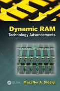
A hemispherical grain (HSG) poly-Si storage node has been developed at 64 Mbit DRAM density level for a capacitor-over-bit-line (COB) cell structure [5]. Figure 3.4 showed a perspective view for the cell with HSG poly-Si storage node, which doubled the effective surface area in comparison to that of conventional smooth poly-Si and hence helped in eliminating the need of using a complex storage node structure and reduced storage node height. The HSG storage node fabrication requires two additional process steps, that is, HSG poly-Si deposition and an etch back as shown in Figure 5.1. After the formation of capacitor contact and conventional storage node, HSG poly-Si is deposited on core storage node. The HSG poly-Si is etched back by reactive ion etching with HBr gas. For a 1.8 μm2 memory cell at 0.4 μm minimum feature size, a 0.5 μm high poly-Si storage node with 0.1 μm spacing covered with hemispherical grain was formed after the etch back, which provided storage capacitance of 30 fF, an increase of more than 100% in value without surface texturing.
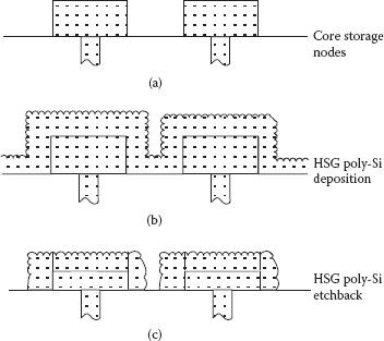
FIGURE 5.1
Fabrication steps for HSG poly-Si storage nodes for enlargement of storage node area by the HSG poly-Si deposition and etch back. (“A Capacitor-over-Bitline (COB) Cell with a Hemispherical Grain Storage Node for 64 Mb DRAMs”, M. Sakao, et al., IEDM, pp. 655–658, 1990.)
Since the dielectric films with less than 3 nm SiO2 equivalent thickness are required, stacked capacitor cells using oxide-nitride-oxide (ONO) layers can hardly satisfy the requirements of cell area and storage capacitance beyond 64 Mbit DRAM level. To overcome this problem engraved storage electrode poly-Si film (Figure 5.1), which has a rugged surface, was used [6, 7 and 8]. However, it was observed that the surface morphology of poly-Si film deposited by LPCVD changes with the deposition temperature [9]. It was also observed that poly-Si film deposited at 560°C has both amorphous area and polycrystalline area with hemispherical shape grains. The grain diameter increased and grain density also decreased with rise in working temperature and at 565°C grain shape changed from hemispheric to cylindrical and amorphous area disappeared. At still higher temperature of 580°C small grains combine together and form smooth polycrystalline film [10]. Poly-Si storage elctrode deposited at about 570°C has rugged surface and Si3N4 film deposited at 620°C. A 0.1 μm poly-Si film achieved 2.5 times more surface area than the storage electrode deposited at 620°C, which made it suitable for 64 Mbit DRAM and beyond. It is necessary to improve oxidation resistance of thin Si3N4 film if it is to be used as ONO composite film. It is observed that deposition temperature considerably affects the oxidation resistance of the Si3N4 film; when deposited at 600°C it has higher oxidation resistance than the film deposited at conventional temperature of 900°C.
Ultra-thin oxide/nitride dielectric layer is needed for 64 and 256 Mbit stacked DRAMs, but when the thickness of the nitride film is reduced to less than 4 nm range, an abrupt drop in capacitance appears. This sharp transition occurs when the ultra-thin nitride film is unable to withstand the following reoxidation step [11], which grows a thick film on the heavily doped bottom polysilicon electrode. Because of the possibility of the oxidation punch-through mechanism it imposes an upper limit to the maximum capacitance of 6.9 and 12.3 fF/μm2 for smooth and rugged structures, respectively, which can be realized with ON dielectric. The capacitance increase of 80% using ON films on rugged polysilicon was as high as the maximum values reported for Ta2O5 high dielectric constant-material used with smooth surface in the years 1990–91 [12].
A different surface modifying method was developed by Jun and others in 1992 to obtain a modulated stacked (MOST) capacitor, in which surface area of the storage electrode was increased up to eight times that of an ordinary stacked capacitor [13]. Usual process steps are taken to form structure below the stacked capacitor and to form its first electrode; an amorphous silicon layer is deposited. An oxide layer of approximately 100 nm is deposited and then top poly-Si layer is deposited under controlled pressure and temperature conditions. This layer has rough surface consisting of hills and valleys. Subsequent processing steps leave the storage electrode poly-Si in pillar form. Then a composite ON layer of dielectric is formed and finally a 200 nm thick poly-Si layer to form capacitor plate electrode. Electrical properties such as leakage current, breakdown voltage, and TDDB are comparable to those of conventional stacked capacitors.
The conventional oxide/nitride (ON) dielectric used in 4 Mbit and 16 Mbit DRAMs can provide capacitance values on the order of 6–7 fF/μm2 for 3.3 V supply [14]. For 64 and 256 Mbit stacked memory chips high dielectric constant Ta2O5 films on rugged poly-Si bottom electrode have been suggested which are able to provide capacitance values as high as 12 fF/μm2 [5,12,14]. However, a chemical vapor deposited (CVD) thin Ta2O5 film with rugged poly-Si and a high capacitance of 20.4 fF/μm2 without increasing projected area can be achieved, without degrading the leakage current, and TDDB characteristics, as shown in a simple stacked cell of Figure 5.2 [15]. A 150 mm <100> silicon wafer is covered with a 200 nm thick SiO2 layer and 100 nm thick poly-Si is deposited at 550°C to form rugged hemispherical grained bottom electrode structure. A 15 nm thick Ta2O5 film is then deposited at 400 or 450°C, which is annealed by rapid thermal annealing (RTA) process to reduce leakage current. Finally the top electrode is deposited. It is observed that when compared to standard ON/smooth structures, Ta2O5/rugged poly-Si capacitor fabrication in core or crown-shaped capacitor for 0.5 μm2 256 Mbit DRAM cell, the node height is reduced by a factor of three or more, which considerably reduces topography issues. Excellent leakage current, TDDB characteristics, and capacitor values of more than 20 fF/μm2 make the given structure very suitable for 256 Mbit DRAM applications. Another cylindrical capacitor structure using hemispherical grained-Si developed for 256 Mbit DRAM by Watanabe and others [16] achieves a cell capacitance of 30 fF with 0.4 μm high storage electrodes in a 0.72 μm2 cell area. The HSG-Si cylindrical capacitor was developed by applying the seeding method [17] in which Si molecular beam deposition and subsequent annealing are done to form Si microcrystals on undoped amorphous Si surface, along with the use of a vapor hydrogen fluoride (HF) selective etching. Under the low-pressure vapor HF etching, high selective etching of borophosphosilicate glass (BPSG) to SiO2 is obtained. The cylindrical electrode is simply formed by this selective etching method. Figure 5.3 shows the process flow of a HSG-Si cylindrical capacitor. Grain size was controlled through adjusting annealing time. Both sides of the electrode walls could be covered with HSGs.
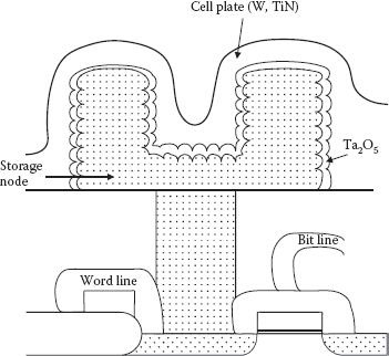
FIGURE 5.2
Cross-sectional view of a typical capacitor structure combining HSG and Ta2O5 for 256 Mb DRAMs. (Redrawn from “A High-C capacitor (20.4 fF/µm2) with ultrathin CVD Ta2O5 Films Deposited on Rugged Poly-Si for High Density DRAMs”, P.C. Fazan, et al., IEDM, pp. 263–266, 1992.)
FIGURE 5.3
Process flow of an HSG-Si cylindrical capacitor. (“A New Cylindrical Capacitor Using Hemispherical Grained Si (HSG-Si) for 256 Mb DRAMs”, H. Watanabe et al., IEDM, pp. 259–262, 1992.)
BPSG film was used as the core to form cylinders. BPSG and p-doped amorphous-silicon films for the bottom electrode was patterned by lithography and reactive ion etching. A cylindrical wall electrode was formed by deposition and successive etch back of the p-doped amorphous silicon film. The core BPSG was selectively removed by using LP HF vapor etching. Native oxide on the cylindrical electrode was removed and HSG-Si appeared on p-doped amorphous Si surface using the seeding method, Si2H6 molecule irradiation, and annealing at 580°C in ultra-high vacuum chamber. A 5.0 nm SiO2 equivalent-thick SiO2/Si3N4 film was formed on the HSG-Si cylindrical electrode.
The influence of the temperature during Si2H6 molecule irradiation and subsequent annealing was investigated both for undoped and p-doped amorphous Si [18]. It is observed that small and large HSG-Si grains cover the whole surface of an electrode formed on an undoped amorphous Si at 600°C and that HSG-Si partially covers the surface of the electrode formed on a p-doped amorphous Si film at the same temperature, whereas uniform size HSG-Si covers the electrode surface formed on p-doped amorphous Si at 580°C. It was also observed that grain-size of HSG-Si increased and the thickness of cylindrical wall decreased with increasing annealing time. Realized capacitance increased 1.6 times after 10 second annealing, 2.0 times after 30 seconds and 2.3 times after 55 seconds; however, if annealing is continued even after that the grains become almost spherical and the cylindrical wall disappears [18]. Similar attempt was made to obtain rugged poly-Si cell structure at 256 Mbit DRAMs density level having low aspect storage node without any complex process [19]. In this scheme double-sided rugged poly-Si fin STC technology is used in which the shape of the rugged poly-Si is controlled by ion implantation. The separated-grain poly-Si is deposited by LPCVD. The shapes of the grains are changed by ion implantation with arsenic dose more than 5E15 per cm2 and neighboring grains get connected to each other. Cell capacitance reaches 25 fF/cell in STC with 2 fins having 4.5 nm thick ONO film and the storage node height is reducible to 300 nm.
Above examples show the formation of HSG-Si using different forms of capacitor structures like fin, stacked, cylindrical, or trench type, with different dielectrics like ON, ONO, Ta2O5. Methods of formation of grains like seeding/annealing or ion implantation and variation in temperatures were used and slightly varying results were obtained. Investigation was made by A. Ils and others [20] on the formation of HSG-Si on undoped and doped amorphous silicon by the seed and anneal techniques; effects of dopants on grain formation were also studied. For undoped amorphous Si, it was not only confirmed that Si atoms near the seed migrated more toward the seed to form HSG and the depression around [21], but the original silicon surface moves progressively toward the substrate with longer annealing due to nucleation. It was assured that in this case HSG-Si is formed through nucleation and by mass transport, which results in mushroom-shaped grain. For the p-doped amorphous Si case no depletion was found around the grains and the annealing time had little effect on grain size, which was much smaller. It was concluded that grains were formed mainly from the epitaxial growth, which takes place during seeding.
While forming grained polycrystalline Si film for DRAM storage capacitor, it is important to determine its electrical properties. Study shows that a strong correlation exists between the surface roughness measured in terms of reflectance and the electrical area enhancement factor (AEF) of the film. Leakage current density of the device with rough electrode is less than the AEF times that of the device with controlled poly-Si electrode. It is shown that the morphology roughness and doping of the film strongly affect the electrical performance of the capacitor [22].
5.3 Higher Permittivity and Layered Dielectrics
For 1 Gbit DRAM, the cell area is typically 0.24 μm2. To realize 30 fF in this small area high permittivity materials like BaSr, TiO3, Pb, and lead, zirconium, and titanium oxides are recommended. However, ultra-thin Ta2O5 capacitors can also give desirable results with low cost of ownership, though they require some key technologies, which are as follows [23]:
1. Use of tungsten for the storage node surface suppresses native oxide growth on the electrode, resulting in 40% reduction of the SiO2 equivalent thickness in comparison with n+ poly-Si electrode [24].
2. New oxygen plasma annealing for Ta2O5 film reduces leakage current.
3. The tungsten film is to be prepared by LPCVD on the HSG-Si structure.
By adapting the aforementioned technologies, the storage capacitance increased 2.6 times over that of a conventional stacked capacitor, reaching a value of 29.6 fF/μm2 (against 20.4 fF/μm2 for Ta2O5/HSG-Si capacitor structure). This cell capacitance is obtained with 0.6 μm-high HSG-Si storage-node in a 0.24 μm2 cell area. Leakage current characteristic is almost the same as that of no-HSG structure. It indicates that the 1.6 nm equivalent thick Ta2O5 capacitor on HSG structure with 10–8 A/cm2 at half of 1.5 V operating voltage can be achieved.
Even with the use of high dielectric constant films, a simpler planar stacked capacitor cannot provide a cell capacitance with such a small area available for it beyond 1 Gbit DRAMs. Hence a three-dimensional capacitor is developed in which sputtered TiN of the TiN/poly-Si electrode is replaced with the plasma enhanced CVD-WN [25].
Before the development of 256 kb DRAMs, only SiO2 was used as the dielectric, however, with the development of 256 Kbit DRAM oxide-nitride-oxide/oxide-nitride (ONO/ON), multilayered dielectric has been used [5,10,12,16], which resulted in higher effective dielectric constant and lower defect density. Further, when DRAMs moved over to 1 Gbit range, complex cell structure using ONO/ON dielectric became no longer feasible and dielectrics with higher dielectric constant were required as their use simplified the cell structure and simple structure was translated to simpler processes, leading to low cost of production. Use of HSG-poly-Si while using different dielectrics and different structures was also very attractive.
Use of three-dimensional structures in Mbit DRAMs, SiO2 (es = 3.9), faced a reliability problem since locally reduced oxidation rates caused defects and reduced breakdown fields; hence, Si3N4 (er = 7.2) became the most practical dielectric when combined with rugged poly-Si electrode such as HSG poly-Si and/or three-dimensional capacitor structure. The development of ONO/ON capacitor film structure is shown in Figure 5.4 [26].
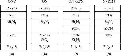
FIGURE 5.4
Film structure formation trends in Si3N4 capacitors. (“Trends in DRAM Dielectrics”, K.S. Tang, et al., Circuit and Devices, pp. 27–34, 1997.)
The ONO film structure of Figure 5.4(a) begins with thermal oxidation of bottom poly-Si, LP CVD deposition of Si3N4 and thermal oxidation of the Si3N4 film. Once the bottom oxide layer was removed for reducing the SiO2 equivalent thickness (toxeq) as shown in Figure 5.4(b), it is called ON. When toxeq becomes less than 5 nm, leakage current is dominated by direct tunneling, thus putting a limit to toxeq to 5 nm. A transition layer is formed when an initial layer of Si3N4 is deposited on the native oxide. As the Si3N4 film thickness is reduced, the tunneling leakage current rapidly increases. To overcome this problem, the native oxide was changed to a nitride layer through rapid thermal nitridation (RTN) on the polysilicon electrode surface before CVD of Si3N4 [26], as shown in Figure 5.4(c). For further improvement to N/RTN structure of Figure 5.4(d), processing steps are to be increased. However, there is general agreement that making use of ONO/NO for gigabit and beyond requires too many complex processes, hence higher dielectric constant materials are preferred [27].
Ta2O5 (er ~25) was found to be a very suitable dielectric for 256 Mbit and 1 Gbit DRAM capacitors as it could replace Si3N4 without major process integration problems. Many methods for depositing Ta2O5 film have been proposed, for example, CVD methods such as LP CVD, plasma-enhanced CVD (PECVD) and electron cyclotron resonance plasma-enhanced ECR PECVD. In the first half of 1980s Ta2O5 film formation using CVD method was widely adapted. The films were deposited on Si or metal-coated substrates by the thermal decomposition of tantalum ethylate. Film deposition was done between 450°C and 700°C, but high dielectric strength of nearly 26 was obtained at about 600°C. Dielectric constant of the Ta2O5 film was independent of its thickness for MIM structures, but reduces in value as the thickness decreases when film is grown on Si substrate [28].
High-temperature annealing is usually necessary to reduce the excessive leakage current of as-deposited Ta2O5 films probably due to the deficiency of oxygen in it. To reduce leakage current and to improve the electrical properties of CVD Ta2O5 capacitors, various post-deposition annealing techniques are proposed to fill vacancies with oxygen. Out of these, rapid thermal annealing (RTA) in N2O is found to be the most effective in suppressing leakage current. Another problem faced is that post-anneal Ta2O5 capacitors in DRAM cells have to withstand high-temperature processes such as borophosphosilicate glass (BPSG) reflow after capacitor formation and Ta2O5-based capacitors degrade seriously after BPSG reflow, which is caused by TiN oxidation at the TiN/BPSG interface [29]. However, high-temperature annealing is not needed in the PECVD and ECR-PECVD processes due to the crystallization of the Ta2O5 film and growth of interfacial SiO2 layer [27]. The PECVD processes are based on the utilization of a precursor activated through high-energy plasma, whereas the ECR-PECVD process creates plasma at low operating pressure using microwave as well as high magnetic field. The plate electrode in Ta2O5 film based capacitor is generally a stack of highly doped poly-Si/TiN or WN/Ta2O5/highly doped poly-Si. The stack of doped poly-Si/TiN or WN is used so that TiN or WN layer prevents the escaping of oxygen from the Ta2O5 film. Then doped poly-Si is used on top of the TiN or WN layer so that the metal electrodes are protected in subsequent process steps.
It is important to note that an interfacial oxide layer always grows during Ta2O5 film deposition and during any annealing process. Since this oxide has low dielectric constant, effective capacitance is reduced. Therefore, thickness of the interfacial oxide should be as small as possible. Bottom electrode material affects the interfacial oxide thickness. Use of platinum (Pt) bottom electrode completely eliminates the interfacial oxide layer, but it can be deposited only by physical vapor deposition. Other bottom electrode materials are TiN and W, which can be deposited by CVD. TiN was the most widely used material because of its stability, even at high temperatures. It may be noted that Ru bottom electrodes having Ta2O5 film were used only at the end of 1990s and shall be discussed at a later stage.
The downscaling limit of Ta2O5 capacitors is estimated to be around an equivalent oxide thickness of 1.5 nm [26]. Combined with poly-Si electrode and capacitance enhancement techniques such as HSG, Ta2O5 capacitors are practical up to 1 Gbit DRAMs; the effective capacitance is difficult to maintain/increase further. While successfully fabricating a 1 GB DRAM with Ta2O5 capacitor, slightly different reports were available about the possible thinning of Ta2O5 film. Accordingly the leakage current shall increase drastically if thickness of the film is less than 3.5 nm [25]. Of course, procedures have been used to reduce the leakage current but going below 3 nm was not advisable. Hence, to ensure a capacitance density of 145 fF/μm2 for a 1 Gbit DRAM, a three-dimensional capacitor was fabricated with 150 nm wide undercut having top electrode of TiN/poly-Si and WN/poly-Si as shown in Figure 5.5. It was observed that for a Ta2O5 capacitor, WN is comparable with TiN as electrode material in terms of leakage before BPSG flow; however after BPSG flow at 850°C for 30 minutes, leakage current in WN/poly-Si top electrode became one-order less (compared to the TiN/polySi electrode), which was less than 2 × 10–15 A/cell at 1.6 V.
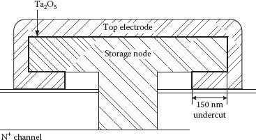
FIGURE 5.5
A stacked capacitor with 150 nm-wide undercut. (Redrawn from “Ta2O5 Capacitors for 1 G bit DRAM and Beyond”, K.W. Kwon et al., IEDM, pp. 835–838, 1994.)
Another 1 GB DRAM using a CROWN cell was given with CVD TiN top electrode and Ta2O5 film having SiO2-equivalent oxide thickness of nearly 1.6 nm. As three-dimensional bottom metal electrode could not be fabricated easily using conventional method of CVD or sputtering, a substituted tungsten (SW) electrode technology was developed in which W was substituted for poly-Si so that shape and thickness of the electrode could be processed easily [30]. Measured capacitance was nearly 17.1 fF/cell, but 20 fF/cell was reachable and the leakage current was nearly 0.1 μA/cm2 at a working voltage of 0.75 V. In spite of good electrical characteristics, a CVD-W-based storage node could not be used at 0.12 μm technology because of its surface morphology. Hence, a low-pressure CVD-WN technique was used for surface smoothing and an MIM cylinder storage node capacitor with an ultra-thin Ta2O5 was realized [31]. Improved technology and processes made it possible to realize 30 fF/cell capacitance in 0.25 × 0.5 μm2 and leakage was only 10–15 A/cell at 0.75 V.
In large-scale system integration, high-speed logic device processing and high-density embedded DRAM cell formation steps should be compatible and capacitor fabrication temperature should be lower than 700°C to suppress the degradation of CoSi2 in cobalt-salicided p+ diffusion layers. However, with lowering the process temperature, HSG grains are depleted which reduces the storage capacitance. A new low-temperature HSG cylinder ON capacitor process was developed by Yamamoto and others [32] as shown in Figure 5.6. Anisotropic silicon deposition is done and a cylindrical node is formed (Figure 5.6(a), (b)). After forming HSG grains on inner-type cylinders, ON dielectric film of 4–5 nm (equivalent SiO2 thickness) and top-plate-electrode were grown. For the development of low-temperature process, phosphorus doping to HSG grain with oxide-free surface by PH3 annealing was done at 700°C as shown in Figure 5.6(c) and TiN-plate electrode was used to suppress the depletion in the HSG grains and in the top electrode. Figure 5.6(c) shows the structure after top electrode formation. The process temperature was held below 700°C in the entire capacitor formation process. As an application, a graphic accelerator using 0.24 μm design rule embedded DRAM was fabricated at low temperature without degrading the performance of the logic devices.
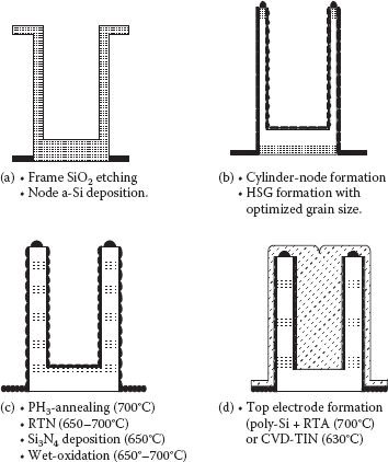
FIGURE 5.6
Low-temperature HSG cylinder ON capacitor process. (Redrawn from “Low-Temperature Metal/ON/HSG-Cylinder Capacitor Process for High Density Embedded DRAMs”, I. Yamamoto, et al., Symp. on VLSI Tech., pp. 157–158, 1999.)
To reduce the cost of ownership (COO) on account of using high-k dielectric a trench capacitor DRAM is realized [33] for embedded system using the trench DRAM as it appears to be more suitable for the logic LSI than the stacked DRAM [34]. To ensure enough capacitance, the scheme used gas phase doping (GPD) bottle-shape trench (BT) [35] and then HSG technique was applied for 0.08 μm trench capacitor. The BT technique increases the trench diameter and the HSG technique increases the sidewall area and realized capacitance is increased by nearly 5% with GPD, 10% with BT, and 50% with HSG, respectively. As the trench is deep, it is important to have uniform formation of HSG.
5.5 Sub-100 nm Trench Capacitor DRAMs
Important work has been done for capacitance enhancement in sub-100 nm trench DRAMs [36,37,38]. Use of bottle-shaped trench, integration of HSG, and replacement of ON dielectric by Al2O3 form a common theme with some variations in the process of the schemes. In fact, Al2O3 was used for the first time as high-k node dielectric in silicon-insulator-silicon (SIS) trench capacitor in 2001. However, deposition of Al2O3 film was done using atomic layer deposition (ALD) to achieve excellent step coverage at aspect ratios of up to ≈60, an essential requirement at 90 nm trench level [36].
Successful implementation of HSG on fully integrated trench wafer was achieved for the first time in 2001, and the thermal stability of Al2O3 in trench capacitor was also shown. Both selective and nonselective HSG processes have been developed for trench application. In the selective HSG process grains are formed selectively below the collar. Leakage versus tox data given in Table 5.1 for planar SIS Al2O3 capacitor (and oxide nitride capacitor) after annealing at 1050°C clearly demonstrates thermal integrity of Al2O3. A capacitance increase of up to 30% was achieved with leakage current remaining well below 1 × 10⁻⁸ A/Cm2 or 1 fA/cell. In a similar approach a manufacturable integration scheme for Al2O3 as node dielectric in trench capacitor was implemented in 170 nm technology, but claimed to be scalable below 100 nm [37]. Once a deep trench is formed, ALD process is used for Al2O3 film deposition and post-deposition annealing is done using rapid thermal process (RTP). First stage arsenic doped poly-Si deposition is done for the top electrode, then a recess is formed in it and Al2O3 is selectively removed as shown in Figure 5.7. At the final stage oxide collar is formed and the upper trench region is filled by a second poly-Si deposition. Obviously with decreasing minimum feature size and aspect ratio of trench being high (say >50), integration of thin Al2O3 film becomes demanding. Measured capacitance, in this report, was 36 fF/cell with 45 Å (angstrom) thick Al2O3 and leakage was 0.1 fA/cell at ± 1.0 V.
Variation of Leakage with tox for Planar Capacitor
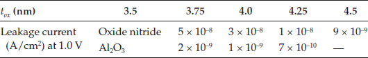
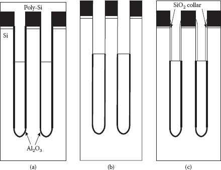
FIGURE 5.7
Schematic representation of the high-k integration flow. (a) After Al2O3 and poly-Si deposition, (b) poly-Si recess and selective Al2O3 removal, and (c) SiO2 collar formation and poly-Si fill. (Redrawn from “A Fully Integerated Al2O3 Trench Capacitor DRAM for Sub-100nm Technology”, H. Seidl, et al., IEDM, pp. 839–842, 2002.)
J. Lützen also used bottle-shaped trench capacitor with HSG deposition and Al2O3 dielectric for sub-100 nm DRAM. In trench technology for DRAMs, dielectric liner of sufficient thickness is required in the upper part of the trench to turn off the vertical parasitic device between the drain/buried strap region and the buried electrode of the capacitor. Conventional schemes reduce the trench diameter using oxide layer which increases the resistance of trench fill, thereby increasing RC delay, a constraint for future generations. A buried collar concept was implemented to increase enough space for the connection from the array device to inner electrode, as shown in Figure 5.8. Not only does the method result in lower node resistance, it does not require any sacrificial fills (resist or poly-Si) to define the depth of different features [38]. In the proposed scheme the integration of nonselective or selective HSG is straightforward [36,37]. Widening of the trench by wet etches and use of HSG deposition gives capacitance enhancement factor (CEF) of up to two. Proposed technology is compatible with high-k dielectric materials to be used with trench technology, which guaranteed values of more than 30 fF/cell at sub-100 nm ground rules. IBM Microelectronics fabricated a 512 Mbit prototype DRAM with a 84.6 mm2 die size using ArF lithography, utilizing an 8F2 vertical bottle-shaped, 6.5 nm deep trench, and hemispherical grains [39]. The technology was shown to be scalable without changing the basic architecture or cell layout.
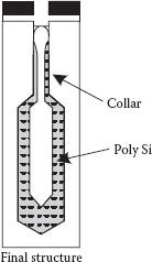
FIGURE 5.8
Buried collar concept. (Adapted from “Integration of Capacitor for Sub-100-nm DRAM Trench Technology”, Jorn Lützen et al., Symposium on VLSI Tech. Dig. Technical Papers, pp. 178–179, 2002.)
5.6 Metal Insulator Metal Structure
In Section 5.3 while progressing through the use of dielectric from SiO2 to its combination with silicon nitride and then application of Ta2O5, structure of the capacitor also changed from SIS (silicon-insulator-silicon) to MIS (metal-insulator-silicon) and then to MIM (metal-insulator-metal). The main aim was to realize increasing capacitance density while keeping leakage under control. Different metals were being used for the capacitor electrodes like TiN, WN, or Ru. Selection of the electrode metal influences the obtained capacitance density, but a critical requirement is that it should be compatible with the other materials on the chip, especially at different working temperatures, and it should not degrade the performance of the realized capacitor. As the DRAM density went on increasing, requirement of still higher capacitance density led to searches for different capacitor structures and dielectric materials with large value of dielectric constant; of course, as mentioned, the new dielectrics must be compatible with new electrode materials. Following sections are based on the type of dielectric used like Ta2O5, Al2O5, HfO2, ZrO2, BST series, and Ti based. Different electrode materials like TiN, platinum (Pt), ruthenium (Ru), RuO2, and Ti/Sr based have been used with the above mentioned dielectrics with varying degree of success and performance. Choice of dielectric material, top and bottom electrodes, and the process temperature became more stringent for embedded DRAMs for downward scaling of minimum feature size. For example, at 0.18 μm generation large-scale DRAM and high-performance logic was integrated by developing MIS (TiN/Ta2O5/poly-Si) capacitor technology in which capacitor element was formed after the transistor formation, at a process temperature of 800°C [40]. However, beyond 0.15 μm generation capacitor formation temperature has to be lower than 600°C, the reason being that due to thinner gate oxide and lower heat immunity of salicide, transistors formed before the formation of capacitors became susceptible to the higher thermal budget. However, reduction of temperature leads to larger capacitor leakage current and higher capacitor contact resistance, which makes it almost impracticable. One practical solution is the changeover from MIS to MIM. Without adopting any new material for the sake of continuity reason, an MIM capacitor at 0.15 μm technology node was fabricated at nearly 500°C process temperature in which TiN was used both for the top and bottom electrodes and Ta2O5 was used as the insulator [41]. Figure 5.9 shows schematic view of the fabricated MIM capacitor in which leakage current could be contained at 8E-15 A/μm2 at 125°C. The MIM capacitor having equivalent oxide thickness of 17 Å was integrated and used in a 4 Mbit test chip, its cell size being 0.425 μm2.
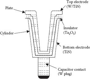
FIGURE 5.9
Schematic cross-sectional view of an MIM capacitor at 0.15 µm technology. (Adapted from “A 0.15 μm Logic Based Embedded DRAM Technology Featuring 0.425 μm2 Stacked Cell Using MIM (Metal-Insulator-Metal) Capacitor,” M. Takeuchi et al., Symp. on VLSI Techn, Dig. Tech. Papers, pp. 29–30, 2001.)
5.6.1 Ru/Ta2O5/Ru Capacitor Technology
Ta2O5 film has widely been used in SIS and MIS DRAM capacitors. Effort was also on to find a suitable metal to be used for both electrodes with Ta2O5 as dielectric. Reasons for keeping Ta2O5 in continued use were many, for example the Ta2O5 film deposition is an easier process, even at lower process temperature and has excellent step coverage. Moreover, the equipment used for Ta2O5 film deposition could also be used for economic reasons. While selecting other materials for electrodes several reports have been made available about the use of ruthenium (Ru) as electrode along with its possible drawbacks. Use of Ru electrodes has shown a distinct lowering of equivalent oxide thickness of Ta2O5 films. To study the electrical properties of a Ru/Ta2O5/Ru capacitor a sample parallel plate structure was fabricated in which Ru was deposited by sputtering [42]. Dielectric constant of the crystalline Ta2O5 in the sample structure was found to be about 65 and that was independent of the film thickness; hence, equivalent oxide thickness decreased linearly with film thickness. Leakage current density of the Ru/crystalline-Ta2O5/Ru capacitor deteriorated after forming gas annealing (FGA) process. To minimize this effect, an encapsulating barrier layer of 150 Å Al2O3 was used and found to be effective. As the storage node can be of different structures, a cylinder-type storage node shape was selected because Ru metal is easily etched by reactive ion etching (RIE). Hence, an Ru cylinder-type structure was fabricated with its storage node height being 3500 Å and the use of 120 Å thick film of crystalline Ta2O5 gave capacitance of 39 fF/cell [42].
Figure 5.10 shows the fabrication process of CVD-Ru/Ta2O5/CVD-TiN capacitor with a cylinder-type storage node for a DRAM at 0.13 μm technology level. Bottom electrode was formed using CVD process for TiN, and then Ta2O5 was deposited followed by annealing. For top electrode different materials, like sputtered-TiN, CVD-TiN, and CVD-Ru films, were used for comparison. The storage of node height was nearly 1 μm and step coverage of the Ru film was approximately 80%, covering all the exposed area of the bottom electrode resulting in maximum capacitance of 40 fF/cell. Out of the three materials used for the top electrode, CVD-Ru film was found to give the best performance in terms of leakage current stability and capacitance density [43]. A satisfactory value of 25 fF/cell was achievable even at 0.1 μm node technology with a 1 μm high storage node and toxeq = 18 Å. Hence, given capacitor structure was usable at several generations of DRAMs.
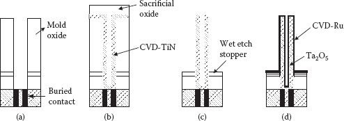
FIGURE 5.10
Process sequence to fabricate CVD-Ru/Ta2O5/CVD–TiN capacitor with cylinder-type storage node. (“Development of CVD-Ru/Ta2O5/CVD-TiN Capacitor for Multi Gigabit-Scale DRAM Generation,” W.D. Kim et al., Symp. on VLSI Tech. Dig. Tech. Papers, pp. 100–101, 2000.)
For gigabit-level DRAM capacitance, Ru has been found to be the most promising metal for electrodes because of its property of easy etching by oxygen plasma and good electrical properties. To get a good conformal CVS-Ru film and smooth morphology a novel process was developed by Won and others [44]. The technique was adapted to fabricate a concave-type of storage node of 1 μm height in 0.13 μm technology that provides a capacitance of 33.5 fF/cell with leakage current of 1 fA/cell at +1.4 V and −1.3 V.
5.6.2 (BaxSrx) TiO3 (BST)–Based Storage Capacitor
There is a practically obtainable dielectric constant limit of Ta2O5 films, hence materials with even higher dielectric constants are required. One of the better options came in the form of the use of ferroelectric materials. These ferroelectric materials have a characteristic temperature, the transition temperature To, at which the material makes a structural phase change from a polar phase (ferroelectric) to a nonpolar phase (paraelectric). The ferroelectric phase possesses spontaneous polarization, which can be reversed by an applied electric field. Because of the larger variations in the material properties that take place at the transition temperature, it is desirable to use a material whose transition temperature is outside the working temperature range of DRAMs (say 0–100°C on chip) [27].
Among the great variety of ferroelectrics, two families of materials are most promising: the lead titanate family, comprising ferroelectric phase materials (er > 100) such as PbTiO3, lead zirconate titanate (PZT) and PLZT, and the barium strontium family comprising paraelectric phase materials such as SrTiO3 (er ≈ 200) and (BaSr) TiO3 (BST, er ≈ 400) [45].
SrTiO3 and BST have given better promise for DRAM applications because they exhibit a negligible frequency dependence of the dielectric constant. In addition both BST and SrTiO3 are paraelectric at operating temperatures. There is a variety of methods of depositing BST and SrTiO3 such as sputtering, CVD, pulsed laser ablation, or metal organic deposition [27]. Among the different techniques, CVD is often considered most interesting. It has several advantages such as excellent step coverage, high deposition rate, an easy control of composition, and good thickness and composition uniformities over large-size wafers.
(Ba0.5Sr0.5) TiO3 was first utilized in a practical stacked capacitor for a 256 Mbit DRAM in 1991 [45]. One of the reasons for BST usage was that its composition was easy; hence, it was expected that its electrical characteristics would be stable. Selected electrode material was Pt mainly because of its resistance to oxidation. However, it also needed a Ta film under Pt to prevent its contamination by Si at the electrode contact. Hence 50 nm layers each of Ta and Pt were sputtered and then a 100 nm thick layer of BST was deposited at 650°C by RF-magnetron sputtering. Along with a sidewall of SiO2, 100 nm thick TiN top electrode was sputtered. For a stacked cell area of 0.5 μm2, calculated value of the capacitor was 20 fF with dielectric thickness of 100 nm. A large number of reports are now available which use BST as dielectric with decreasing oxide equivalent thickness. A few of these have been summarized in Table 5.2, containing BST film thickness, electrodes metals used, leakage current and capacitance density realized [46, 47, 48, 49,50, 51, 52 and 53] and some of the sketches of the realizations are shown in Figure 5.11(a–f). At 0.8 μm technology a 4 Mbit DRAM was fabricated, in which BST film thickness was between 50 to 100 nm, which was deposited through sputtering providing toxeq between 0.67 to 1.2 nm. Storage node material was again Pt, of course with a diffusion barrier on a p-doped poly-Si plug [47]. Soon advances were made in DRAM density in gigabit range using BST. In one such report toxeq of 0.59 nm was obtained by ECR MOCVD in BST-based stacked capacitor [48]. It employed bottom electrode of 50 nm Ti and 50 nm TiN through dc-sputtering, and RTA treatment converted Ti to TiSix salicide layer, which reduced contact resistance between TiN and poly-Si. Layers of Ru (50–100 nm) and RuO2 (350–500 nm) were formed so that TiN surface is not oxidized. (Ba0.4Sr0.6) TiO3 thin layer was then laid on the storage node. Cell capacitance of 25 fF was obtained while using only 0.125 μm2 area. At 0.14 μm technology level combination of BST with Ru storage nodes became attractive and a number of gigabit DRAM were realized [49,50].
Use of BST for 4 Gbit DRAM required still lower toxeq, which was possible at higher BST deposition temperature. However, it caused lateral oxidation of TiN increasing its resistance. To prevent the lateral oxidation RuO2/Ru storage node was constructed on a TiN/TiSix/poly-Si contact plug. An 80 nm thick BST was deposited at 550°C, though thickness of BST film on RuO2/Ru storage node sidewall was 40 nm providing toxeq = 0.4 nm. Storage capacitance of 25 fF was obtained in chip area of 0.065 μm2 with 0.25 μm high storage node [51].
It may be noted that initially Pt was used for capacitor electrode but it was replaced by Ru/RuOx electrodes because Pt was difficult to etch and oxygen can readily diffuse through it; hence it needs an oxidation resistance barrier. However, with Ru electrodes leakage current density is increased and thermal stability is reduced. Hence, for multi-gigabit density level once again Pt electrode or Ru electrode with Pt encapsulation was used.
Properties of the storage electrode metal are extremely important for the proper functioning of the BST capacitor. It is already mentioned that for Pt electrode etching is difficult as it is done mostly by physical sputtering procedure. For storage nodes below 0.22 μm minimum feature size use of Pt becomes inefficient and results in loss of electrode area, and, hence, it is no more suitable for the realization of memory cell capacitance [53]. Another serious issue is the barrier layer between polysilicon plug and metal storage electrode. Sometimes misalignment leads to a direct touch between BST layer and the barrier layer such as TiN or TiSiN, and it causes low Schottky barrier-generated large dielectric leakage current; it needs fixation. As shown in Figure 5.11(f) the problem is solved through the development of a recessed barrier layer with SiN spacer and Pt-encapsulated Ru storage node. Since etching of Pt electrode is almost impractical beyond 0.13 μm, Ru electrode is used often but rough surface of Ru electrode leads to larger leakage current. It is for this reason that the Ru electrode is encapsulated by a Pt layer [53].
Brief Descriptions of BST Capacitors
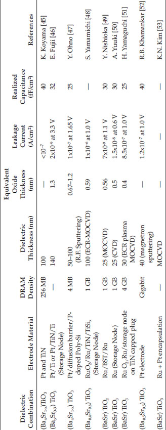
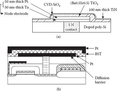
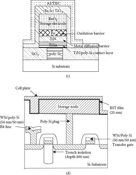
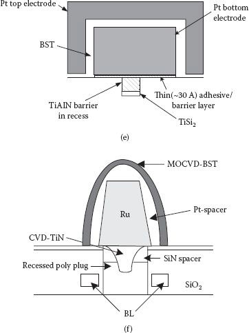
FIGURE 5.11
(a) BST based stacked capacitor fabrication. (Redrawn from K. Koyama et al., “A Stacked Capacitor with (BaxSri-x) TiO3 for 256 M DRAM,” IEDM Tech. Dig., pp. 823–826, 1991.) (b) Part of the cross-section of the memory cell having storage capacitor with BST Film. (Modified from Y. Ohno et al., “A Memory Cell Capacitor with BaxSr1-x TiO3 (BST) Film for Advanced DRAMs,” Symp. VLSI Tech. Dig. Tech. Papers, pp. 149–150, 1994.) (c) Schematic view of the capacitor structure with RuO2/Ru/TiN/TiSix storage node. (From S. Yamamichi et al., “An ECR MOCVD (Ba, Sr) TiO3 Based Stacked Capacitor Technology with RuO2/Ru/TiN/TiSix Storage Nodes for Gbit-Scale DRAMs,” IEDM Tech. Dig., pp. 119–122, 1995.) (d) Schematic cross-sectional view of DRAM memory cells with Ru/BST/Ru stacked capacitors. (Redrawn from Y. Nishioka et al., “Giga-bit Scale DRAM Cell with New Simple Ru/(Ba, Sr) TiO3/Ru Stacked Capacitor Using X-ray Lithography,” IEDM Tech. Dig., pp. 903–906, 1995.) (e) Schematic cross-section of a BST capacitor structure with Pt electrode. (Redrawn from R.B. Khamankar et al., “A Novel BST Storage Capacitor Node Technology Using Platinum Electrode for Gigabit DRAMs,” IEDM Tech. Dig., pp. 245–248, 1997.) (f) Illustration of an MIM BST capacitor with Pt-encapsulated Ru storage node. (Redrawn from K.N. Kim et al., “A DRAM Technology Using MIM BST Capacitor for 0.15 μm DRAM Generation and Beyond,” Symp. on VLSI Tech. Dig. Tech. Papers, pp. 33–34, 1999.) Pt plate and Tin electrode are deposited over the BST film.
Another paraelectric dielectric SrTiO3 has been widely believed to be a suitable candidate for fabricating DRAM capacitor in gigabit range [45,46]. A new capacitor structure using MOCVD SrTiO3 thin film on the sidewall of an RuO2/TiN storage electrode has been fabricated. A reason for selecting such a structure was that at gigabit scale sidewall surface area became larger than top surface of the storage electrode in a stacked capacitor, whereas in earlier cases only top surface of the Pt electrode was used for capacitance purpose. RIE patterning of RuO2/TiN storage node and low temperature deposition of SrTiO3, of 40 nm thick layer on 0.5 μm high node provided capacitance of 25 fF. Leakage current density was 8 × 10⁻⁷ A/cm2 at half-Vcc of +1 V [54].
Estimation of Storage Node Height for Different Feature Sizes
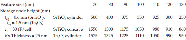
Height of storage node becomes important especially at gigabit density level DRAMs from the fabrication point of view. An estimate of the same has been obtained based on data shown in Table 5.3 for an (F ∗ 3F) storage node, to obtain capacitance of 30 fF/cell [55] for (1) cylindrical structure with Ta2O5 (teq ~1.5 nm), (2) concave structure with SrTiO3 (teq ~0.6 nm), and (3) cylindrical structure with SrTiO3 (teq~0.6 nm) to get a capacitance of 30 fF/cell. As obvious from the data, SrTiO3 cylindrical structure is preferable as its storage node height is lower than 500 nm even at 0.1 μm technology level. A cylindrical CVD-Ru/SrTiO3/CVD-Ru capacitor was successfully realized with storage node height of 300 nm and using cell area of 0.31 μm2. A 22 nm thick SrTiO3 layer provided 18 fF/cell capacitance with leakage current of < 0.1 fA/cell at ± 0.7 V [55].
5.6.3 HfO2-Based Capacitor Technology
In the search for high-k materials for memories, although having different characteristics, HfO2-based materials and Al2O3 dielectrics have also been used. ALO dielectrics have very high conduction band offset (CBO) value (2.5 eV) but relative low dielectric constant (~9), whereas HfO2 dielectric have high dielectric constant (~25) but a little lower CBO value (1.5 eV). ALO has been used mostly in trench capacitor as given in Section 5.5 or in conjunction with HfO2; only a few examples are available using ALO other than for MIM capacitors for high-density DRAMs because of its low dielectric constant in comparison to other materials. A few examples using HfO2 and AHO (Al2O3/HfO2) are discussed below in brief.
An MIM capacitor using HfO2 as dielectric was developed for the first time within a maximum temperature of 200°C (the maximum temperature of 200°C is very compatible with Cu and low permittivity interconnect technology) [56]. An HfO2 film of 56 nm was deposited on substrate by ablating Hf target in O3 ambient and then Al was deposited as the top electrode. Dielectric constant was around 18.5 and high capacitance density of 3.0 fF/μm2 with a leakage current of 2 × 10⁻⁹ A/Cm2 at 3.0 V. Many of the MIM capacitors using HfO2 have been used in silicon RF and mixed-signal IC applications. For such applications capacitor voltage linearity is very important; for the 56 nm HfO2 MIM capacitor, obtained parameters meet the requirements of the ITRS Roadmap 2001 [57].
An MIM capacitor compatible with back end of the line was fabricated in which an HfO2 film was deposited using ALD at 300°C and annealing was done at 400°C. Samples of the capacitor were fabricated with varying thickness to study its effect on capacitance density, frequency dispersion, voltage coefficient of capacitance (VCC), and leakage current [58]. The results are shown in Table 5.4 (VCC for 1 MHz only). The fact that HfO2 capacitor has nearly the same and small frequency dispersion with thickness variation of HfO2, it makes it suitable dielectric for DRAMs.
Dependence of Capacitance Parameters on HfO2 Film Thickness
HfO2 Film Thickness (nm) |
Capacitance Density (fF/μm2) |
Leakage Current at Room Temp. (10–8 A/Cm2) |
For Vcc′, C(V) = (αV2 + βV + 1) |
|
α |
β |
|||
30 |
5.0 |
2.1 |
238 |
206 |
20 |
~9.0 |
3.1 |
450 |
260 |
10 |
13.0 |
5.95 |
831 |
607 |
A cylindrical TiN/HfO2/TiN capacitor applicable to 70 nm generation DRAM was developed for the first time in which HfO2 film was deposited by ALD using Hf (NEtMe) as precursor and O2 plasma as a reactant [59]. MOCVD TiN was used as top electrode. It was observed that leakage current strongly depended on the film deposition temperature. With 13 Å toxeq, leakage current was stable at 0.1 μA/cm2 at 1.5 V and 85°C when the film was deposited at 300°C.
HSG-merged Al2O3/HfO2 (AHO) capacitor technique was introduced in 2005 [60]; however, getting uniform capacitance over full area of wafer, without any capacitor-related failure, proved to be difficult. Reliable mass production was not possible using this technique. S.G. Kim and others reported a fully integrated 512 Mbit DRAM with HSG-merged-AHO cylinder capacitor in 2006 [61]. The technique used reverse HSG one cylinder storage node (RHOCS) and AHO capacitor process as RHOCS process did not decrease the space between the storage nodes. A comparison is illustrated in Figure 5.12 between RHOCS and conventional double HSG one-cylinder storage node (DHOCS) in which HSG is grown on both inner and outer sidewalls of the cylinder by forming HSG after lift-off process. In RHOCS scheme HSG is grown on only the inner sidewall of the cylinder by forming HSG after deposition of storage node material. In the proposed scheme AHO bilayer is implemented to combine the good points of the two dielectrics, that is, high dielectric constant of HfO2 and higher conduction band offset (CBO) of ALO.
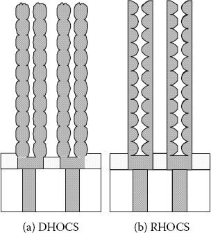
FIGURE 5.12
Comparison between (a) DHOCS, and (b) RHOCS. (Adapted from “Fully Integrated 512 Mb DRAMs with HSG-Merged-AHO Cylinder Capacitor”, S.G. Kim et al., Solid-State Electronics, 50, pp. 1030–1034, 2006.)
As predicted in earlier works, improved electrical characteristics and retention time were achieved in the fabricated DRAM in 110 nm technology without any capacitor-related leakage current failure. It was expected that the technology would be used in sub-100 nm scale.
Leakage current of the DRAM capacitor has to be equal to or less than 0.1 μA/cm2, irrespective of the equivalent oxide thickness of the capacitor. It was expected that for keeping constant EOT the use of higher permittivity materials will lead to a physically thicker dielectric film, and it would result in lower leakage current; however, that is not so. Investigation was done in terms of tunneling barrier, or in other words leakage current, work function, and applied voltage at a constant equivalent oxide thickness. It was concluded from the study that high permittivity value is effective only with large work function or at small voltage [62]. Experimental verification was done on a TiN/Hf/ALO/TiN capacitor, which with an EOT of 0.7 nm was having a leakage current of 0.08 μA/cm2 at 1 V. However, level of leakage was achieved only when Al2O3 was inserted at the bottom of the dielectric to suppress the interfacial increase in EOT. In addition Al2O3 was also inserted in the bulk HfO2 to increase the bulk permittivity. Hence a MIM capacitor with HfO2 and TiN as dielectric material combination was claimed to be one of the most promising combinations for DRAM.
5.6.4 ZrO2-Based DRAM Capacitor
As the minimum feature size comes down with each DRAM generation, fabrication of the storage capacitor for the realization of 25 fF/cell capacitance faces new challenges. As illustrated in Figure 5.13, for the design rules between 45 nm to 50 nm, required equivalent oxide thickness has to be between ~6 to 8 Å with a storage node height of 1.3 μm [63]. It was not possible to get required capacitance density at 45 nm technology level with already in-use materials like HfO2/Al2O3 stack and HfxAlyOz [64]. ZrO2 has been investigated in this respect and results have been very encouraging. Dielectric constant in the range of 15 to 18 has been achieved with good thermal stability, excellent conformality, and large band-gap [65]. ZrO2 films deposited on planar Si (100) wafers and patterned amorphous Si cylinders by RTCVD process give good conformal coverage over high aspect ratio. Properties of ZrO2 were utilized in the form of a single ZrO2 layer using atomic layer deposition in a 50 nm technology DRAM in a planar type of capacitor [66]. This simple TiN/ZrO2/TiN structure had a limitation of poor leakage current for negative bias and hence could not be easily deployed in DRAM structure. Dielectric film structure from ZrO2 and Al2O3 was then fabricated which is easily extendable to 45 nm node level [63]. A ZrO2/Al2O3/ZrO2 dielectric contains tetragonal ZrO2 and amorphous Al2O3, where ZrO2 film is deposited from Zr (NEtMe)4 as precursor and ozone as oxidant by ALD process. It was observed that compared to HfO2/Al2O3/HfO2, its capacitor value was nearly 25% higher. Equivalent oxide thickness (EOT) of ~6.3 Å could be obtained when the dielectric thickness was 32 angstroms, while keeping the leakage within bounds of 1 fA/cell at ± 1 V.
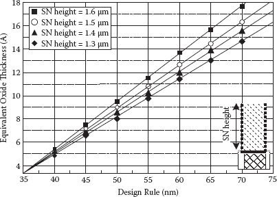
FIGURE 5.13
Required equivalent oxide thickness values for few design rules. (“Development of New TiN/ZrO2/Al2O3/ZrO2/TiN Capacitors Extendable to 45 nm Generation DRAMs Replacing HfO2 based Dielectric,” D-S. Kil et al., Symp. on VLSI Techn. Dig. Tech. Papers, pp. 38–39, 2006.)
For stacked capacitors one manufacturability requirement is to keep aspect ratio (AR) for contact and vias nearly the same at all generations. For a selected AR of 7, required EOT and height of the cylindrical capacitor for different technology levels between 45 nm and 90 nm have been shown [67], which suggests that for a 45 nm eDRAM EOT below 1 nm is needed with capacitor height being 300 nm. The basic structure of TiN/ZrO2/TiN eDRAM fabricated at 65 nm design rule is shown in Figure 5.14. The ZrO2 film was deposited using ALD process at 275°C and 10 nm thick TiN films were deposited at 400°C by ALD to form top and bottom electrodes. It is observed that even with an EOT less than 8 Å, leakage was less than 15 nA/cm2 at ± 1.0 volt (within 1 fA/cell at 125°C), which is better than that of EOT = 19 Å of Al2O3. Results shown by the process predict good manufacturability for 45 nm eDRAM technology.
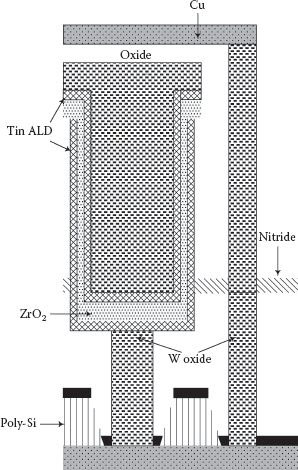
FIGURE 5.14
Schematic of a CUB embedded DRAM with TZT stacked capacitor. (Modifed from “Highly Reliable TiN/ZrO2/TiN 3D Stacked Capacitors for 45 nm Embedded DRAM Technologies,” A. Barthelot et al., Solid State Research Conf. (ESSDERC), pp. 343–346, 2006.)
MIM capacitors having dielectrics of capacitance equivalent thickness (CET) ~ 0.9 nm were manufactured for DRAMs in 2009, and further reduction in the physical thickness of the oxide and reduction in CET, while keeping the leakage current density of <1 fA/cell or 1 × 10⁻⁸ to 1 × 10⁻⁷ A/Cm2 was needed [68]. A TiN/ZrO2/TiAl MIM capacitor using a new zirconium precursor ZrD-04 was developed to satisfy the requirement of ref. [68] and [69]. On an n+ type Si substrate, a layer of TiN metal of nearly 10 nm is formed through CVD and ~7–8 nm thick ZrO2 film is deposited using ALD process at 275°C. For increasing the dielectric value without significantly increasing the leakage current premetallization rapid thermal annealing (RTP) is done at either 400°C, 500°C, or 600°C. Obtained dielectric value after RTP process is 22.5 ± 1.5 to 32 ± 5 while leakage current is still below 1 × 10⁻⁸ – 1 × 10⁻⁷ A/cm2 at 1 V.
HfO2-and ZrO2-based high-permittivity dielectrics have been used for the fabrication of MIM capacitors with satisfactory electrical performance [70]. Formation of ZrO2/Al2O3/ZrO2 prevents crystallization during deposition helping in reducing leakage [63]. However, even these high dielectric value materials shall not be adequate to the meet the challenge of fabricating DRAM capacitor with further reduced features, mainly on account of not meeting the leakage current specifications.
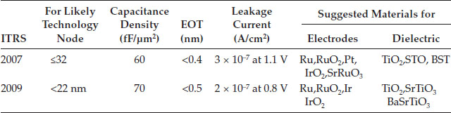
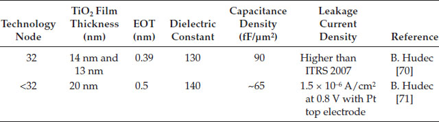
To maintain the downward scaling of DRAM capacitor, Table 5.5 shows the requirements/suggestions as given by the International Technology Roadmaps for Semiconductors (ITRS). Use of suggested dielectrics with permittivity more than 100 becomes necessary. However, these materials have lower band gaps (~3.2 eV), which may affect leakage current. TiO2 as dielectric material and RuO2 for the electrodes have been selected in two reports on the fabrication of advance MIM capacitors [71,72]. TiO2 has been chosen because of its very high permittivity of 90 to 170 in its rutile phase, though high-temperature post-deposition annealing at nearly 800°C is needed to obtain pure rutile. Pretreatment of the Ru electrode by O3 results in a thin RuO2 film which works as a seed layer for TiO2 rutile phase growth at only 250°C. In these two reports, obtained characteristics of the fabricated MIM capacitors are given in Table 5.6. Unfortunately leakage current density is higher than desired. It comes under some control with Pt as top electrode instead of RuO2. SrTiO3 (STO), mentioned as an alternative in Table 5.6 is also a promising material for DRAM capacitor. However, much work has not been done on such capacitor fabrications. ALD STO using Sr (thd)2 as precursor for Sr has been reported using metal electrodes of Ru and Pt with promising results [73,74]. Reported process could not use TiN for electrodes, as high temperature deposition or annealing was necessary in oxidizing ambient. Using another precursor and controlling the deposition variables, composition, and post-deposition processing, combination of STO and TiN has also been given [75]. New precursor was chosen as Sr (t-Bu3Cp)2, H2O, and Ti (OCH3)4, and by changing the Sr and Ti precursors’ pulse sequence, STO layer of wide compositional variety was deposited by ALD. Conformal deposition of STO in high aspect ratio is guaranteed in the process. Crystallization of sub-10 nm standard composition and Sr-rich films after 1 minute anneal in N2 at 550°C was practically available as observed in the cross-section TEM figure in Ref. [75]. For Pt/STO/ALD/TiN MIM capacitors, where STO was annealed for crystallization, provided EOT ~0.49 nm for 7.5 nm Sr-rich film and EOT = 0.69 nm for a 9 nm standard film. Leakage current was 3.5 × 10⁻⁷ A/cm2 at + 1 V and 8.9 × 10⁻⁷ A/cm2 at −1 V.
Requirement/Suggestions for Advance DRAMs
Obtained Characteristics for Two RuO2/TiO3 MIM Capacitors
STO layers have been deposited by ALD using new precursors like Sr (ipr3Cp)2 (air liquid) as Sr precursors [76] and (CpMe5) Ti (OMe)3 (Cp = C5H5,Me = CH3) (air liquid) as Ti precursors [77]. High aspect ratio STO layers were grown for MIM capacitor with thickness of layer in the range of 18–30 nm [78]. The growth temperature was 250°C or 300°C and annealing was done in nitrogen at 650°C or 750°C for 10 minutes. The film composition was close to the stoichiometric Sr TiO3 films with Sr to Ti atomic ratio in the range of 0.82 to 1.10. Up to k = 210 was obtained for film thickness between 7 and 20 nm, but the leakage current was high at ~ 1 × 10⁻⁵ A/cm2. If Sr content was reduced, leakage current could be reduced, but the permittivity came down to 30. MIM capacitors using TiN and Pt as electrode and STO as dielectric were fabricated. Dielectric films grown at 300°C using ozone provided permittivity in range of 60–65. However, leakage current does not meet the set conditions and needs further study.
1. P.C. Fazan and R.R. Lee, “Thin Nitride Films on Textured Polysilicon to Increase Multimegabit DRAM Cell Charge Capacity,” IEEE Electron Device Letters, Vol. 11, no. 7, pp. 279–281, 1990.
2. L. Faraone, “Thermal SiO2 Films on n+ Polycrystalline Silicon: Electrical Conduction and Breakdown,” IEEE Trans. Electron Devices, Vol. ED-33, p. 1785, 1986.
3. Y. Ohji et al., “Reliability of Nanometer Thick Multi-layer Dielectric Films on Polycrystalline Silicon,” Proc. Int. Rel. Phys. Symp., p. 55, 1985.
4. S.M. Sze, Physics of Semiconductor Devices, 2nd ed., Wiley, 1981.
5. M. Sakao et al., “A Capacitor-Over-Bitline (COB) Cell with a Hemispherical Grain Storage Node for 64 Mb DRAMs,” IEDM, pp. 655–658, 1990.
6. T. Mine et al., “Capacitance-Enhanced Stacked Capacitor with Engraved Storage Electrode for Deep Submicron DRAMs,” Ext. Abs. 21st SSDM, p. 137, 1989.
7. Y. Hayshide et al., “Fabrication of Storage Capacitance-Enhanced Capacitors with a Rough Electrode,” Ext. Abs. 22nd SSDM, p. 869, 1990.
8. H. Watanabe et al., “A New Stacked Capacitor Structure Using Hemispherical Grain Polysilicon Electrodes,” Ext. Abs., 22nd SSDM, p. 873, 1990.
9. P. Joubert, “Pressure Dependence of in-situ Boron-Doped Silicon Films Prepared by Low Pressure Chemical Vapor Deposition,” J. Appl. Physics, Vol. 66, no. 10, pp. 4806–4811, 1989.
10. M. Yoshimaru et al., “Rugged Surface Poly-Si Electrode and Low Temperature Deposited Si3 N4 for 64 Mbit and Beyond STC DRAM Cell,” IEDM, pp. 659–661, 1990.
11. Z.A. Weinburg et al., “Ultrathin Oxide-Nitride-Oxide Films,” Appl. Phys. Lett., Vol. 57, p. 1248, 1990.
12. P.C. Fazan et al., “Ultra-thin Oxide/Nitride Dielectrics for Rugged Stacked DRAM Capacitors,” IEEE Electron Device Letters, Vol. 13, no. 2, pp. 86–88, 1992.
13. Y.K. Jun et al., “The Fabrication and Electrical Properties of Modulated Stacked Capacitor for Advanced DRAM Applications,” IEEE Electron Device Letters, Vol. 13, no. 8, pp. 430–432, Aug. 1992.
14. H. Shinriki and M. Nakata, “UV-O, and Dry-O2: Two Step Annealed Chemical Vapour-Deposited Ta2O5 Films for Storage Dielectrics of 64 Mb DRAMs,” IEEE Trans. Electron Devices, Vol. 38, p. 455, 1991.
15. P.C. Fazan et al., “A High-C Capacitor (20.4 fF/μm2) with Ultrathin CVD-Ta2O5 Films Deposited on Rugged Poly-Si for High Density DRAMs,” IEDM, pp. 263–266, 1992.
16. H. Watanabe et al., “A New Cylindrical Capacitor Using Hemispherical Grained Si (HSG-Si) for 256 Mb DRAMs,” IEDM, pp. 259–262, 1992.
17. A. Sakai et al., “Novel Seeding Method for the Growth of Polycrystalline Si Film with Hemispherical Grains,” App. Phys. Letters, Vol. 61, p. 159, 1992.
18. H. Watanabe et al., “Hemispherical Grained Si Formation on In-Situ Phosphorus Doped Amorphous-Si Electrode for 256 Mb DRAMs Capacitor,” IEEE Trans. Electron Devices, Vol. 42, no. 7, pp. 1247–1253, 1995.
19. H. Ogihara et al., “Double-Sided Rugged Poly-Si FIN STC (Stacked Capacitor Cell) Technology for High Density DRAMs,” 52nd Device Research Conference, pp. 53–54, 1994.
20. A. Ils et al., “Investigation of the Formation Mechanism of Hemispherical Grained Silicon (HSG-Si) on Undoped and Doped Amorphous Silicon for DRAM Applications,” Proc. 29th European Solid State Device Research Conf., pp. 232–235, 1999.
21. Akira Sakai et al., “Growth Kinetics of Si Hemispherical Grains on Clean Amorphous-Si Surface,” J. Vacc. Sci. Technol. A, Vol. 11, no. 6, Nov./Dec., 1993.
22. A. Banerjee et al., “Morphology and Integration of Rough Polycrystalline Silicon Films for DRAM Storage Cell Applications,” J. Electrochem. Soc., Vol. 146, no. 6, pp. 2289–2293, 1999.
23. S. Kamiyama et al., “Ultra-Thin TiN/Ta2O5/W Capacitor Technology for 1 G Bit DRAM,” IEDM, pp. 49–52, 1993.
24. K. Kamiyama et al., “High Reliable 2.5 nm Ta2O5 Capacitor Process Technology for 256 Mbit DRAMs,” IEDM, Tech. Digest, p. 455, 1991.
25. K.W. Kwon et al., “Ta2O5 Capacitors for 1 G bit DRAM and Beyond,” IEDM, pp. 835–838, 1994.
26. A. Ishitanai et al., “Trends in Capacitor Dielectrics for DRAMs,” IEICE Trans. of Electronics, Vol. E.76-C, no. 11, pp. 1564–1581, 1983.
27. K.S. Tang, W.S. Lau, and G.S. Samudra, “Trends in DRAM Dielectrics,” Circuit and Devices, pp. 27–34, May, 1997.
28. M. Saitoh et al., “Electrical Properties of Thin Ta2O5 Films Grown by Chemical Vapour Deposition,” IEDM, pp. 680–683, 1986.
29. K. Kwon et al., “Thermally Robust Ta2O5 Capacitor for the 256-Mbit DRAM,” IEEE Trans. Electron Devices, Vol. 43, no. 6, pp. 919–923, 1996.
30. T. Kaga et al., “A 0.29 μm2 MIM-CROWN Cell and Process Technologies for 1-Gigabit DRAMs,” IEDM, pp. 927–929, 1994.
31. S. Kamiyamama et al., “Highly Reliable MIM Capacitor Technology Using Low Pressure CVD-WN Cylinder Storage-Node for 0.12 μm-Scale Embedded DRAM,” VLSI Techn. Dig. Tech. Papers, pp. 39–40, 1999.
32. I. Yamamoto et al., “Low-Temperature Metal/ON/HSG-Cylinder Capacitor Process for High Density Embedded DRAMs,” Symp. on VLSI Tech., pp. 157–158, 1999.
33. S. Saida et al., “Embedded Trench DRAMs for Sub-0.10 μm Generation by Using Hemispherical-Grain Technique and LOCOS Collar Process,” Proc. Int. Symp. on Semiconductor Manufacturing, pp. 177–180, 2000.
34. H. Ishiuchi et al., “Embedded DRAM Technologies,” Proc. of the IEDM, pp. 33–36, 1997.
35. T. Ozaki et al., “0.228 μm2 Trench Cell Technologies with Bottle-shaped Capacitor for 1 G bit DRAMs,” Proc. of the IEDM, pp. 661–664, 1995.
36. M. Gutsche et al., “Capacitance Enhancement Techniques for Sub-100 nm Trench DRAMs,” IEDM, pp. 411–414, 2001.
37. H. Seidl et al., “A Fully Integrated Al2O3 Trench Capacitor DRAM for Sub-100 nm Technology,” IEDM, pp. 839–842, 2002.
38. Jörn Lützen et al., “Integration of Capacitor for Sub-100-nm DRAM Trench Technology,” Symposium on VLSI Tech. Dig. Technical Papers, pp. 178–179, 2002.
39. H. Akatsu et al., “A Highly Manufacturable 110 nm DRAM Technology with 8 F2 vertical Transistor Cell for 1 Gb and Beyond,” Symp. VLSI Techn. Dig. of Technical Papers, pp. 52–53, 2002.
40. M. Hamada et al., “A High-Performance 0.18 μm Merged DRAM/Logic Technology Featuring 0.45 μm2 Stacked Capacitor Cell,” IEDM Tech. Dig., pp. 45–48, 1999.
41. M. Takeuchi et al., “A 0.15 μm Logic Based Embedded DRAM Technology Featuring 0.425 μm2 Stacked Cell Using MIM (Metal-Insulator-Metal) Capacitor,” Symp. VLSI Techn, Dig. Tech. Papers, pp. 29–30, 2001.
42. J.-W. Kim et al., “Development of Ru/Ta2O5/Ru Capacitor Technology for Giga-Scale DRAMs,” IEDM Tech. Dig., pp. 793–796, 1999.
43. W.D. Kim et al., “Development of CVD-Ru/Ta2O5/CVD-TiN Capacitor for Multi Gigabit-Scale DRAM Generation,” Symp. VLSI Tech. Dig. Tech. Papers, pp. 100–101, 2000.
44. S.-J. Won et al., “Conformal CVD-Ruthenium Process for MIM Capacitor in Giga-bit DRAMs,” IEDM Tech. Dig., pp. 789–792, 2000.
45. K. Koyama et al., “A Stacked Capacitor with (BaxSri-x) TiO3 for 256 M DRAM,” IEDM Tech. Dig., pp. 823–826, 1991.
46. E. Fujii et al., “ULSI DRAM Technology with Ba0.7Sr0.3 TiO3 Film of 1.3 nm Equivalent SiO2 Thickness and 10–9A/Cm2 Leakage Current,” IEDM Tech. Dig., pp. 267–269, 1992.
47. Y. Ohno et al., “A Memory Cell Capacitor with BaxSr1-x TiO3 (BST) Film for Advanced DRAMs,” Symp. VLSI Tech. Dig. Tech. Papers, pp. 149–150, 1994.
48. S. Yamamichi et al., “An ECR MOCVD (Ba, Sr) TiO3 Based Stacked Capacitor Technology with RuO2/Ru/TiN/TiSix Storage Nodes for Gbit-Scale DRAMs,” IEDM Tech. Dig., pp. 119–122, 1995.
49. Y. Nishioka et al., “Giga-bit Scale DRAM Cell with New Simple Ru/(Ba, Sr) TiO3/Ru Stacked Capacitor Using X-ray Lithography,” IEDM Tech. Dig., pp. 903–906, 1995.
50. A. Yuuki et al., “Novel Stacked Capacitor Technology for 1 Gbit DRAMs with CVD-(Ba, Sr) TiO3 Thin Films on a Thick Storage Node of Ru,” IEDM Tech. Dig., pp. 115–118, 1995.
51. H. Yamaguchi et al., “A Stacked Capacitor with an MOCVD-(Ba, Sr) TiO3 Film and a RuO2/Ru Storage Node on a TiN-Capped Plug for 4 Gbit DRAMs and Beyond,” IEDM Tech. Dig., pp. 675–678, 1996.
52. R.B. Khamankar et al., “A Novel BST Storage Capacitor Node Technology Using Platinum Electrode for Gigabit DRAMs,” IEDM Tech. Dig., pp. 245–248, 1997.
53. K.N. Kim et al., “A DRAM Technology Using MIM BST Capacitor for 0.15 μm DRAM Generation and Beyond,” Symp. on VLSI Tech. Dig. Tech. Papers, pp. 33–34, 1999.
54. P.-Y. Lesaicherro et al., “A Gbit-Scale DRAM Stacked Capacitor Technology with ECR MOCVD SrTiO3 and RIE Patterned RuO2/TiN Storage Nodes,” IEDM Tech. Dig., pp. 831–834, 1994.
55. C.M. Chu et al., “Cylindrical Ru/SrTiO3/Ru Capacitor Technology for 0.11 μm Generation DRAM,” Symp. VLSI Techn. Dig. Tech. Papers, pp. 43–44, 2001
56. H. Hu et al., “A High Performance MIM Capacitor Using HfO2 Dielectrics,” IEEE Electr. Dev. Letters, Vol. 23, pp. 514–516, 2002.
57. The International Technology Roadmap for Semiconductors, Semicond. Ind. Assoc., 2001.
58. X. Yu et al., “A High-Density MIM Capacitor (13 fF/μm2) Using ALD HfO2 Dielectrics,” IEEE Electron Device Letters, Vol. 24, pp. 63–65, 2003.
59. S.-H. Oh et al., “TiN/HfO2/Tin Capacitor Technology Applicable to 70 nm Generation DRAMs,” Symp. on VLSI Techn. Dig. Tech. Papers, pp. 73–74, 2003.
60. S.G. Kim et al., “Improved Electrical Characteristics and Retention Time of DRAMs Using HSG-Merged,” AHO Cylinder Capacitor,” Int. Semiconductor Dev. Research Symp., pp. 113–114, 2005.
61. S.G. Kim et al., “Fully Integrated 512 Mb DRAMs with HSG-Merged-AHO Cylinder Capacitor,” Solid-State Electronics, no. 50, pp. 1030–1034, 2006.
62. N. Mise et al., “Theoretical Screening of Candidate Materials for DRAM Capacitors and Experimental Demonstration of a Cubic Hafnia MIM Capacitor,” IEEE Trans. Electr. Dev., Vol. 57, pp. 2080–2082, 2010.
63. D.-S. Kil et al., “Development of New TiN/ZrO2/Al2O3/ZrO2/TiN Capacitors Extendable to 45 nm Generation DRAMs Replacing HfO2 Based Dielectric,” Symp. VLSI Techn. Dig. Tech. Papers, pp. 38–39, 2006.
64. D.-S. Kil et al., “Development of Highly Robust Nano-mixed Hfx AlyOz Dielectrics for TiN/Hfx AlyOz/TiN Capacitor Applicable to 65 nm Generation DRAM,” VLSI Tech. Dig. Tech. Papers, pp. 126–127, 2004.
65. J.P. Chang and Y.-S. Lin, “Highly Confirmal ZrO2 Deposition for Dynamic Random Access Memory Application,” Journal of Applied Physics, Vol. 90, pp. 2964–2969, 2001.
66. K.R. Yoon et al., “Extended Abstracts,” SSDM, p. 188, 2005.
67. A. Barthelot et al., “Highly Reliable TiN/ZrO2/TiN 3D Stacked Capacitors for 45 nm Embedded DRAM Technologies,” Solid State Research Conf. (ESSDERC), pp. 343–346, 2006.
68. “The International Technology Roadmap for Semiconductors,” Process Integration, Devices and Structures, pp. 29–35, 2007.
69. S. Mongham et al., “TiN/ZrO2/Ti/Al Metal-Insulator-Metal Capacitors with Subnanometer CET Using ALD-Deposited ZrO2 for DRAM Applications,” IEEE Electr. Dev. Letters, Vol. 30, pp. 219–221, 2009.
70. T.S. Böseke et al., “Stabilization of Higher-k Tetragonal HfO2 by SiO2 Admixture Enabling Thermally Stable Metal-Insulator-Metal Capacitors,” Appl. Phys. Lett., Vol. 91, pp. 072902 (1–3), 2007.
71. B. Hudec et al., “Low Equivalent Oxide Thickness Metal/Insulator/Metal Structures for DRAM Applications,” 7th Int. Conf. on Adv. Semiconductor Dev. and μ-Systems, pp. 123–124, 2008.
72. B. Hudec et al., “RuO2/TiO2 Based MIM Capacitor for DRAM Applications,” Adv. Semiconductor Devi. and Microsystems, pp. 341–344, 2010.
73. S.-W. Lee et al., “Enhanced Electrical Property of SrTiO3 Thin Film Grown by Atomic Layer Deposition at High Temperature for Dynamic Random Access Memory Applications,” Appl. Phys. Lett., Vol. 29, p. 222903–222913, 2008.
74. O.S. Kwon et al., “Atomic Layer Deposition and Electrical Properties of SrTiO3 Thin Films Grown Using Sr (C11H19O2)2, Ti (OC3H7)4 and H2O7,” J. Electron. Soc., Vol. 154, p. 127, 2007.
75. N. Menou et al., “0.5 μm EOT Low Leakage ALD SrTiO3 on TiN MIM Capacitors for DRAM Applications,” IEDM, pp. 1–4, 2008.
76. M. Rose et al., “Atomic Layer Deposition of Titanium Dioxide Thin Films from Cp*Ti (OMe) and Ozone,” J. Phys.-Chem, C., Vol. 113, pp. 21825–21830, 2009.
77. M. Vehkamaki et al., “Growth of SrTiO3 and BaTiO3 Thin Films by Atomic Layer Deposition,” Electrochem. Solid-State Lett., Vol. 2, pp. 504–506, 1999.
78. H. Garcia et al., “Characterization of SrTiO3-based MIM Capacitors Grown by Using Different Precursors and Growth Temperature,” Proc. 8th Spanish Conf. Electr. Dev. (CDE’2011), 2011.