Shrinking technology has remained the most important priority for DRAM development. At the same time it is responsible for most of the challenges. When the requirement of small area enforced adoption of the three-dimensional cell instead of the planar cell, technological advancements followed in parallel for the trench cells as well as for the stacked cells (and their variations), having their own advantages and limitations. From a topological point of view, the trench cell DRAM was found to be better as its capacitor was below the silicon surface. However, increase in DRAM density required a deeper trench for realizing sufficient storage capacitance; a bit impractical. The feature of low thermal budget fabrication owing to capacitor formation at early stage is also an advantage; hence, trench cell became more appropriate for merged DRAM where density might not be the first priority. However, not altogether replacing trench cells, stacked cell structures have found favor at the gigabit level. But even these kinds of cells are facing many challenges with decreases in technology scale. One of the significant technology changes came in the form of capacitor-over-bit-line (COB) structure from the capacitor-under-bit-line (CUB) structure, to get certain minimum cell capacitance in the stacked capacitor cells. Though to get advantages offered by the COB structure, certain difficulties in fabrication had to be solved. Steps taken in this direction that enhance its suitability for high-density DRAMs shall be discussed.
To sustain shrinking, technology’s first requirement was having the basic cell components (the access transistor and the storage capacitor) confined to ever-decreasing projected chip area, while keeping/improving performance that satisfied set standards in terms of speed, power consumption, data retention time, and so on. At the same time complexities in process fabrication were also to be eased and overall chip size was to remain within practical/economical/yield limits. The following simple relation can work as a guideline:
where F and N are the minimum feature size and number of cells, respectively, for a folded bit-line array structure and the array efficiency is taken as 65%. In addition to pursuing open bit-line structure (with minimum cell size of 6 F2), technological advancements are also being continuously made for realizing < 4 F2 cell size either using vertical [1] or stacked surrounding gate (S-SGT) transistor [2] or three-dimensional stacking of DRAMs [3]. Smaller cell size directly requires small size access transistor while maintaining its drive, keeping Ioff/Ion within prescribed limits and overcoming secondary effects (becoming more dominant) with F becoming smaller like short channel effect (SCE), DIBL, GIDL, and so on. The storage capacitor is the second most important component directly affected by the shrinking technology and needs adequate attention. Though capacitor in planar form is always preferred, other forms like trench, stacked, or vertical (with variations) have been investigated. SiO2, which was the basic dielectric, could not remain viable and hence was replaced by Si3N4 (or layered with it), Ta2O5, and other high-k dielectrics at increasing levels of DRAM density. Enhancement in storage capacitance value was commonly achieved using grained or textured surface of storage node. Efforts were always made to reduce leakages to a minimum as it affected cell and chip design considerably.
Quadrupling of DRAM density every three years could become practically possible only through technological advancements in the area of lithography, isolation, and etch process. Better resolution, suppression of proximity effects using optimization technique and minimization of mask alignment errors became essential. Solutions were needed for reducing depth of focus for resolution enhancements. Wavelength in optical lithography was reduced from 468 nm to 365 nm to 248 nm and then to 193 nm. Efforts are now on to see how 13.5 nm lithography could be put in practical use. Advancements in lithography were not only essential for the realization of small size transistor and storage capacitor but their contacts with word line and bit line through tiny holes/vias became extremely important. Thin word lines and bit lines and other connecting wire strips of ever-decreasing thickness with small pitch were not possible without lithographic and etching process advancements. Isolation technique and lithography advancements are related and their combination helps reducing cell size, as isolation technique controls the process margin and compensates for alignment errors. At small technology nodes those margins become extremely important and sometimes result in open circuiting thin wires or short circuiting small gaps.
With advancements in device technology and cell capacitor, performance started to be affected with bottlenecks in the support circuit technology. Chip areas occupied by the support transistors in CMOS technology and its leakage current and power consumption became important. All parasitic capacitance and resistance of the WLs and BLs and other interconnects needed to be reduced, which meant usage of better conductivity wires and low-dialectic inter-layer material development. Better connection technology became essential for all such wires. Hence, discussion in the following sections is mainly on the development in the area of memory cell transistor and storage capacitor technology, lithography technology including isolation techniques, cell connection technology including landing pad formation and storage node contact and cell contact. Interconnect technology also forms an important component of the discussion.
Advanced cell structure era started with the realization of trench capacitor cells in which highly doped polysilicon was filled in a trench below the planar surface of the substrate, which served as one plate of storage capacitor. Thin SiO2 layer (or a composite layer with Si3N4) was thermally grown on the trench walls to act as dielectric and the storage electrode was in the substrate in the first generation of such cells. These initial attempts in three-dimensional cell design revealed quite a few limitations. It became difficult to increase DRAM density further with reduced projected area, as a deeper trench became necessary in order to realize a minimum of (say 25 fF) capacitance. Moreover as the storage electrode was a part of the substrate, chances of higher inter-cell leakage current increased in closely spaced cells. Higher level of substrate doping did reduce the thickness of depletion region, reducing inter-cell leakage current, but cells could have avalanche breakdown at in-between spacing of 0.8 μm. Starting from the corrugated capacitor cell of Sunami [4] several structures like folded capacitor cell [5], vertical capacitor cell [6], isolation merged vertical capacitor cell [7], buried isolation capacitor cell [8], and FASIC cell [9] have appeared. The aims behind all these design modifications included enhancement of capacitance with shallower trench and/or less size, reduction of leakage, and making the cell less susceptible to soft errors due to alpha particles. Description of these first-generation cells is given in Section 2.3.1 of Chapter 2.
To overcome the major problem of punch-through among closely placed cells and minimization of soft errors in increasing density DRAMs, second generation trench capacitor cell structures were developed in which the storage electrode was inside the trench and the plate electrode was on the outside of the trench. Examples of such cells, which were also called inverted trench cells, are buried storage electrode cell [10] substrate plate trench capacitor cell [11], and the stacked transistor cell [12]. These are discussed in Sections 2.6, 2.3.2.1, and 2.7, respectively. Another important development in the inverted type of trench cell came in the form of the fabrication of access transistor above the trench capacitor so as to save precious chip area. Important advance in the category is the trench transistor cell (TTC) [13] discussed in Section 2.5.
Progress of trench capacitor DRAM structures slowed down on account of difficulty in realizing deeper trench for getting sufficient capacitance in extremely reduced area. Technological advancement in fabricating deep trenches, having aspect ratio of the order of 70, was made at sub-100 nm technology nodes. In the meantime different versions of 3-D cells in the form of stacked capacitor cells (STCs) in which capacitor was fabricated above the access transistor instead of being in a trench, as described in Section 2.8, appeared to be better placed in using high permittivity dielectric in metal-insulator-metal (MIM) capacitors. The STC structure also helped in minimizing cell signal charge reduction effect which was present in earlier planar type capacitors due to the minority carriers generated in the silicon substrate. Different versions of STC cells in the form of horizontal and vertical fin structures, with varying degrees of complexity and ability to realize higher capacitance density, were fabricated. To get more capacitance per unit area STC structure was changed from capacitor-under-bit-line (CUB) to capacitor-over-bit-line (COB) for gigabit-density DRAMs, in spite of having few initial stage technological constraints. Use of self-aligned technology needed to be deployed in COB structures for fabricating landing pads and contact holes. Aspect ratio of the storage node was also to be reduced and reduction of parasitic resistance and capacitance needed sufficient attention. A few early COB structures like straight-line trench isolation and trench-gate transistor (SLIT) [14] and related technology were discussed in Section 2.8, whereas advanced COB cell structures are given in Section 3.5. MIM capacitors with different materials for top and bottom electrodes are to be used beyond 100 nm to get sufficient storage capacitance. Obtaining mechanical stability for the storage node is another important requirement for gigabit DRAMs. Two mechanically robust COB structures, LERI (learning exterminated ring-type insulator), and MESH (mechanically enhanced storage node for virtually unlimited height), are discussed in the following section.
6.3 Robust Memory Cell—Mechanical Stability of Storage Node
COB DRAM cells have proved to be suitable for DRAMs from 16 Mbit density level onwards. Different approaches have been used for enhancing cell capacitor/area and the use of cylindrical capacitor has been very prominent since the early 1990s [15]. To satisfy the requirement of at least 25 fF/cell, first MIS capacitors were used in which Ta2O5 dielectric film was introduced at 0.18 μm technology. From 0.13 μm technology node, both MIS capacitor with Ta2O5 as dielectric layer and MIM capacitor with different materials (but mostly Ru), for top and bottom electrode were used and beyond 100-nm the Ta2O5 capacitor no longer remained useful as its dielectric constant was not sufficiently high. For 0.13 μm technology, in general, cylinder-shaped storage node structure replaced BOX-shape storage node to increase the surface area of the storage node. When DRAM level improved to 0.11 μm technology, height of the cylindrical node was to be increased and its shape was also modified. The idea behind change of shape was to provide mechanical stability to the storage node to avoid cell-to-cell short or twin-bit failure.
Capacitance of a Cylindrical Capacitor as a Function of Film Thickness
Dielectric thickness (nm) |
30 |
25 |
20 |
15 |
Capacitance (fF/μm2) |
42 |
48 |
61 |
80 |
At 0.13 μm design rule stage metal/Ta2O5/metal capacitor was realized in which CVD TiN film was used for cylindrical node [16]. Cell capacitance of 40 fF/cell with leakage current of 0.1 fA/cell at ± 1 V applied voltage was achieved. Another MIM DRAM cell at 0.11 μm technology level having cylindrical electrodes with Ru was realized [17]. A two-step CVD-SrTiO3 (ST) was employed with SiO2 equivalent thickness of 0.6 nm. Table 6.1 shows the capacitance of a cylindrical capacitor as a function of SrTiO3 film thickness having storage node height of 300 nm and cell area of 0.13 μm2 with a dielectric constant of ~135.
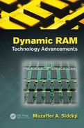
When Ta2O5 is used in MIM capacitors, best performance is obtained when electrodes are realized with Ru as its dielectric constant rises to 70 or SiO2 equivalent of 0.7 nm (Ta2O5 ~10 nm). However, there is a major practical problem of integrating three-dimensional electrodes with Ru. Formation of cylindrical bottom electrode with Ru faces two serious problems: (1) adhesion between Ru and SiO2 is very poor, causing seepage of wet etching at the interface during sacrificial SiO2 strip process and effects the collapse of cylindrical electrodes (Figure 6.1(a)), and (2) oxygen easily penetrates through Ru film, oxidizing the surface of the contact plug material (Figure 6.1(b)) resulting in some contact failures. These problems have been solved by a liner-supported cylinder (LSC) technology and a robust cylindrical electrode with Ru, which has been realized at 0.13 μm technology [18]. TiN liner is formed in the shape of a cuplike cavity and the liner acts both as adhesion layer and as oxidation barrier as illustrated in Figure 6.2. Cylinder capacitors of 550-nm height were fabricated without any collapse. Assuming that practically suitable value of aspect ratio would be less than eight, Ru electrode with LSC technology is much better than other electrode materials such as TiN, as it yields best performance of Ta2O5 and downscaling beyond 0.10 μm is feasible [18] for realizing a capacitance of 30 fF/cell.
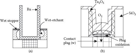
FIGURE 6.1
Difficulties in integrating Ru with cylindrical electrode. (a) Poor adhesion of Ru/SiO2; wet etchant penetrates along the interface. (b) Oxygen can penetrate Ru film to oxidize plug material during Ta2O5 formation. (Redrawn from “Linear-Supported Cylinder (LSC) Technology to realize Ru/Ta2O5/Ru for Future DRAMs,” Y. Fukuzumi et al., IEDM, pp. 793–796, 2000.)
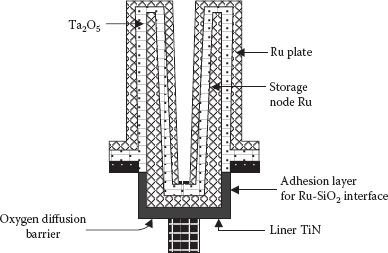
FIGURE 6.2
Schematic of a liner-supported cylinder capacitor. (Redrawn from “Linear-Supported Cylinder (LSC) Technology to Realize Ru/Ta2O5/Ru for Future DRAMs,” Y. Fukuzumi et al., IEDM, pp. 793–796, 2000.)
A 4 Gbit DRAM fabricated in 0.11 μm CMOS technology, having cell size and the chip size of 0.1 μm2 and 645 mm2, respectively, was given by K.N. Kim and others in 2001 and claimed to be the first working highest density DRAM at that time [19]. The cell used 80 nm array transistor, sub-80 nm memory cell contact, and mechanically robust capacitor by using a novel capacitor structure in which concave structure to cylindrical structure is added as shown in Figure 6.3.
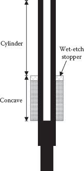
FIGURE 6.3
A capacitor fabricated using merged structure of cylinder and concave (MSCC) storage node. (Modified from “Highly Manufacturable and High Performance SDR/DDR 4 Gb DRAM,” K.N. Kim et al., VLSI Tech. Dig. Tech. Papers, pp. 7–8, 2001.)
A multistack storage node structure having enlarged bottom size of one cylindrical storage node with much stronger mechanical stability of the capacitor was realized in 2003. Capacitance of 22 fF/cell with ALD Al2O3/HfO2 dielectric film (toxeq = 2.5 nm) was realized when the capacitor height was 18000 Å. However, 30 fF/cell capacitance could be achieved using the multistack capacitor having a total height of 22000 Å, composed of 7000 Å box-shaped (BS) capacitor stack and 15000 Å cylindrical-shaped (CS) capacitor stack [20]. The COB cell was expected to be easily fabricated in 70 nm node and beyond for longer data retention time and mechanical stability of the capacitor using the multistack structure. Figure 6.4 shows the robust multistack cell capacitor composed of BS and CS capacitor. Surface area is increased by nearly 45% in this case compared to a conventional storage node.
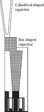
FIGURE 6.4
A robust multistack cell capacitor. (Modified from “Robust Memory Cell Capacitor Using Multistack Storage Node for High Performance in 90 nm Technology and Beyond,” J. Lee et al., Symp. VLSI Techn. Dig. Tech. Papers, pp. 57–58, 2003.)
In 2004 two mechanically robust, COB DRAM cells for 70 nm node and beyond were given: (1) a leaning exterminated ring-type insulator (LERI) [21], and (2) mechanically enhanced storage node for virtually unlimited height (MESH) [22]; both of these used conventional MIS technology without twin bit failure. The reported LERI process realized 32 fF/cell at the design rule of 82 nm and the MESH process realized 30 fF/cell with an equivalent 2.3 nm oxide thicknesses in a MIS capacitor, with required storage node height of about 2.5 μm. For 80 nm DRAM technology leaning of storage nodes severely deteriorates yield at the height of 1.6 μm. The MESH process tried to improve the process difficulties which came up during integration of LERI with one cylindrical storage node. The cross-linking MESH supporters prevent all cylinders from leaning and DRAMs with high yield and extremely low level of twin bit failures were obtained. One of the key advantages of the MESH process is that it does not need additional lithography for the support structures. For further enhancement of capacitance, HSG-Si was grown only on the surface of inner cylinder and a 15–30% capacitance gain was possible with process optimization.
6.4 DRAM Cell Transistor Technology
Fabrication of transistor in a DRAM chip occupies a central position. Along with the storage capacitor, it is replicated in the core array and affects not only the area (or cost) but its performance as well. It is therefore, always fabricated in minimum size and in NMOS technology and optimized for performance and fabrication process simplicity. On rest of the chip, transistors, though not necessarily of minimum size, are to be used in every module—for example, in sense amplifiers, row and column decoders, buffers, I/O pads, and so on—and peripheral transistors are generally fabricated in CMOS technology. Because of the requirement from the transistor and the form of utilization on the chip, memory cell transistor and the peripheral transistors are different in terms of constructional details and characteristics. Before reaching technology node of nearly 100 nm, planar, single gate, and conventionally fabricated transistors were used in memory cell and peripherals. However, even at 0.25 μm, the problems of accommodating cell transistor in a small area faced difficulties which were compounded due to the loss of active width from isolation oxide and mask alignment tolerance error. Better isolation technology in the form of shallow trench isolation has given excellent results and shall be discussed in Section 6.7. A major problem faced was a near nonscalable threshold voltage (Vth) in cell transistor, even when drain-to-source voltage was to be scaled down with reduced channel length. Generally Vth of nearly 0.7 V or more was to be used to keep sub-threshold current under control. At the same time, transistor gate voltage which had to be increased by at least a threshold-voltage drop across it (in order to retain its drivability), its gate oxide thickness had to be increased. At technology node level beyond 0.25 μm, short channel effect (SCE) and narrow width effect created considerable deviations in Vth and the deviations increased further with decreasing feature size F. One of the commonly used techniques to increase Vth (or maintain) and decrease the effects of SCE was to increase substrate doping density to more than 1018 per cm3 for gigabit-density DRAM. However, it increased leakage current and hence modifications were suggested in fabrication process like reduced doping density just below the source/drain, but a simple one-gate conventional structure was just not enough. Leakage current reductions have been attempted widely using circuit innovations and are described in Chapter 7. However, bottleneck minimization at around 100 nm nodes and beyond was done through the use of special kinds of transistors. First in line were recess channel array transistor (RCAT) and spherical RCAT [22,23] in which effective channel length was increased through recessing. These transistors discussed in Section 4.2 were found to be very useful up to at least 50 nm node technology. Double gate MOSFETs/FinFETs based on DELTA structure [25] and variations like body tied MOSFETs/bulk FinFETs, discussed in Sections 4.2, 4.3, and 4.4 were excellent replacements in sub 50 nm ranges with small Vth variation and DIBL and good SCE immunity along with process compatibility of bulk FinFETs with the conventional planar MOSFETs. Because of double gate structures these transistors were inherently providing more drive. Multichannel FET and saddle FinFET [26], discussed in Sections 4.6 and 4.8, have also shown great promise in sub-50 nm technologies with their own advantages, combining good points of RCAT as well.
In higher-density DRAMs, characteristics of MOSFETs, especially drivability decrease due to channel width decrease effect, were further improved in surrounding gate transistor (SGT) and stacked SGT in which source, drain, and gate were realized in a vertical fashion. Apart from improving transistor characteristic, it led to three-dimensional structure and was able to realize cell area per bit of less than 4 F2 as discussed in Section 4.10. Trench capacitor cells which were overshadowed by the stacked capacitor cell with advanced transistors were given a boost in the form of BEST and VERIBEST cells [27,28] at 4 Gbit/1 Gbit level using vertical pass transistor (Section 4.11). In fact, vertical transistors, in which channel length can be chosen independent of design rules, could satisfy the requirement of Ion (with double gate), while keeping Ioff < 1 fA/cell. Vertical transistor and its variations [29] have been discussed in Section 4.12 and these are found to be suitable at 30 nm level or beyond. Section 4.13 has included a brief discussion of few advanced recess FinFETs, like FET partially insulated RCAT (PiRCAT), partially insulated FinFET (PiFinFET) [30] and fin and recessed channel MOSFET (FiReFET) [31]. These advanced devices have further improved upon RCAT and FinFET for still small technology node.
Transistors used in the periphery, in general, have used simpler planar structure fabrication processes, with emphasis on keeping leakage low and higher breakdown voltage. Their channel length was generally larger by at least one generation compared to that for the cell transistors.
A minimum capacitance of 25 fF/cell has been selected as a guideline and has become a cornerstone for DRAM design as it controls not only the functionality but also its performance. Initially it was fabricated in a simple parallel plate form with the most compatible dielectric SiO2 by the side of an access transistor. However, it became a challenge with increasing DRAM density and all possible ways were adopted to fabricate it in smallest possible area and with minimum of leakage. Crown-shaped capacitor and Ta2O5 dielectric were predominantly used as the capacitor technology up to 256 Mbit DRAM (and extendible to 1 Gbit) level which has already been discussed in Section 3.4.1. Hemispherical grained surface and CVD-Ta2O5 layers with rapid thermal annealing (RTA) were also used for capacitance enhancement. Other high-k dielectrics like (BaxSr1-x) TiO3 and SrTiO3 were also under investigation at 256 Mb–1 Gbit level. Capacitors using Ta2O5 were based on (MIS) metal-insulator-polysilicon structure, where metal was used for the plate electrode and the polysilicon (heavily doped) was used for the storage node. Metals used for the plate electrode were either highly doped polysilicon/titanium nitride (TiN) or heavily doped polysilicon/tungsten nitride (WN), as these metals were better suited for the twin job of preventing oxygen escape from Ta2O5 layer and also prevented a reaction between Ta2O5 and the heavily doped polysilicon layer which itself was protecting TiN or WN from oxidation. Such MIS capacitors could not be used beyond 0.13 μm technology as sufficient capacitance could not be obtained without further thinning the Ta2O5 layer, which was practically not possible; otherwise it would have led to punch-through. Hence polysilicon was replaced by metal for the storage electrode and the structure was called MIM (metal-insulator-insulator). It helped in eliminating the native oxide on the polysilicon storage node surface and Ta2O5 could be further scaled down to improve realized capacitance. However, increase of DRAM density and variation in fabrication processes especially processing temperature, different metals for electrodes, like platinum (Pt), ruthenium (Ru), RuO2, and Ti/Sr were used. In addition, other than Ta2O5, dielectrics like Al2O5, HfO2, ZrO2, BST series, and Ti-based ones were used so that combinations of new metal electrodes and high-k dielectrics were able to realize DRAM capacitance, which not only satisfied the specifications but also became manufacturable. At 0.13 μm level Ru as metal electrode was found very useful because it could obtain a capacitance of 40 fF/cell [32] and continuation of Ta2O5 usage restricted the enhancement of fabrication cost. However, soon BST capacitor structures in large number forced Ta2O5 to be replaced. All combinations of electrode metals as mentioned above were combined with BST based capacitor at gigabit DRAM level [33,34,35,36,37,38,39,40]. A comparative statement is given in Table 6.2 about a few of these realizations. Employed technologies could give even 0.5 to 0.4 nm of equivalent oxide thickness and still leakage was under control (though at reduced voltage levels). BST was found to be extremely useful, having dielectric constant between 200 to 400; however, it faced a few serious problems. For example, BST could be crystallized only on metal electrode and barrier height between BST dielectric and metal electrode was a matter of key concern. Moreover, dielectric constant of a BST film is proportional to its thickness; hence, reducing its thickness does not provide proportional increase in capacitance.
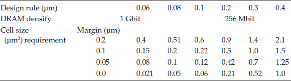
Open Bit Line DRAM Cell Size as Function of Design Rules for Different Value of Margins between Contact Hole and Adjacent Wirings
Other high-k materials based on HfO2 and Al2O3 dielectrics have been used in MIM capacitors at around 70 nm node technology. Generally, TiN was used for metal electrodes and HSG was also developed for capacitor enhancement. However, HfO2/Al2O3 stack could not be used for 50 nm node technology and ZrO2 films having dielectric constants between 15 to 18 deposited on planar Si wafers have been used. Advanced fabrication techniques allowed TiN/ZrO2/TiN eDRAMs with equivalent oxide thickness of <0.8 nm.
Use of dielectrics having k >100 becomes necessary for technology node beyond 32 nm and at the same time leakage current has to be within bound as suggested by ITRS (2007/2009). Advanced MIM capacitors using TiO3 (k 90–170) in its rutile phase has been selected, while its leakage current is controlled using Pt as top electrode instead of RuO2. ALD SrTiO3 (STO) is also a promising material, (needs precursor) with metal electrodes of Ru and Pt [41]. Obviously research and development on stable, high-k dielectrics having compatibility with a suitable metal for electrodes which keeps leakage current to minimum shall continue.
The rate of DRAM density advancement could not have been sustained without lithography technology advancements. Though the basic objective remains the same in the form of generating precise microscopic patterns in a photosensitive resist material, its practical form has continued to change over the years. A high intensity light source illuminates a mask, an image is formed on a photoresist-coated wafer through a lens, which is ultimately converted into trenches in wafer or strips of metal on silicon. Nature of light source, placement of masks, types of resists, removal of materials from wafer—all went through drastic development stages. Literature is very rich on the subject, and a good review is available in ref [42] up to 1997.
Nature of light source defines the optical resolution (R) in lithography which is related by the Rayleigh equation (R = k1λ/NA), where k1 is a proportionality factor, λ is the light wavelength, and NA is numerical aperture of the optics. The constant k1 has a limiting value of 0.25 for a single exposure and as k1 decreases, contrast is lost in the image. Memory devices like DRAM, SRAM, NAND flash, and so on, in which the layouts are highly periodic with certain fixed pitches, resolution enhancement technology (RET) is now almost always used to better the contrast in sub-micrometer technology level. Common RETs employed include off-axis illumination (OAI), phase-shift mask (PSM), and optical proximity correction (OPC), along with liquid immersion lithography and double patterning techniques.
Below 256 Mbit DRAM, i-lines and g-lines of Hg-Xe Arc lamps were used as light sources. Emission centered on 248 nm but unfortunately power available at this wavelength was very low, at the same time lithographic issues at gigabit DRAM level are different and challenging. While obtaining extremely small size patterns that are even less than the wavelength of the exposure tool, resolution, and alignment accuracy became critically important. Minimization of variations in pattern size across whole of a larger size chip became another important issue. All these requirements made it essential to use the RETs mentioned above.
In 1997, Hg i-line light sources at 365 nm were replaced with excimer lasers to satisfy volume manufacturing needs for sub 0.25 μm features in semiconductor devices. By 1995 deep ultra-violet (DUV)-grade fused silica and 248-nm resists were complete and the KrF laser became the main tool of lithography. A large number of DRAMs were manufactured not only at 0.25 μm level but at 0.15 μm [43], 0.13 μm [44,45], and even 0.11 μm level [46,47]. At 0.15 μm level, improvement of resolution and suppression of proximity effect were found to be key factors and these were obtained using illumination optimization and OPC correction, respectively. Suppression of mask error amplification was another important issue which was achieved through the introduction of a new mask making process such as thin resist and dry development process [43]. While fabricating a DRAM cell at 0.13 μm, importance of lithographic-centric cell has been emphasized for better results. Attributes for such a cell include a highly regular pattern layout, maximum use of one dimensional level and maximized contact/capacitor area [44]. Full CMP technology was developed in another 0.13 μm DRAM to continue its deployment. The use of newly developed PAOCS capacitor also helped its cause which restricted the aspect ratio of the metal contact to less than 10, which was not possible with full CMP [45].
Due to diffraction and/or process effects, projected images on the wafer appear with irregularities. Line widths appear to be narrower or wider than the design values and rounded corners become distorted. If these distortions are not corrected they can change the electrical characteristics. Optical proximity correction (OPC) methods are used to make up the distortions. Conventional methods include use of pre-computed tables showing spacing between different kinds of layout strips or through dynamically simulated final patterns. OPC corrections have invariably been used in all fabrications beyond 0.18 μm technology levels. Off-axis illumination (OAI) is another resolution enhancement method which is also almost invariably used. If incoming light is made to strike the photo mask at an oblique angle rather than perpendicularly, it is called OAI. This occurs because when light strikes the grating on the mask and is diffracted in different directions. For very small pitch, no pattern is created on the wafer; however, by making the illumination off-axis, all diffraction orders are tilted, which makes it easier for the higher diffraction orders to pass through the projection lamp and form image on the wafer.
In conventional photo masks, thickness of the transparent plate is the same throughout, whereas in shifted masks (PSM) it is not so and interference generated by phase difference is used to improve image resolution. In alternating PSMs, certain transmitting regions of the mask are made thinner or thicker, which induces a phase shift in the light passing through these regions. A suitably selected phase shift interferes with the light coming through a normal transparent region, improves contrast, and improves the resolution on the wafer. In attenuated PSMs certain opaque parts of the masks are so modified that a very small percentage of light passes through them as well. The opacity produces an interference with the light coming from transparent regions and improves the contrast. PSM has the added advantage of reducing the sensitivity to variations of feature size on the mask, which is very important for decreasing feature sizes.
A 4 Gbit DRAM at 0.11 μm technology was fabricated using KrF lithography, where maximum resolution was obtained by using OAI. However, use of hard OAI and PSM result in very small DOF margin in the peripheral area. A new scattering bar OPC pattern, shown in Figure 6.5, was developed to improve patterns and more than 0.3 μm DOF was obtained [46]. Of course full CMP was also used for DOF improvement. Another example of the continued use of the KrF lithography at 0.11 μm is the form of a 4 Gbit DRAM [47]. It uses all the performance enhancing techniques like PSM, strong OAI, OPC, and high NA exposure system. Full planarization using CMP was also done.
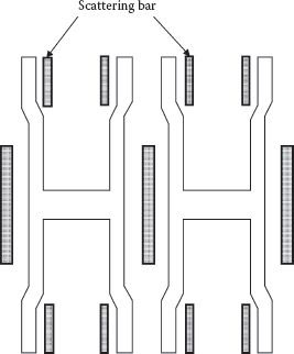
FIGURE 6.5
Layout of scattering bar pattern. (Redrawn from“Highly Manufacturable 4 Gb DRAM Using 0.11 μm DRAM Technology,” H.S. Jeong et al., IEDM Tech. Dig., pp. 353–356, 2000.)
Beyond 100 nm, DRAM fabrication had to introduce 193 nm ArF lithography; though it could have been introduced at 0.13 μm level, economical reasons forced the continued used of KrF technology along with RETs. ArF lithography has successfully been used in a big way [48,49,50,51,52,53,54] down to 45 nm minimum feature size with the support of conventional RETs and few more advanced technologies like double exposure and immersion lithography [55]. At 90 nm technology high transmittance (HT)-PSM, scattering bar OPC and strong OAI are used with ArF lithography [48], whereas at 80 nm recessed channel of the RCAT was formed with poly mask layer and chemical dry etching process [49]. For 70 nm DRAM, extreme OAI, alternated PSM, and OPC were used [50]. Along with the RETs, layout in straight lines helped in achieving a DOF >0.3 μm for all critical layers like active, gate, self-aligned-contact pad, bit line, and storage node. For a 6 F2 DRAM cell at 60 nm levels, double exposure technology (DET) was also used [51]. For enhancing the resolution DET is used extensively. A typical example is illustrated in Figure 6.6 with two masks and obtained pattern [52], and the final figure is a sum of two exposures.
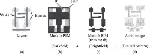
FIGURE 6.6
(a) Schematic of double-exposure phase-shift mask process. The desired pattern is decomposed into two exposure levels: (b) a dark field phase edge, and (c) bright-field trim exposure (d) the desired final image is a sum of those two exposures. (“Enhanced Resolution for Future Fabrication,” M. Fritze et al., IEEE Circuits and Device Magzine, Vol. 19, pp. 43–47, 2003.)
Numerical aperture (NA) which is the product of the sine of the maximum refraction angle and the refractive index of the medium through which light passes, decides the resolution. Up to 65 nm, final lens and wafer were separated by air gap and beyond this level resolution could not be increased, resulting in blurriness. In immersion lithography (IL), instead of air gap, highly purified water is used as medium, which increases the refractive index of the UV light at 193 nm to 1.44. Enhancement in resolution is around 30–40% which depends on the medium used. In addition, DOF is also improved around two times. Example of the use of ArF IL is given in a report [53] for the critical layer of active, word line, SAC pad, bit line, and storage node (SN) of a 56 nm DRAM. A DOF of more than 0.1 μm was obtained with IL along with the use of extreme OAI, attenuated PSM, and model-based OPC. ArF IL has also been used successfully for the critical patterns such as active, fin, word line, bit line, SN contact, and storage node even at 44 nm DRAM [54].
Water-based ArF immersion lithography has successfully printed patterns down to ~45 nm with acceptable k1 (>0.3), and NA could be extended up to 1.35. Implementation at this level did require significant OPC and lithographic friendly layouts. Further increase beyond this NA was not possible with water-based systems. The advantage of using much of the existing infrastructure helped achieve NA>1.6, which was essential for the next lithography step of 32 nm node. However, it did require new high-index final lens material, a high-index immersion liquid and high index polymer for resist formulation. Unfortunately, none of the three mentioned material developments were available even by 2008 [55]. A few other exploratory alternatives were attempted, but insufficient success forced a look for feasible alternatives: 193 nm double patterning or deep UV (λ = 13.5 nm) lithography.
There are quite a few techniques through which double patterning is applicable with the basic idea remaining same in the form of lowering k1 while keeping NA and wavelength the same [56]. As the half pitch below 45 nm is not achievable practically in a single lithographic step, the process is split over two steps. It reduces the effective value of k1 below the theoretical limit of 0.25 for the single step. One of the easier methods of conversion of the basic technique into practical fabrications is the one in which the first lithographic step is transferred into a hard mask layer by etch, and subsequent imaging and etching of a second photo resist layer. Two options are available in the process of litho-etch-litho-etch (LELE) either by double trench or double line patterning [55]. An important advantage lies in its development using the tools already available; hence, existing infrastructure could be used. Though the economic advantage gained is offset by the fact that those double exposures nearly double the lithography cost. As far as technology is concerned, main challenge in the process comes from aligning the first and second exposures. Critical dimensions are likely to be affected if the overlay automated solution, where dense layout is split into two sparser layouts and two masks, is used separately and the result is combined on a single wafer [57].
Progress in lithography is mainly due to reduction in wavelength from 436 to 365 to 248 and then to 193 nm. But adoption of new wavelength as mainstream technology becomes possible only after a considerable experience in the usage of masks, tools, resists, and so on; 193 nm technology could advance further after the applicability of four generations of tools. A wavelength of 157 nm could not be successful mainly because of the unavailability of good-quality projection lenses. For various other reasons as well, wavelengths below 157 nm could not be employed. Extreme UV (EUV) wavelength at 13.5 nm can provide major relaxation in NA and k1 and could be used for several generations in resolution extension. However, its implementation requires fulfillment of other technical and economic feasibilities as discussed in ref. [55].
Benefits of using 13.5 nm lithography are huge; if successfully implemented, benefits similar to those of optical lithography are likely to be available. For 32 nm half-pitch imaging at 0.25 NA, k1 will be 0.59. Use of such high value of k1 means that OPC and other corrective measures shall be minimized. Moreover, double patterning also will not be required, making the manufacturing process cost-effective. However, there are big hurdles in the practical implementation of 13.5 nm lithography. At the 2008 EUVL symposium the most important issue was the requirement of EUV light sources with sufficient power. Other important issues raised were the defect-free masks and photoresists with high sensitivity and resolution. A discussion on research and development connected with 13.5 nm lithography is documented in ref. [55].
Considerable continuous emphasis has been given on the reduction of the size of the access transistor and the storage capacitor. Up to around 64 Mbit DRAM density at which the isolation pitch needed was 850 nm, limitations of the LOCOS (local oxidation of silicon) standard device isolation technique were not giving trouble. However, beyond that, smaller physical dimensions forced certain constraints on the device isolation technique. It required that transition between active and isolation region be abrupt, depth and width of isolation be independent of each other, and silicon surface be as planar as possible for subsequent processing steps. LOCOS isolation, with its limitations, is shown in Figure 6.7. Bird’s beak formation and field implant encroachment reduced the active chip area and posed severe scaling problems. Thinning of insulator reduces isolation depth and planarity becomes a casualty. Quite a few modifications were done in LOCOS [58] at 256 Mbit DRAM density level, but at considerable cost and complexity. It was observed that STI (shallow trench isolation) was a much better method in meeting the requirement of scaling at and beyond 256 Mbit. Figure 6.8 shows the STI process sequence which begins with patterning of the pad nitride and etching of the trench till required depth is reached, followed with oxide fill and planarization. Near perfect planarization is achieved with a RIE-CMP process. An abrupt active-isolation transistor becomes possible with the STI technique, hence making it highly scalable.
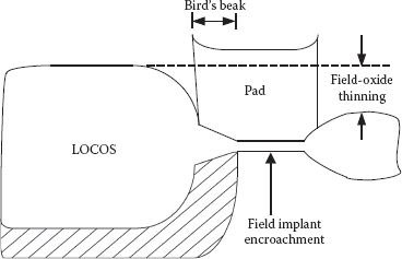
FIGURE 6.7
LOCOS bird’s beak formation, narrow-space oxide thinning, and field implant encroachment. (Redrawn from “Characteristics of CMOS Device Isolation for the ULSI Age,” A. Bryant, W. Häusch and T. Mii, IEDM Tech. Dig., pp. 671–674, 1994.)
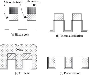
FIGURE 6.8
A typical process flow for shallow trench isolation (STI). (Redrawn from “Characteristics of CMOS Device Isolation for the ULSI Age,” A. Bryant, W. Häusch and T. Mii, IEDM Tech. Dig., pp. 671–674, 1994.)
Another major point of comparison between LOCOS and STI is the ability of reducing junction leakage/improvement in data retention time in gigabit DRAMs. There were two problems in LOCOS: (1) generation of many defects at the edge of volume-expanded field oxide giving rise to leakage current, and (2) high dose of channel implant, which was used to prevent isolation punch-through, increasing the electric field strength across junction. Combination of the mentioned problems enhanced trap-assisted tunneling, hence reduced DRAM cell data retention time [59]. With further scaling down, the problem becomes more acute in LOCOS because thicker field oxide and larger channel stop implantation dose were needed in this process, whereas in STI, depth of the trench is increased which suppresses isolation punch-through even with reduced channel stop implantation dose. Electric field across the junction could be reduced by a factor of three as compared to LOCOS as result of the above at the same density level [60]. This means that STI is much better in terms of reduction of leakage current/enhancement of data retention time.
It is likely that crystal defects might be generated in STI fabrication process of trench etching and densification of filled oxide, which are further aggravated in subsequent processing steps [61]. However, improvements/modifications in processes like round profile of trench, densification at elevated temperature around 1200°C [62] and optimized ion implantations have shown excellent results making STI highly suitable for high density DRAMs. The problem of crystal defects was further attended to at 0.18 μm level through the use of HDP oxide because of its better gap filling property replacing TEOS-O3, which was used at 0.25 μm level [43]. Smaller junction leakage current was obtained in HDP-oxide filled STI than with TEOS-O3 filled STI. With further reduction in device dimensions, better filling of STI gap becomes more important. Bilayers of SOG (silicon-on-glass) and HDP-oxide are used for STI gap filling at 90 nm technology for enhancing the STI properties [48]. Aspect ratio of more than 15 could be obtained for gap-fill compared to less than 4 with HDP. The bi-layer process of SOG and HDP-oxide worked satisfactorily at 70 nm as well [50]. At 60 nm, aspect ratio of isolation trench increased to 7, and the opening became smaller, but SOG and HDP bi-layer process for STI still worked well [52]. CMP planarization is the other key process of STI apart from the oxide filling. The oxide filling topology pattern is not uniform and depends on the comparative areas used by the active region and the field area. However, it is observed that CMP alone is not able to get a flat surface; and combination of RIE and CMP has shown better results [63]. In this process, RIE etch back is stopped before removing all the oxide from the nitride surface, which is then followed by CMP. A proper combination of RIE and CMP eliminates the problem of tolerance accumulation from depositing and etch back of large film thickness.
For monolithically stacked devices, it is critical to use temperature below 400°C for high quality active formation, so as to avoid degradation of Cu interconnects. Hence, to avoid thermal stress problems in Cu interconnects, laser-induced epitaxial growth (LEG) or recrystallization has been used to provide low-temperature isolation technology. Such a scheme is very useful for 3-D integration employing memory layers. A scheme for the purpose has been given for 80-nm DRAM fabrication process [64]. Crystalline quality of LEG was same as that of bulk silicon in terms of its structure and electrical characteristics. It is obvious that such techniques are going to be extremely important for 3-D integration containing memory devices that require back bias applications like DRAM and NAND flash.
6.8 Bit Line, Word Line, and Gate Technology
Sensing signal margin of a DRAM has great impact on cell design which depends on two independent parameters: the storage capacitance CS and the bit line capacitance CB. Realizing a minimum value of CS (~25 fF/cell) at different levels of DRAM density is discussed in Chapter 5, whereas here a brief discussion is added about containing the value of CB. Having smaller CB provides larger sensing signal, which allows faster conversion of sense signal to full data value. As it is in the range of 8 to 10 times CS, CB has to be less than 200 fF–250 fF range for all DRAM density levels. Hence, number of cells connected to a bit lines is typically 256 irrespective of DRAM density. With scaling down the dimensions including reduction in bit line width, bit line capacitance reduces; however, at around 0.15 μm technologies bit line width became smaller than its thickness and fringe capacitance component in CB became a dominant factor. The additional problem of providing lithographic error margin at these reduced sizes was avoided by using SAC etching technology. However, as SAC etching technology uses the different etching rate characteristic of SiO2 and Si3N4, it requires fully encapsulated bit line (and word line) with Si3N4 film. Technology works satisfactorily, but it has the drawback of larger parasitic bit line capacitance due to higher dielectric constant of Si3N4. Parasitic bit line capacitance comprises inter-bit line capacitance and capacitance between bit line with substrate, storage node, word line, and plate node. In addition, interwire capacitance also increased because of reduced distance between bit lines and other conducting layers. Consequently parasitic bit line capacitance does not decrease with further reduction in technology node level beyond 100–150 nm technology unless low permittivity dielectric is used or new cell architecture is employed. Obviously, nonscalable nature of bit line capacitance beyond 100 nm has considerable impact in DRAM chip area especially in terms of number of memory cells connected to the bit while getting satisfactory level of sensing signal. As a small remedy, contact hole etching technology results in considerably reduced parasitic resistance in comparison to SAC hole etching.
Use of hierarchical bit line composed of global and segmented local bit lines has found favor over the conventional nonhierarchical bit line. The global bit line has only inter-bit line capacitance with global bit lines and not with any other conducting lines. Capacitance of local bit lines can be reduced by segmenting the bit lines. Hence, the total capacitance which is the sum of global and local bit lines is considerably reduced [65].
It is important to note that bit line capacitance has a major contributor in terms of junction capacitance, which can be up to 30–50% of the total capacitance value. A major advantage of STI is smaller junction capacitance compared to LOCOS. This reduction is mainly due to the smaller dose of channel stop implantation, and reduction in effective bit line capacitance can be up to 30% more in STI than with LOCOS at supply voltage of 2.0 V. As a result, sensing signal increases from 110 mV in LOCOS to 150 mV in STI at 2.0 V, and the percentage improves with reduction in supply voltage [61]. With the improvement in sensing signal with STI, requirement in storage cell capacitance is relaxed in gigabit DRAMs. Data access time is also improved by nearly 10% because of reduced junction capacitance. However, WSix could be used for bit lines up to only 0.15 μm technology even after improving its sheet resistance. Though having lower sheet resistance, TiSix has not been found effective beyond 100 nm as its sheet resistance also increases with scaling, and it also lacks thermal instability. Hence beyond 100 nm, W and/or some new metal has to be used.
DRAMs become slow because of the RC delay of the word line (and bit lines). The delay is proportional to the square of the length of the word line, which itself multiplies by 1.5 when the DRAM density quadruples. So, the word line delay has been improved by using low-resistance metal silicides like WSix and TiSix for the gate material. At early stage, a sputtered W/Si3N4/poly-Si gate structure and H2O2 selective etching were used to fabricate gate structure, followed by W deposition. Therein, procedural simplification was obtained in a self-aligned W strapped transistor fabrication with a grooved gate structure, and minimization of metal contamination was also achieved using vapor HF selective etching during sidewall spacer fabrication [66]. Sufficiently low sheet resistance of 0.9 Ω/sq. and 1.8 Ω/sq. for NMOS and PMOS, respectively, was obtained for a 0.125 μm wide gate and 0.25 μm wide diffusion. Advantage of using W is that it acts as a better etch stopper than TiSi2 as gate material, having a sheet resistance less than 5 Ω/sq. [67]. However, WSix could be used up to 0.15 μm technology even after improving its sheet resistance through optimization of its composition, morphology, and grain size. The reason behind the limitation is the increase of sheet resistance of metal silicide with decrease in the wire width. Even TiSix having low resistivity found its utility limited to nearly 0.1 μm technology. In each case of Ti and W, a 100 nm doped polysilicon is topped with 100 nm of silicide. With a Ti polycide, a diffusion barrier in the form of 50 Å TiN has to be used between TiSi2 and doped polysilicon.
Limitations of WSix and TiSix meant that different material combinations were to be used for the gate. One such combination was W/WN with low sheet resistance. A W/WN/poly gate was implemented in a 135 nm vertical cell DRAM with planar support transistors. WL with sheet resistance of 7 Ω/sq. was obtained [68]. If WSix gate is used in sub 100 nm design, aspect ratio of the gate stack would become more than 6 so as to keep WL resistance within RC delay limits. Such an aspect ratio creates problems in patterning and gap filling and increases interwire parasitic capacitance (in the same plane). It is observed that the vertical transistor DRAM with use of W/WN gates permits same aspect ratio at 100 nm as at 135 nm node with WSi gates in planar transistor. Hence W technology was extended even for an 80 nm cell transistor with W/WxN metal gate [69], which lowers WL resistance in 176 k cell array by a factor of three with half of the thickness of WSix gate. However, gate stack was carefully optimized using selective oxidation (SO) in order to remove gate etch damage and to cure gate oxynitride. A surface treatment is required before SO to control any abnormal increase in threshold voltage and DIBL characteristics. A 50 nm PVD-W was also used in place of 100 nm CVD-WL to reduce the thickness of the BL to reduce its capacitance without increasing the resistance. Total coupling capacitance was reduced by about 30% in the process. As other alternates Ru and RuO2 metal gates grown by MOCVD (metal-organic CVD) on rf sputtered Ta2O5 gate dielectric have also been used [70]. However, TiN/W metal gate is commonly used for sub-100 nm technology node, avoiding fabrication complexities, even down to 40 nm [71].
For gigabit DRAM, open bit line cell size can be calculated with the help of Table 6.2. The table includes overlay margins up to 0.2 μm for contact holes for different design rules in the range of 0.06 μm to 0.4 μm. It is observed that the requirement of alignment margins becomes so dominant that cell size becomes impractically large simply because scaling down design rules reduces word and bit line pitch, but not the alignment tolerance. A self-aligned contact (SAC) pad formation has to be used for reducing wastage of chip area as well as reducing aspect ratio of the capacitor contact hole [72]. SAC pad anisotropic epitaxial growth avoids the lateral over-growth above the field oxide unlike what is happening with the isotropic epitaxial growth, hence an isotropic epi-growth becomes essential. A comparison between anisotropic and isotropic epitaxial growth and fabrication process of the selective epitaxial contact pad whose top layout view is shown in Figure 6.9 is available in ref. [72].
Si3N4 sidewall spacers of the gate electrode have been formed using SAC technology for a 1 Gbit DRAM [72] while forming SN contact holes (0.16 μm × 0.16 μm). Though the spacers are used to protect the gate material from the contact filling poly-Si due to any process misalignment or etching, a serious problem occurs as spacers cause drain current degradation of the MOSFET. Hence, applying Si3N4 spacers using SAC technology to the word lines (WLs) of DRAM requires caution. A Ge-added vertical epitaxial (GVE) Si pad technology is used to overcome the problem due to the use of Si3N4 spacers as well as the lateral isotropic Si growth in the two-step selective epitaxial Si pad technology [74]. In the given double structure, the first structure is a combination of SA vertical epi pad, a Si3N4 cap on the WL, and a contact plug (CP). As SiO2 can be applied to the sidewalls of the gate electrode spacers, degradation of MOSFET drain current, because of the presence of Si3N4, is almost eliminated. For the second SAC structure, Si3N4 etch stopper on top as well as on the sides of the bit lines can be used without affecting MOSFET. The scheme could provide a 0.23 μm2 folded bit line cell for 0.15 μm technology and alignment margin of more than 0.1 μm.
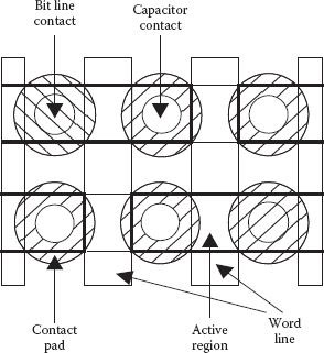
FIGURE 6.9
Schematic top view of an open-bit-line layout of cell with self-aligned contact pads. (Redrawn from H. Hada et al., “A Self-Aligned Contact Technology Using Anisotropic Selective Epitaxial Silicon For Gigabit DRAMs,” IEDM Tech. Dig., pp. 665–668, 1995.)
Other than the alignment tolerance, there is a severe problem of undercutting while vertically etching a thick highly doped polysilicon. A high aspect ratio (AR) of the etching sometimes causes bridge formation between adjacent SNs. A scheme in which buried contact (BC) process is merged with SN makes the SAC process much simpler and makes alignment tolerance free, and removes the problem associated with high AR etching. Such a scheme was successfully used at 0.15 μm on a 4 Gbit DRAM [75].
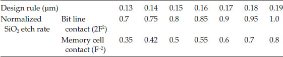
Instead of conventional method of SAC with contact hole printing, a reverse T-shape patterning has been used. The contact area is obtained after SAC etching and then doped poly-Si deposition and poly CMP are used to form memory cell contact pad [43]. AR of the SN contact hole is also reduced by using 100 nm thick W bit line in place of 250 nm W polycide bit line used in 0.18 μm case. Extension of SAC patterning becomes difficult at 0.13 μm technology levels because of the combination of the further reduced size of contact holes and different etching characteristics due to micro loading effect for different contact opening areas as shown in Table 6.3 [45]. To overcome the problem, landing pad technology on bar-type SAC has been developed with which wide process latitude could become available. At 0.13 μm technology level, another problem appeared in the form of the possibility of unwanted connection between BL and SN. Hence, W-BL is fully encapsulated with SiN film to overcome the mentioned problem using SAC process for the self-aligned SN pad. Encapsulation of both, the WL and BL, allows the use of full SAC process for all memory cell contact [45]. Procedure of bar-type SAC patterns for SN pad and encapsulation of BL and WL with Si3N4 was extended at 0.11 μm technology level as well [47].
Normalized SiO2 Etch Rate as Function of Contact Opening Area in SAC Etching
6.10 Interconnection/Metallization Technology
As early as 0.25 μm technology level, constraints of aluminum connecting strips were becoming significant. Electromigration and stress-induced migration started to induce reliability failures in interconnections [76]. Solution was suggested in the form of a TiN/Al-Si-Cu/TiN/Al-Si-Cu/TiN/Ti layered film whose bottom TiN/Ti layer worked as diffusion barrier between the main conducting strip (Al-Si-Cu) and Si substrate, as well as stress buffer at the strip corners [77]. Contact resistance between the TiN and substrate was reduced due to the formation of a titanium layer. Layered conductors along with the sprinkling of other metals with Al improved the situation, but with continued reduction in interconnect pitch with every technology generation, interconnect delay doubled (assuming a constant metal aspect ratio). With an optimum aspect ratio of ~2, deterioration in interconnect RC delay could be restricted to a factor of 1.26, but it was not enough for further generations [78]. Use of suitable low dielectric constant material for inter-strip gap was one option, but use of higher conductivity material like copper was considered better. Along with its low conductivity of 1.7 μΩ-cm (3.0 μΩ-cm for Al-0.5% Cu alloy), Cu had 10 times better electromigration resistance than Al interconnects. However, use of copper posed a few problems like difficulty with plasma etching and hence required damascene structure [79]. Other problems included likely diffusion of Cu through the inter-strip dielectric and difficulty in its adhesion with surroundings, hence needing a barrier layer. Use of Cu and low dielectric technology did improve the performance and reduced error talk and IR drop, but it could work up to 256 Mbit DRAM generations because of the limitations of obtaining fine patterns and the global topology. At gigabit level and beyond, reduced feature size and bigger step height between the cell area and the rest of the region created problems in the form of etching and filling of tiny metal contact holes with high AR. Contact resistance also started increasing due to small area. While investigations focused on the use of Cu and low-k dielectric efficiently, development of triple-level metallization scheme [80] became a very suitable solution in overcoming the depth of focus margin problem for back-end of the line (BEOL) process. In a triple metallization scheme, first metal line was realized in W for local interconnects, and it reduced the level difference between cell array and peripherals considerably, which helped relax design rules for the next two metal lines in Al by more than 50% [67]. W was used as first metal line due to its good contact filling property, and Ti was deposited before the deposition of W to obtain reduced contact resistance. Though contact resistance reduction is not a priority as long as it is only a small percentage of total resistance, filling of contact holes with metals like W or Al requires ohmic and barrier layers between them and the substrate, for the stoppage of metal penetration [61]. Generally Ti/TiN layers are used as ohmic and barriers layers, as Ti forms TiSi2, which works as ohmic layer, and TiN serves as barrier layer. Some of the early applications of triple metallization scheme include a gigabit DRAM [73] and a DRAM at 0.15 μm technology [43].
Considerable research and development concerned the use of copper and low-k dielectric integration at further reduced minimum feature size. Low-k SiOC (k < 3.0) integration was done with Cu at 130 nm node devices and the same technique of manufacturable Cu dual-damascene (DD) interconnect technology was extended to 90 nm node eDRAM devices [81]. Here a maximum of 11 layers, consisting of one local, four intermediate, four semi-global, and two global layers, was used. For local layer, Cu/PE-CVD SiO2 single damascene interconnect line was fabricated which was used for bit line. Though low-k dielectric was not used, interwire capacitance was kept low by thinning the interconnect. For intermediate layers (M2–M5) a stacked PE-CVD SiOC (k <3) film and PE-CVD SiCN (k ~4.9) film was capped with PE-CVD SiO2 film; without SiO2 capping, SiOC structure is damaged during etching and exhibits poor insulating properties. However, SiO2 capping causes resist poisoning problems hence the process requires optimized deposition sequence and use of better resist material. For intermediate layers via-first DD, stacked mask process (S-MAP) technology as described in ref. [81] was developed.
Trench/via-hole DD structures present many problems beyond 100 nm node like poor step coverage of barrier metal/seed Cu, insufficient bottom fill of Cu, and poor mechanical robustness, among others. A hybrid DD structure consisting of PAE (SiLK™; k = 2.65) at wire level, second-generation SiOC (black diamond (BD2)™; k = 2.5) at via level, and SiC (BLOk3™; k = 3.5) as via etching stopper/diffusion barrier [82] was used. It gave a void-less Cu filling and good migration immunity for Cu. Use of Cu continued for 45 nm node having 70 nm wire spacing technology along with the use of porous ultra-low-k NCS (nano-clustering silica) both at wire level and via level. Such a structure was shown to have enough robustness and was called full NCS structure [83]. With full NCS structure and scaling of wire height, capacitance of intermediate-layer wires was not allowed to increase in comparison to the previous generation value of 200 fF/mm at 65 nm node with 100 nm space having NCS/SiOC hybrid structure. Care was taken to completely suppress Cu penetration into NCS, which helped in retaining its TDDB characteristics of earlier generation as well.
With full low-k/Cu interconnects becoming almost universal for high performance, attention focused on the effect of contact resistance in reduced size CMOS devices for further performance enhancement. A direct low-k/Cu DD contact line was used for a 75 nm diameter contact. It was observed that a contact resistance (CT) of 5.4 Ω only could be obtained for the Cu DD contact (Figure 6.10(a)) which was nearly one fourth compared to a conventional W plug (Figure 6.10(b)). The CT reduction ratio increased further with its size reduction as given in Table 6.4 [84].
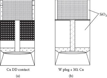
FIGURE 6.10
(a) Low-k/Cu contact, and (b) conventional W plug contact. (Modified from “A New Direct Low-k/Cu Dual Damascene (DD) Contact Lines for Low Loss (LL) CMOS Device Platform,” J. Kawahara et al., Symp. VLSI Tech. Dig. Papers, pp. 106–107, 2008.)
Kelvin Contact to Node Diffusion Resistance as Function of Contact Size
With technology node beyond 45 nm, reliability of Cu/low-k interconnects and inter-metal-dielectric becomes more important. Problems of finer patterning, filling performance, and electromigration of Cu are also to be resolved. Metal doping has been advised to control migration of Cu atoms [85], but it results in higher resistance. CVD Co film has been investigated to replace PVD TaN/Ta in via 1/metal 2 structures for a 32 nm node [86] and has shown good results in terms of filling properties and reliability without affecting wire resistance. Use of CVD Co barrier provided void-free and better Cu migration properties and reduction of nearly 30% thickness of the barrier which provided more space for Cu. Reduction of migration in Cu is because of good adhesion with Co. Even a cursory study of the Cu/low-k interconnect underlines the requirement of continued hard work in the area.
In spite of the acceptance of low-k/Cu interconnect technology, enough reports are not available on its production level adoption for high density DRAMs. At 90 nm design rule capacitor and recessed gate DDR DRAM has been given that successfully integrated low-k and Cu wiring [87]. As the DRAM processes are sensitive to low levels of metal contamination, effect of Cu wiring needed to be studied. In a three-level metallization scheme, generally first level metal (M0) is W and second (M1) and third (M2) levels are Al/Al alloy. In the given scheme, M1, M2, and W via are replaced by Cu and FSG (fluorinated silicate glass, k ~3.5) was used as IMD (intermetal dielectric). Sheet resistance of M1 and via resistance improved by ~45% and ~60%, respectively, compared to Al-based wiring and interwire capacitance decreased by ~50% and ~43% for M1 and M2, respectively. There are additional advantages: a systematic study has also shown no degradation in yield, refresh time, or reliability takes place. Interconnects especially at BEOL at 45 nm or beyond faced additional problems while using Cu. Resistivity of the Cu increases considerably and the necessity of having liner material for preventing diffusion of Cu through the inter-layer dielectric results in reduced available width for Cu conductor [88]. One of the proposed solutions for minimization of increasing resistivity of Cu with decreasing dimensions is to increase the grain size of Cu in narrow connecting lines. However, the procedure is difficult to achieve in practice and a better option is to reduce the thickness of the metal line on Cu using improved sputtering method, ALD, or self-forming barrier layers [89].
Reduced dielectric constant was obtained for inter-level dielectric through doping of SiO2 by fluorine or carbon [90] which formed SiCOH. Nonporous SiCOH is used up to 65 nm level whereas porous SiCOH is used at 45 nm technology node and below. Many design and process modifications became necessary while using SiCOH, especially porous SiCOH, emphasizing the need for alternatives [89]. Air gap technology [90] was again reviewed for the purpose. Although air gap technology requires costly lithography and etching, it provides several advantages over the use of SiCOH in terms of mechanical integrity and thermal conductivity maintenance throughout the die. Hence, air gap technology is also a viable option at a lower technology level of 22 nm or beyond.
6.10.1 Carbon Nanotubes and Graphene Nanoribbon-Based Interconnects
In addition to the aforementioned problems of increasing resistance of Cu at lower dimensions and difficulties faced in employing low-k dielectrics, future scaling is expected to bring more problems for the Cu interconnects including increased current density, which results in reduced electromigration reliability [91]. Hence, efforts are on to find other technologies which could replace Cu interconnects. Promising potential alternatives include graphene nanoribbons (GNRs) and carbon nanotubes (CNTs) [92]. Considerable research has been done to study the applicability of CNTs below the 45 nm technology node as better interconnects [90, 91, 92, 93 and 94].
Despite huge interest in CNT/GNR fabrication technology, their integration into VLSI and especially with semiconductor memories is immature and much more research remains to be done. For example, to replace Cu interconnects, high density and high quality of CNT bundles are desired due to the high resistance of an isolated CNT [95]. Moreover, growth temperature of the CNT interconnect should be kept below 400°C per the requirement of CMOS BEOL process. A CNT via was shown to be integrated in ultra-low-k dielectric (k = 2.6) at a low temperature of 365°C. In fact, most of the work on CNT integration is vertical interconnects or vias because of the tendency of CNT bundle growth perpendicular to the surface [96], whereas long-length horizontal CNT interconnects along with vertical via require challenging steps. Comparatively, fabrication of GNR interconnects in horizontal direction are less challenging than CNTs. Hence, efforts have been made in this direction and in spite of difficulties, carbon films have been fabricated in DRAM trench capacitor using CVD method [97], though not with high electrical conductivity. For improving conductivity of multilayer GNRs, intercalation doping, which was done in bulk graphite, has been suggested [98]. Recently an attempt was made to combine CNTs and GNRs using CVD methods by Fujitsu [99]; however the process needed more work.
Utilization of CNT and CNT bundles as interconnects has many advantages but so far these have not been able to replace Cu mainly because of higher resistance. Methods for reducing CNT interconnect resistance are mentioned as functionalization with accepting molecules, alignment of CNTs within the interconnect, and avoidance of inter-CNT junctions [100]. A minimum sheet resistance of ~55 ohm per square could be obtained with noncovalent functionalization of CNTs. Resistance of aligned CNT interconnects remained constant even with its decreasing width, permitting it be used at lower technology level. Because of the reduced capacitance [101], it was expected that RC delay would be better compared to Cu interconnects beyond 45 nm technology. It was a fair assumption that sheet resistance of CNT interconnects could be reduced to 10Ω per square if all resistance reduction techniques are employed [100].
6.11 Advanced DRAM Technology Developments
As the DRAM density moves into gigabit levels, cell area must be decreased in inverse proportion to the density level increase; otherwise, a larger chip size has to be used. Shrinking of feature size is the main option for decreasing the cell area, but it invites a host of new problems whose solutions must be available. As the minimum feature size (F) is not reduced by the same factor as the DRAM density increases, it means chip size has to be increased, and, in combination with the reduction in feature size it shall result in yield loss, unless remedial measures are taken in terms of circuit innovations and technological advancements. As observed from Sections 6.1 to 6.9, which noted an important feature of DRAM technologies that transitions are smooth and some form of continuity is maintained even when other new processes/steps are taken. To explore the advanced DRAM technology developments, the spectrum is divided in four sections, of which three sections contain technology node descriptions of stacked technology. This bifurcation is not only to facilitate understanding but to expound upon the different features, in spite of the conventional continuity. The final section discusses deep trench technology beyond 100 nm level.
6.11.1 0.18 μm to 0.11 μm DRAM Technology Development
Capacitance density, defined as the cell capacitance divided by the projected area of the storage node has to be increased. For a consistently maintained value of 25 fF cell capacitance, a capacitance density of 145 and 330 fF/μm2 is required for the 1 and 4 Gbit DRAMs, respectively. Hence, storage capacitor technology becomes very important. Refinements in the usage of Ta2O5 as capacitance dielectric, and the development of Al2O3 capacitors have been reported extensively for and below 1 Gbit DRAM density. With reduced feature size, and continual reduction in supply voltage/cell array voltage, charge stored in the cell capacitor becomes small, affecting the data retention time. High resolution lithography becomes a must along with suitable etching processes at this range of technology-nodes especially for the patterning of critical layers like active region, gate, and bit lines. At 0.18 μm and lower level feature size one of the additional critical factors is the variation in threshold voltage of cell transistor which greatly affects the functionality and data retention time. KrF lithography has been used in 0.18 μm to 0.13 μm technology range, mainly to save investments in a new kind of lithography. Resolution enhancement and proximity effects suppression are therefore used to decrease critical dimension variation to less than 25 nm across the 6-inch mask.
Bit line contact and storage contact hole sizes also become small with decreasing feature size and high overlay accuracy is required. Selective etching between silicon oxide and nitride has been used for making SAC to overcome the mentioned problem. For 0.20 μm design rule, SAC process has been used to get overlay accuracy within 50 nm with Si3N4 spacer between the gate material and the contact filling polysilicon [73]. Since silicon nitride spacers cause lowering of MOSFET current [105], silicon nitride SAC technology was not desirable for word lines of DRAM. Hence a two-step selective epitaxial Si pad has also been used which is a combination of perpendicular anisotropic and lateral isotropic silicon growth [72]. However, as the lateral expansion controllability was not satisfactory, Ge-added vertical epitaxial Si pad technology has been used for gigabit DRAMs at 0.15 μm design rules [74].
Probably first fully working 1 Gbit SDRAM fabricated in 0.18 μm CMOS technology was devised by K.N. Kim and others in 1997, overcoming major limitations at this small feature size and comparatively large size chip [106]. Critical dimension variations were improved to less than 30 nm for average critical dimensions of 220 nm by using a high-resolution technique of OPC and elimination of standing wave effect using antireflection layer. More than 25 fF/cell capacitance was obtained in a one cylinder stacked structure with hemispherical grains and Ta2O5 as capacitance dielectric. Another gigabit DRAM fabricated in 0.18 μm technology overcame the problems related with photolithography by employing straight line and space patterns, a fully planarized surface, and alternating PSM along with SAC technology [107]. CMP was used to completely planarize the wafer before each photolithographic step like poly-plug patterning, bit line, and first metal layer patterning. While having full planarization, deep and higher aspect ratio contact holes need to be realized, which was successfully done using dual frequency RIE equipment without hard mask. Being fully planarized, stacked capacitor necessitates capacitor height to be small for reducing aspect ratio of metal 1 contact; hence Ta2O5 film dielectric having oxide equivalent thickness of ~2.9 nm capacitor was used. To get 25 fF/cell, capacitor height was nearly 0.9 μm.
DRAMs based on 0.15 μm technology got greater attention as a transitory technology between 0.18 μm and 0.13 μm technology mainly on account of usage of both KrF and ArF lithography, respectively, and the increase of wafer thickness from 200 nm to 300 nm. Key technologies at 15 nm level were lithography, oxide filling in STI, polycided gate, self-aligned memory contact pad, and Ta2O5-based cell capacitor. Economic factors were responsible for the continued used of 248 nm KrF lithography at 0.15 μm technology level, though resolution enhancement and proximity effect suppression continued. Mask error amplification was also suppressed and this combination of improvements in lithographic process resulted in less than 25 nm variations in critical dimensions on a 6-inch mask [43]. At 0.18 μm technology O3-TEOS oxide filling was used in the STI process. However, at 0.15 μm node and beyond, oxide filling without voids was done using high-density plasma (HDP) oxide, resulting in lower junction leakage current than those of O3-TEOS-filled STI.
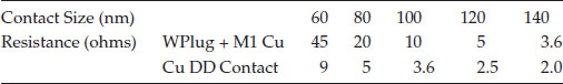
Consistent decrease in the minimum feature size is one of the basic reasons for increasing DRAM density. However, the same rate of decrease could not be followed in terms of the alignment tolerance between contact holes and word lines or bit lines. Therefore, SAC structures were used and for 1 Gbit DRAM Si3N4 spacers have been used. However, presence of spacers affects drivability of transistors, hence a better option was suggested in ref. [74] in which double SAC cell in combination with a Ge-added vertical epitaxial (GVE) Si pad technology was used. First SAC structure is a combination of self-aligned vertical epitaxial pad, a Si3N4 cap on word line, and a contact plug. The second SAC structure is conventional using Si3N4 stoppers on the top as well as on sides of the bit lines. This double SAC scheme reduced the cell area from 0.39 μm2 to 0.23 μm2 in 0.15 μm technology with 0.1 μm alignment tolerance as shown in Figure 6.11. For 1 Gbit DRAM estimated alignment tolerance for an 8 F2 folded bit line cell in 0.2 μm technology node is hardly 0.01 μm for a conventional pad, which improves to nearly 0.08 μm for an epitaxial pad and further increases to 0.14 μm in a GVE pad + Si3N4 cap. However, 4 Gbit DRAM with 0.15 μm technology node is practically not possible with a conventional pad because of the non-availability of any tolerance, whereas its corresponding tolerances are 0.06 μm and 0.09 μm, respectively, with epi pad and GVE pad + Si3N4 cap.
FIGURE 6.11
Memory cell layouts of 8 F2 folded bit-line arrangement using 0.15 mm design rule with 0.1 mm alignment tolerance. The cell area is reduced from 0.39 mm2 by new SAC technology using GVE Si pad with Si3N4 cap structure in place of former epi pad SAC technologies. (Redrawn from “A 0.23 μm2 Double Self-Aligned Contact Cell for Gigabit DRAMs With a Ge-Added Vertical Epitaxial Si Pad,” H. Koga et al., IEDM Tech. Dig., pp. 589–592, 1996.)
Trench DRAM technology has also been shown to be very effective at 0.15 μm design rules [108] by improving the important parameters like cell capacitance and performance and reducing resistance and device leakage. Using isotropic silicon etching, enlargement of the bottom part technique is applied to increase the capacitance from 22 fF to 33 fF/cell. The resistance between the trench and the active area is decreased by using a self-aligned oxide hard mask STI process from 11 kΩ to 4.5 kΩ.
At 0.13 μm level most of the key technologies remained in use that were used at 0.15 μm or 0.18 μm level, for example, Ta2O5 MIS capacitor, self-aligned landing pads, low resistance word line and bit lines, and triple metallization. However, these high temperature processes make them suitable for stand-alone DRAMs but not for embedded DRAMs and require suitable modifications. In addition, a significant problem arises that the SAC process which was applied to form self-aligned landing pads around word lines could not be adopted due to the reduced process margin of SAC etching [45]. Around 0.13 μm technology and beyond, both word lines and bit lines need to be encapsulated with Si N film, which would allow full SAC process so that the possibility of shorting bit line to storage node is eliminated and all memory cell contacts with bit lines and word lines are formed in self-aligned form. A polyamorphous one-cylindrical capacitor (PAOCS) was realized in which capacitance was increased by using both inside and outside of the storage cylinder as capacitor plate. The outside of the storage capacitor cylinder was formed by polysilicon at less than 450°C whereas the inside was formed by amorphous polysilicon with hemispherical grain, and Al2O3 as dielectric which did not require high temperature annealing of Ta2O5. Low temperature process was suitable for embedded DRAM application, and it also aided in reducing the resistance of W bit line contact resistance. Smaller height PAOCS capacitor helped in getting the aspect ratio of metal contact within a limit of 0.1 μm with the use of full CMP, and so the KrF lithography could be extended to 0.13 μm nodes. Developed 1 Gbit DRAM cell size was approximately 0.13 μm2 and the chip size nearly 267 mm2.
Word line and bit lines encapsulated by Si3N4 for pad separation with CMP process, all pads formed by line type SAC, and low thermal budget Al2O3 dielectric PAOCS capacitors were some of the key technologies used at 0.13 μm level and were again used at 0.11 μm technology for the realization of a 4 Gbit DRAM, along with the continuance of KrF lithography [46,47]. Hard OAI was used in the KrF lithography for resolution enhancement and newly developed scattering bar OPC pattern was used to improve DOF margin. An important problem to be tackled at 0.11 μm level is the inter-layer dielectric gap filling having as high an aspect ratio as 10 or more. SOG was used for this purpose and after annealing it gave very satisfactory results. Metal contact which landed at bit lines reduced very high aspect ratio in conventional scheme to manageable limits and then metal contacts were formed with a borderless contact process available in ref. [46]. Some of the key technologies used at 0.11 μm technology are given in Table 6.5.
A Few Key Process Features of 4 Gbit DRAM at 0.11 μm Level
Lithography |
KrF |
High NA, OAI and OPC |
Isolation |
STI |
HDF gap fill |
Transistor |
GNOx |
4 nm |
WL |
T Six |
|
Cell structure (size .225 μm × .465 μm) |
Stack pads, and pads for cell contact, storage nodes |
Line-type SAC and CMP separation |
Storage |
Inner HSG scheme |
PAOCS + HSG |
Capacitance dielectric |
toxeq 30 angstroms (Å) |
Al2O3 (40 Å) |
Metals |
Triple metal |
CVD Al |
6.11.2 100 nm to 50 nm DRAM Technology Development
As design rule of DRAM fabrication goes below 100 nm some new process integration technologies have been utilized along with the few technologies used in the 0.13 μm to 0.18 μm era. For DRAM cell performance improvement beyond 100 nm, parasitic resistances and capacitance in the cell structure were necessary to be reduced; otherwise, they would have offset the advantages of the shrinkage technology [109]. New technologies like spin-on-glass (SOG) became essential for oxide gap-filling for STI and ILD processes [48]. Dual gate of CMOS process was adopted in low voltage DRAMs because low threshold voltage PMOS could be made using conventional method of buried contact [110]. Recessed channel-array transistor (RCAT) [23] was now used to overcome the problem of short channel effect. Deep trench (DT) technology with checkerboard cell layout process enhancement was also employed successfully at 70 nm scale [111].
Below 100 nm, DRAM performance of multi-gigabit density is seriously affected by the memory cell characteristics and parasitic resistance and capacitance of the transistor channel, and bit lines and node resistance must be decreased as well. To reduce the parasitic resistance, the memory cell is realized having poly Si/WxN/W gate, source/drain junction with Co siliciding, and CVD-W cell pad and bit line contact. Though Co saliciding on cell area increases junction leakage current [112], the limitation is overcome by using elevated source/drain selective epitaxial growth using UHV-CVD at 700°C to avoid direct formation of Co silicide on cell as well as core and peripheral region [109].
Other problems below 110 nm design rules include formation of voids while filling in STI with high-density plasma (HDP) scheme. Mechanical stress is also increased between HDP oxide and silicon due to their different thermal coefficients of expansion [113]. Moreover, in conventional STI, higher doping concentration of the channel stop increases GIDL current and deteriorates hot carrier immunity of DRAMs. To overcome these problems void-free STI was developed using polysilazane-based inorganic spin-on-glass (P-SOG). It showed void-free gap filling and lower compressive stress than HDP oxide and hence held promise for further lower feature size fabrications. As parasitic bit line capacitance is partially due to the use of Si3N4 bit line spacers, a top spacer storage node contact (TSC) has been developed, process flow of which is available in [49].
Use of TSC process reduces the loading capacitance by removing the additional capacitor landing pad layer that was used earlier in diamond-shaped OCS, and it also allows easy gap filling with ILD oxide. In addition, it also increases the breakdown voltage, due to lower plasma damage during TSC formation.
A highly manufacturable 90 nm DRAM technology was developed in 2002 using ArF/KrF lithography and some novel integration schemes [48] like spin coating oxide for STI and ILD processes, and diamond-shaped storage node for large capacitor area having better mechanical stability. Dual-gate oxide scheme was also used in the DRAM development for memory cell transistor and the transistors used for peripheral circuit with an objective of keeping the off current below 0.1 fA/cell. Critical patterns, such as active and gate layers, SAC pad, bit line, BC, and storage node contact, could get more than 0.3 μm DOF margin with the use of ArF lithography and hard mask etching. SOG and HDP oxide layers were used for STI gap filling and only SOG oxide filling was used for interlayer dielectric gaps. A comparison between the cell layout of a conventional OCS and newly developed OCS showed that the use of diamond-shaped structure eliminates the criticality of the layout of conventional storage node, which allowed the use of KrF lithography for it even at 90 nm technology. Mechanical stability of this structure is also better. In essence, diamond-shaped OCS provided more freedom for lithography, larger capacitance, and better mechanical stability. A MIS capacitor with AIO/HFO dielectric [114] with equivalent oxide thickness of 25 Å was used which provided 23 fF/cell capacitance.
DRAM with 80 nm technology was developed for the first time in 2003 using ArF lithography, recess channel array transistor (RCAT), low-temperature MIS capacitor, and TSC. ArF lithography is used in fabricating RCAT, which shows a distinct improvement in the performance of RCAT over planar transistor in terms of distribution of threshold voltage and the distribution of the DIBL and junction leakage current. The TSC continued to provide advantages like easy gap filling with ILD oxide, reduction in the bit line loading capacitance and higher breakdown voltage. In addition, another important feature was that the landing pad that was used in 90 nm technology [48] could be eliminated and it saved expensive ArF lithography. To obtain cell capacitance of more than 25 fF, a low-temperature MIS structure (polysilicon SN, Al2O3- HfO2 film dielectric, TiN top electrode and W plate node) was realized in a low thermal budget of <500°C. Another manufacturable 6 F2 DRAM technology at 78 nm design rule was given by Micron Technology Inc. using MIM capacitor with composite high-k Al2O3/HfO2 dielectric with TiN as electrode [115], which occupied only 0.036 μm2/cell. For DDR2 DRAM design, boosted word line voltage of more than 2.5 V was used with a supply voltage of 1.5 V. Hence dual-gate oxide was used with array oxide being 5.5 nm thick and peripheral CMOS with 3 nm thick oxide. Parasitic activity and noise were reduced by using WLs and BLs covered with tungsten.
A number of DRAMs were reported at 70 nm technology level either using MIM capacitors [50,52,116], with minor variations, by adopting better part of the technologies of the previous generation for continuation sake. Technologies employed at 70 nm as well as 90 nm level which illustrate a good measure of continuity and changes in the technology are available [50]. Instead of KrF lithography, ArF lithography with simple layouts having straight lines and resolution enhancement techniques was used to get more than 0.3 μm of DOF margin for critical layers. To increase the mechanical stability of the diamond-shaped OCS, the bottom part was buried in molded oxide. The structure was further improved at manufacturable level for DDR-3 applications [116]. Important changes in the technology were made in a report given by C. Cho and others with 68 nm design rules to obtain a cell size of 0.028 μm2 (6 F2) and employed sphere-shaped RCAT (S-RCAT) [24] and double exposure technology (DET) for better resolution [52]. Figure 6.12 shows the layout with word lines and bit line having 2F and 3F pitches. As the word line was made of tungsten and its length was 3F, its resistance was decreased by nearly 25%, and bit line capacitance was decreased by nearly 50% (50 fF/line with 256 cells) compared to an 8 F2 cell. Thickness-optimized multilayer HfO-AIO dielectric was used on TiN metal electrode [117] to realize a 65 nm technology DRAM unaffected by post-thermal process. Cell capacitance of 25 fF was obtained while using equivalent oxide thickness of 11 Å, and leakage current was less than 1 fA/cell. This multilayer MIM capacitor with the dielectric used was claimed to be practicable beyond 50 nm technology.
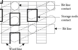
FIGURE 6.12
Part of the cell layout of a 6 F2 DRAM. (Modified from “Integerated Device and Process Technology for Sub-70 nm Low Power DRAM,” C. Cho et al., VLSI Techn. Dig. Tech. Papers, pp. 32–33, 2004.)
Further reduction in feature size was reported in the form of a 6 F2, 1 Gbit DRAM at 56 nm technology having a cell size of 0.019 μm2, which was the smallest device with a fine performance level as well. Technologies used at 70 nm now needed more advancement especially for critical patterns, isolation, and inter-layer gap fill. A comparative statement is available for the technologies used at 56 nm level with the technologies used in the previous generations [53]. At 80 nm and 68 nm, HDP was used for isolation which is supplemented with spin-on glass (SOG) at 56 nm, whereas the corresponding metallization changed from triple level to quadruple level. Storage node is realized in metal for 56 nm in place of TSC or contact type poly-Si of the previous generations. Capacitance form changed from AHO (MIS) to HAH (MIM) and then to ZAZ (MIM) at 56 nm with SN without landing pad.
For critical layers, ArF immersion lithography was used which provided photo lithographic process margin with DOF more than 0.1 μm. Dual poly gate (n+/p+) with selective epitaxial layer were used for the elevated source drain. SRCAT was continued to be used, however for increasing cell transistor current, localized asymmetric channel (L-ASC) doping in which no channel doping is done at storage node [118] was developed. Simulated 2-D junction profiles of the different cases have been shown in ref. [53]. Junction leakage current reduced up to one-third and the body effect also improved by ~6% with L-ASC. One major difference over earlier DRAMs was the use of ZrO/AlO/ZrO (ZAZ) dielectric with EOT of 75 Å for the MIM memory cell, which provided cell capacitance of 25 fF with leakage still less than 1 fA/cell.
6.11.3 Sub-50 nm DRAM Technology Development
In two fine reports in 2005 and 2006, Kinam Kim has outlined major problems that needed to be addressed for DRAMs at 50 nm and beyond [119,120]. Shrink technology, which was the most important factor in ever-increasing density of DRAMs, brought with it a few new issues as well. Process windows became smaller and variations in parameters due to process uncertainties increased further. Many problems which have been outlined in earlier sections like requiring sufficient cell capacitance in decreasing projected area, leakage of current from storage node junction, short channel effect in devices, degradation of retention time, reduction in transistor driving current, became more acute now. Along with improved lithography and etching techniques, new dielectric materials having compatibility with storage electrode were needed. Requirement of new device structures with novel approaches also became indispensable in order to keep pace with required Ion and controlled Ioff.
MIM structures with high-k dielectrics and metal electrodes have been used in sub-100 nm DRAMs to provide a minimum of 25 fF/cell. Development came in the form of the type of dielectric and the metal used for electrode. Around 60 nm ZrO was preferred whereas for 50 nm design rules STO or BST with TiN electrode was used. However beyond 50 nm, in place of TiN electrode, Ru metal is preferred which ensures high value of dielectric constant. Efforts continue to somehow increase the capacitor area/capacitor density without affecting its projected area.
To obtain the consistent value of 25 fF/cell capacitance for DRAMs at 45 nm, device needs a thin layer of oxide equivalent in the range of 6–7 Å [121]. Dielectric material layer like HfO2/Al2O3 stack and HfxAlyOz used up to around 70 nm, but were not able to satisfy the conditions needed at 45 nm [117]. Even the ZrO2 film formed using atomic layer deposition (ALD) at 50 nm scale could not be used satisfactorily on account of negative biased leakage current [121]. New material like Ru has also been used for electrodes, but while the process was still to mature, dielectric film structures from ZrO2 and Al2O3 have been shown to work even for mass production at 44 nm scale [54] as its equivalent oxide thickness was lowered to 6.2 Å with TiN electrode.
The problem of short channel effect which leads to enhancement of electric field at junction nodes degrades the retention time. Severity of the problem was greatly minimized through the use of RCAT and SRCAT [23,24] in which effective gate length was increased. However, beyond 50 nm other alternatives were needed for getting good performance from a cell transistor. Body tied FinFET is one such alternative which provides good progress toward short channel effect and provides excellent sub-threshold swing [122].
FinFET technology was expected to give quite satisfactory performance down to 30 nm node, along with the use of some other transistor structures like vertical pillar [123] and saddle fin [124]. However, beyond that, vertical transistors with SGT or S-SGT (slacked surround gate transistors) [2,3] are to be used.
Fully integrated, 8 F2, 1 GB DRAM with smallest cell size of 0.15 μm2 [54] was created by Hynix Semiconductor. Key process technologies used were ArF immersion lithography, peripheral transistor with WN barrier metal, and tungsten on n+ poly-Si. Cylinder-like storage node with ZAZ dielectric (ZrO2/Al2O3/ZrO2) and triple-metal layer including copper were also used. To overcome the problem of nonscalability of the gate oxide thickness in line with the overall reduction in feature size at this level, saddle fin cell transistor which has the added advantage of improving short channel effect, including DIBL (drain-induced barrier lowering) and sub-threshold swing to 6 mV and 85 mV/dec was used.
With the DRAM working voltage coming down to 2 V and 1.0 V, new technologies are to be adopted. Signal margin which is further reduced due to the reduced array voltage, has to be maintained at a level that is easily picked by the sensing scheme. A buried word line (bWL) scheme has been introduced for a 6 F2 46 nm DRAM that overcomes the problem through (including) reducing the bit line capacitance, which has size of 0.013 μm2 and uses a three-dimensional EUD (extended u-shape device) array device structure [71] with a gate oxide thickness of 4 nm and a TiN/W metal gate. In fact TiN/W buried WL which is fabricated below the Si surface not only forms local interconnect but metal gate as well. In the proposed structure one bit line contact is shared by two cells, reducing chip area, and the buried WL isolates two adjacent capacitor node junctions. Simulations have shown that in the bWL structure bit-line capacitance is halved and word line capacitance became one-third that of a conventional structure. As a result, cell access time became shorter, power consumption was reduced, and the signal margin improved.
6.11.4 Sub-100 nm Trench DRAM Technology Development
As the DRAM cell minimum feature size goes below 100 nm range, short channel effect creates more and more problems. One known and workable solution was to increase substrate doping but, the remedy itself creates another problem in the form of increasing electric field [23,125]. Alternate solutions included vertical access transistors in deep trench technology [28,125] or recessed devices in stack capacitor technology [23,49]. Basically, the array transistor channel length was extended in these schemes, which avoided substrate doping increment with its resultant positive effect. However, it decreased the drive current of the array transistor and also decreased its Ion/Ioff ratio; hence, the effort was to overcome this important limitation.
A planar DRAM cell device with a novel checkerboard cell layout has been reported and its integration at 70 nm level was achieved basically on highly asymmetric, inhomogeneous doping profiles along the channels [111]. Basics of the checkerboard (CKB) layout are shown in Figure 6.13. High symmetry in deep trench (DT) and in active area (AA) with equal lines and spaces overcomes the scalability problem faced earlier in the MINT layout [27] due to DT-DT spacing and overlaps between AA and DT. Since due to high selectivity of Si <100> to Si <110> 45° rotated substrate was used as shown in Figure 6.13; it increased capacitance by more than 25%. Hemispherical grains and the use of Al2O3 ALD, a high-k dielectric used first time in DT process, also increased the capacitance. However, to reduce the parasitic bit line contact to word line capacitance, oxide spacers provided good results instead of nitride spacers. A significant advantage of this technique was the objective of extending the planar DRAM cell channel length, which was achieved without compromising with the device drive current. Another DRAM cell at 70 nm generation employing CKB deep trench technology was given by C.H. Chung and others [126]. In this DRAM cell, designed buried strap was in opposite direction of each adjacent row of deep trench. Fabricated cell showed excellent refresh characteristics. Dual gate spacer technique—that is, different gate spacer thickness between cell array and core/periphery—is used to achieve the dual objective of suppressing periphery device short channel effect and ensuring sufficient process window for the array devices.
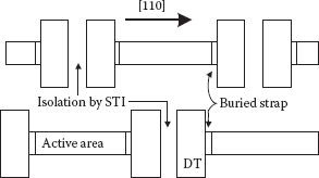
FIGURE 6.13
Schematic of MINT layout with substrate orientation. (Redrawn from “A Highly Manufacturable Deep Trench Based DRAM Cell Layout with a Planar Array Device in a 70 nm Technology,” J. Amon et al., IEDM Tech. Dig., pp. 73–76, 2004.)
In a possible roadmap for the DRAM products, it was predicted that by the year 2010 data rate would be around 6400+ Mbit per second for DDR5 systems and supply voltage and the array voltage would have to be decreased to 1.2 V and 1.0 V, respectively, to achieve array timing of 8 ns [126]. With the expected reduced external supply voltage and the array voltage, if the storage cell capacitance is to remain nearly constant at 30 fF, bit line capacitance has to be decreased to 40 fF and 35 fF to get a cell signal of over 150 mV at 50 nm and 40 nm technology level, respectively. It may be noted that these calculations were based on the DRAM employing a trench cell array with 256 cells per twisted, folded, bit line array. To achieve mentioned shorter array timing of 8 ns and sense signal of over 150 mV at array voltage of 1.0 V (50 nm node) or 0.9 V (40 nm node), the trench resistance and the capacitance dielectric equivalent oxide thickness of the capacitor dielectric must be reduced. A hemispherical grain MIS capacitor having Al2O3 as dielectric (CET = 3.5 nm) and low resistance TiN liner connection of top metal capacitor plate to the poly-Si buried strap which connects to the cell transistor, reduces trench resistance by half. It results in the reduction of array timing by 1.5 ns enabling to reach the goal predicted by the DRAM product road map. For the 50 nm technology, a MIS capacitor in trench (TiN/HfSiON) has also been developed with CET = 2.5 nm [127].
To keep level of array transistor Ioff less than standard 1 fA/cell is a huge challenge especially for technology node beyond 100 nm. Trap-assisted tunneling leakage starts taking place because of increased electrical field at any higher doping concentration area, even if localized. For a planar array device, trench DRAM was successfully scaled down by Amon and others [108] at 70 nm and RCAT [23] at 80 nm. A new structure on the lines of RCAT have been given which forms an extended U-shaped device (EUD), which meets the requirements of Ioff and Ion at 60 nm node and also improved sub-threshold slope to 97 mV/dec [126]. Local damascene FinFET structure has also been developed for trench DRAM, as shown in Figure 6.14 and at 90 nm technology sub-threshold slope (SS) reduces to 77 mV/dec with Ion = 40 μA; for 40 nm case, predicted values were, SS = 89 mV/dec, Ioff < 1 fA, Ion = 40 μA [128].
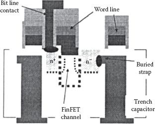
FIGURE 6.14
FinFET in trench cell integration scheme. (“Trench DRAM Technologies for the 50 nm Node and Beyond,” W. Mueller et al., Int. Symp. on VLSI Tech. Sys. and Appli., pp. 1–2, 2006.)
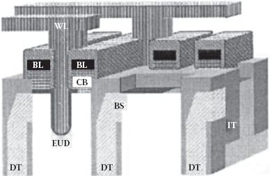
FIGURE 6.15
Schematic 3-D view of a novel word line over bit line cell. (“A Novel Cell Arrangement Enabling Trench DRAM Scaling to 40 nm and Beyond,” L. Heineck et al., IEDM Tech. Dig., pp. 31–32, 2007.)
As also indicated earlier, DRAM needs to support/interface with high data rate at reduced external voltage. Schematic of a new cell arrangement called word line over bit line is shown in Figure 6.15, where the total bit line capacitance is reduced by nearly 30% [129]. It results in a faster cell access. In this scheme the most important innovation is that word line is realized in the first local interconnect metal layer, and the bit line is formed before the formation of array device and word line. It is also possible to realize the word line with very low resistance without affecting any other fabrication step adversely. A DRAM product at 48 nm was successfully obtained confirming the performance and shown to be scalable to 40 nm levels, which used some of the following advanced features used earlier as well. The checkerboard trench cell [111] and immersion lithography [55] helped avoidance of double patterning [52]. In addition, the EUD array device [127] helped in reducing leakage and hence satisfying data retention requirements.
Continued scaling, advancements in DRAM technology, and circuit innovations have made stand-alone DRAM the cheapest memory. However, DRAM’s data transfer with various other digital functions created bottlenecks especially in the manufacturing domain, like input/output devices, increase in the number of pins, and so on. Around 1997, efforts started to utilize the low cost of DRAM in increasing the performance of digital function by combining the memory and logic on the same chip. Soon it was observed that further scaling was heading fast toward fabrication of complete system-on-chip (SOC) devices. Typical SOCs could contain random logic, intellectual property (IP) blocks like dedicated processors and controllers, register files, and analog components such as PLLs and D/A (A/D) converters [130].
Realization of SOC not only improved system performance, it opened possibilities of new applications because of a number of advantages. Important among these are (1) high bandwidth operation between DRAM and logic, (2) lower power dissipation, and (3) overall reduced size (hence cost) of the chip. High-speed on-chip logic in embedded DRAM reduces latency, which is much less than that of off-chip DRAM [131]. In comparison to embedded SRAM, capacity of embedded DRAM is nearly four to five times higher, although it requires special processing steps, which is not so with SRAM. Additionally, embedded DRAMs (eDRAM) consume only 30% of the SRAM power in standby mode and 10% in active mode for a general-purpose process [131], mainly because of fewer transistors per bit used. Embedded DRAM is superior in terms of soft-error-rate (SER) as well because of its larger value storage capacitor. By having DRAM and the logic on the same chip, high power consumed by the I/O modules is also avoided.
Promise of high performance has given great boost to the realization of SOCs, as SOC, which embeds DRAM array to logic, is found to be the best solution where large amounts of data are to be communicated at high speed—for example, a graphics accelerator of video games and fast Ethernet router [132]. However, merging of the DRAM and the logic requires reducing differences in manufacturing process. For an SOC, compatibility of design rule and IP module library between embedded DRAM and logic is essential [131]. Process of reconciling compatibility for the embedded DRAM and logic is now mainly dependent on two different approaches: (1) memory circuit is incorporated in a high performance technology optimized logic, or (2) the logic circuit is incorporated in a technology-optimized high density low-performance DRAM. Obviously both the options have their advantages and limitations. When option (1) is selected additional steps are required to fabricate dense DRAM array and precautionary steps are also needed such as with deep trench (if TCC is used) dual gate oxide, and silicidation is not to be used on drain/source region. In this technology option logic circuit is not affected but the DRAM cell size becomes nearly double as SA bit contacts are now restricted. Size affects the density and architectural advantage of the commodity DRAMs.
If option (2) is selected, technology is to be tailored to improve the logic circuit/peripheral transistor performance and for the additional interconnect layers. It requires additional processing deployment of dual gate oxide which helps in optimizing transistor fabrications in DRAM cell wing I/O transistors with thicker gate oxide and random logic transistor with thinner gate oxide (with lesser gate voltage). Dual threshold voltage increases fabrication complexity but reduces leakage in DRAM cell and retains better performance in logic circuit. It is observed that process complexity of option (2) is about 15% less than option (1) [130], but the logic performance deteriorates 20 to 35%. In general, if a function needs memory exceeding 50% of the chip area, DRAM-based technology is preferred. It is important to note that minor intermediate process steps in the two options do vary with changing technology level and also depend on whether the DRAM cell uses TCC or SCC of COB or CUB type.
Huge advantages of merging the DRAM and logic on the same chip, however, do not come easy and the integration is challenging. Trade-offs are required in terms of performance/power/chip area, and depending on the variables involved, processing steps are differently selected. Since logic process and DRAM process are not compatible on many counts, options are invoked. An optimum eDRAM should combine the most advanced cell array, with minimum size and power consumption, with high performance logic at the least possible manufacturing cost. However, the process requirements of high-performance logic and the advanced DRAM are partly contradictory. Following are among the main issues in DRAM technologies compared with logic technologies:
1. Trench capacitor cell or stacked capacitor cell—High-density DRAM cells can be realized using trench capacitor cell (TCC) or stacked capacitor cell (SCC) but process steps should not be mixed with the logic realization. For examples in TCC, capacitance is formed before gate oxidation; hence, thermal process steps are not needed after the transistor module fabrication. As a result logic devices do not degrade in TCCs. However, with SCC few high temperature processes are used like storage node insulator formation, SiN deposition for SAC, and it is always desirable to optimize these thermal operations in order to reduce their damaging effects on transistors; silicide process for the source/drain also is affected by high temperatures. Another advantage with TCC is that because of its flat topology, there is no difference between DRAM cell level and logic regions which results in having contact holes with low aspect ratio. Interconnection layers are, therefore, easier to fabricate, whereas inherent high aspect ratio creates lithography restrictions and comparatively difficult metallization in SCC.
2. Transistors in DRAM cell and logic—As requirements from the transistors are different in a stand-alone DRAM cell and for a random logic, these are fabricated differently. Some of the important features are shown in Table 6.6. Consequently in eDRAM, trade-offs are used and generally a middle of the path combination of processes is used depending on the technology used.
3. Levels of interconnects—In DRAMs, the architecture requires only two layers of metal where the second layer is generally laid with relaxed pitch; hence, metallization is rather a simple process. In the general logic, interconnect has now become very specialized with six or more layers for local, semi global, and global needs. Along with aluminum, copper with low dielectric material high aspect ratio contacts have become essential.
Comparison of Fabrication Approach in Conventional DRAM and Logic Transistors
Parameter |
DRAM |
Logic |
Threshold voltage, Vth |
Higher value to reduce leakage current and off current |
Comparatively lower value to improve performance (with > Ion) |
Transistor gate voltagea |
Enhanced value to improve performance, Vcc = 2.5 V |
No enhancement, Vcc = 1.5 V |
Gate oxide thicknessa |
Thicker gate oxide to prevent punch-through with increased gate voltage, e.g., 60 Å |
No increment in gate oxide thickness, e.g., 30 Å |
Silicidation of drain/source |
Not used, affected at higher temperature |
Silicidation is used to reduce drain/source resistance |
Self-aligned bit contact |
SAC is used to connect bit line to the cell transistor |
Not used |
Gate encapsulation to avoid shorting with gatea |
Isolation techniques are used; gate length = 0.23 μm |
Minimum gate dimensions are used which prevents use of SA contacts, gate length = 0.14 μm |
Gate material |
Single work-function (usually n-type) gate material is used to reduce cost |
Dual work-function gates are used for better performance |
a Numerical values of the parameters are for 0.18 μm embedded DRAM technology.
Trench cell technology was preferred for reasons mentioned above at 0.5 μm, 0.35 μm, and 0.25 μm technology levels in which commodity DRAM process was used up to trench isolation. The source/drain of the MOSFETs was silicided and W bit line and first level Al were formed using DRAM process [133,134]. A silicided-bridged substrate-plate trench (SPT) capacitor DRAM cell was fabricated using double-sacrificial-Si3N4-sidewall (DSS) process and silicidation at 0.25 μm design rule [135]. A closed ring of deep trench isolation (DTI) is deployed around every n-well in the logic parts, which helped in reducing chip size up to 30% in comparison to STI in a 0.17 μm design rule eDRAM [134]. As the DTI process could be completed with the deep trench capacitor realization, no additional steps were needed. Low-cost six-level Al Cu RIE metallization was used. Within a few years with aggressive scaling 65 nm SOC technology was achieved with a good yield with 8 Mbit DRAM [136]. Using tapered BF2 implantation, cell size was 0.11 μm2 with three layers of hybrid low-k material and Cu interconnects. Having a trench of 6 μm, storage capacitance of 26 fF was obtained. With technology enhancements, an eDRAM at 45 nm design rule could be realized having cell size of 0.069 μm2. Bottle etching process with LOCOS collar structure and high-k node dielectric Al2O3 was used to maintain a storage capacitance Cs value in a scaled deep trench. Use of bottle-shaped trench and Al2O3 each increased Cs ~30% without any increase in leakage in comparison to nitride-oxide combination. Void-free filling of high aspect ratio STI was obtained with the application of spin on dielectric (SOD) and high-density plasma (HDP) film. Functional tests on a 256 Kbit eDRAM macro showed yield of 60% [137].
Cell size scaling of DT eDRAM has been maintained at nearly 60% for multiple generations beyond 180 nm technology, and it is expected to continue. Fabrication of 65 nm node was done on bulk substrate but beyond that SOI substrate became the choice to meet performance level and retention requirements in simplified DT process [138]. Proceeding further, SOI logic has been used in 45 nm and 32 nm node technology to obtain DT eDRAMs, which have become very useful for multicore processing [139] because of their density advantage [140]. Since concurrent refresh [141] frees eDRAM from the conventional requirement, best trade-off is possible between performance and retention. Low-k dielectric and shrunken wires help in reducing bit line capacitance by nearly 25% per generation, which relaxed the requirement of storage capacitance value. As a result, constraints on storage node/DT become less demanding. For the 45 nm, an ion implant process has been developed as required by eDRAMs for trench dimension scaling and reducing process complexity, whereas high-k SN dielectric and a metal liner have been introduced at 32 nm [140]. With reduced dimensions, controlling random variation in threshold voltage (Vth) of the access transistor is a major challenge. Reduction in equivalent gate oxide thickness and lowering of channel doping is a little helpful in the direction. Hence, high-k dielectrics have been used at 32 nm; however, variation in Vth across the chip is still a very important matter of investigation for eDRAM. Fully depleted device with low channel doping concentrations is one possible direction.
Stacked capacitor cell DRAM-based process suffered mainly from performance degradation due to high temperature processing during capacitor formation; so, initial stacked DRAM technology tried to overcome the constraint. In such an effort, DRAM-based process was integrated with 0.2 μm CMOS logic including six level metallization, which realized a cell size of 0.45 μm2 [142]. A low-temperature metal-based cell structure with W/poly-Si gate and a W bit line were used to reduce parasitic resistance and delay. To remain in contest with high speed embedded SRAM, performance of logic in eDRAM had to be improved along with reduction in parasitic resistance of the cell. Hence DRAM cell current has been improved in a full-metal eDRAM (FMD) technology using MIM capacitor [143]. An HfO2 MIM helped in reducing height of cylindrical capacitor with improvement in logic-contact resistance. Some other processes were also used to improve the logic transistor performance. Equivalent gate oxide thickness was reduced to 1.6 nm and gate poly depletion thickness was reduced by using ultra-low energy and high dose phosphorus ion implantation. As a result drive current improved by 30–40% [144]. Given eDRAM process could also be integrated with body-slightly-tied (BST) transistor with further logic performance improvement of nearly 10% compared with the bulk CMOS.
Other than DRAM-based or logic-based process, an intermediate process is merged logic, and as the name suggests, a middle approach is followed in which advanced CMOS and dedicated cell structure are combined so that logic performance does not deteriorate, though cell size and processing step may be relatively 20% to 50% more [145]. Proposed merged logic and FMD technology were combined to produce eDRAM having more than 8 Mbit capacity and more than 100 MHz random access read operation with an intended application in wide-band data streaming. Such an eDRAM was fabricated at 130 nm design rule with capacitance electrodes and bit lines formed with TiN/W, and source and drain of the access transistor were salicided. Care was taken for the thermal budget while forming MIM capacitor, which was kept around only 400°C. Merged DRAM technique was extended for a 90 nm eDRAM using ZrO2 capacitor technology, with the formation of bottom cylindrical electrode by TiN deposition, ZrO2 layer using ALD, and the top electrode TiN film through CVD. Process was shown to realize 55 nm eDRAM with the deployment of high-k dielectric, without increasing channel doping, but utilizing work-function modulation effect for improving transistor performance [145].
MIM capacitor using high-k dielectric is helpful in realizing adequate value of storage capacitance at 65 nm and 45 nm technologies. Performance was improved at these nodes and beyond by realizing higher capacitance in a technique called COLK (capacitor over low k) [146]. However, the method of realization for TiN/ZrO2/TiN MIM capacitor is as before: it is placed in the first thick layer of the back-end stack. Additional advantage is the reduction in high aspect ratio contact needed for COB or CUB techniques. As a result process complexity and cost are reduced. Capacitance value of 10 fF/cell could be achieved in an area of 0.05 μm2, effectively a density of 200 fF/μm2. Even for a cell area of 0.025 μm2, capacitance of 6–7 fF/cell is expected to be achievable, which was good enough for an eDRAM in 22 nm technology.
A conventional COB structure is an easy option for embedded DRAM since MIM capacitor integration is not complex. However, with decreasing feature size connecting W wire between transistor and Cu, metal 1 becomes thin and its aspect ratio increases. Resulting increased resistance and capacitance of this wire known as bypass contact deteriorate logic performance. A cylinder-type MIM capacitor in porous low-k film (CAPL) is given to overcome this limitation [147] as shown in Figure 6.16. However, CAPL integration faces problem of metal contamination during gas phase deposition of bottom electrode (TiN) of the capacitor on the porous low-k film. It is observed that a molecular pore stack (MPS) SiCH film (k = 2.5) blocks the gas phase diffusion of metal precursors like CVD TiN and hence stops the metal contamination. Use of such a technology could give eDRAM at 28 nm node and beyond.
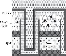
FIGURE 6.16
Structure of capacitor in porous low-k film (CAPL).
A 128 Mbit (32 macros × 4 Mb) embedded DRAM test vehicle reported recently has been considered to be highly manufacturable at 40 nm node level. In logic-based process, only three additional critical masks are required for a low temperature MIM capacitor. Since the macro architecture could operate on a cell capacitance of 10 fF–15 fF because of reduced bit line length, height of capacitor cylinder could also be reduced with consequential advantages. The macro could operate from 25 MHz to 200 MHz which is comparable to SRAM. Using the same MIM eDRAM process, a high-speed designed macro was also shown that could operate on 500 MHz [148].
1. H. Akatsu et al., “A Highly Manufacturable 110 nm DRAM Technology with 8 F2 Vertical Transistor Cell for 1 Gb and Beyond,” VLSI Tech. Dig. Tech Papers, pp. 52–53, 2002.
2. H. Takato et al., “Impact of Surrounding Gate Transistor (SGT) for Ultra High Density LSIs,” IEEE Trans. Electr. Dev., Vol. 38, pp. 573–578, 1991.
3. T. Endoh et al., “2.4 F2 Memory Cell Technology with Stacked-Surrounding Gate Transistor (S-SGT) DRAM,” IEEE Trans. Electr. Dev., Vol. 48, pp. 1599–1603, 2001.
4. H. Sunami et al., “A Corrugated Capacitor Cell (CCC) for Megabit Dynamic MOS Memories,” IEDM Tech. Dig., pp. 806–808, 1982.
5. M. Wada, K. Heida, and S. Watanabe, “A Folded Capacitor Cell (FCC) for Future Megabit DRAMs,” IEDM Tech. Dig., pp. 244–247, 1984.
6. T. Furuyama and J. Frey, “A Vertical Capacitor Cell for VLSI DRAMs,” Symp. VLSI Tech. Dig. Tech. Papers, pp. 16–17, 1984.
7. S. Nakajima et al., “An Isolation Merged Vertical Capacitor Cell for Large Capacity DRAMs,” IEDM Tech. Dig., pp. 240–243, 1984.
8. K. Nakamura et al. “Buried Isolation Capacitor (BIC) for Megabit MOS Dynamic RAM,” IEDM Tech. Dig., pp. 236–239, 1984.
9. M. Nagamoto et al., “A High Density 4M dRAM Process Using Folded Bitline Adaptive Sidewall Isolated Capacitor (FASIC) Cell,” IEDM Tech. Dig., pp. 144–147, 1986.
10. M. Sakamoto et al., “Buried Storage Electrode (BSE) Cell for Megabit DRAMs,” IEDM Tech. Dig., pp. 710–713, 1985.
11. N.C.C. Lu et al., “The SPT Cell—A New Substrate-Plate Trench Cell for DRAMs,” IEDM Tech. Dig., pp. 771–772, 1985.
12. W. Wakamiyia et al., “Novel Stacked Cell for 64 Mb DRAM,” Symp. VLSI Techn. Dig. Tech. Papers, p. 31, 1989.
13. W.F. Richardson et al., “A Trench Transistor Cross Point DRAM Cell,” IEDM Tech. Dig., pp. 714–717, 1985.
14. M. Sakao et al., “A Straight-Line Trench Isolation and Trench-Gate Transistor (SLIT) Cell for Gigabit DRAMs,” Symp. VLSI Techn. Dig. Tech. Papers, pp. 19–20, 1993.
15. Y. Kawamoto et al., “A 1.28 μm2 Bit-line Shielded Memory Cell Technology for 64 Mb DRAM,” Symp. VLSI Tech. Dig. Tech. Papers, pp. 13–14, 1990.
16. W.D. Kim et al., “Development of CVD-Ru/Ta2O5/CVD-TiN Capacitor for Multi Gigabit-Scale DRAM Generation,” Symp. VLSI Technol. Dig. Tech. Papers, pp. 100–101, 2000.
17. C.M. Chu et al., “Cylindrical Ru/SrTiO3/Ru Capacitor Technology for 0.11 μm Generation DRAM,” Symp. VLSI Technol. Dig. Tech. Papers, pp. 43–44, 2001.
18. Y. Fukuzumi et al., “Linear-Supported Cylinder (LSC) Technology to Realize Ru/Ta2O5/Ru for Future DRAMs,” IEDM, pp. 793–796, 2000.
19. K.N. Kim et al., “Highly Manufacturable and High Performance SDR/DDR 4 Gb DRAM,” VLSI Tech. Dig. Tech. Papers, pp. 7–8, 2001.
20. J. Lee et al., “Robust Memory Cell Capacitor using Multi-Stack Storage Node for High Performance in 90 nm Technology and Beyond,” Symp. VLSI Techn. Dig. Tech. Papers, pp. 57–58, 2003.
21. D.H. Kim et al., “A Mechanically Enhanced Storage Node for Virtually Unlimited Height (MESH) Capacitor Aiming at Sub 70 nm DRAMs,” IEDM, pp. 69–72, 2004.
22. J.M. Park et al., “Novel Robust Cell Capacitor (Leaning Exterminated Ring type Insulator) and New Storage Node Contact (Top Spacer Contact) for 70 nm DRAM Technology and Beyond,” Symp. VLSI Tech. Dig. Tech. Papers, pp. 34–35, 2004.
23. J.Y. Kim et al., “The Breakthrough in Data Retention Time of DRAM Using Recessed Channel-Array Transistor (RCAT) for 88 nm Feature Size and Beyond,” Symp. VLSI Tech. Dig. Tech. Papers, pp. 11–12, 2003.
24. J.Y. Kim et al., “S-RCAT (Sphere-shaped-Recess-Channel-Array Transistor) Technology for 70 nm DRAM Feature Size and Beyond,” Symp. VLSI Tech. Dig. Tech. Papers, pp. 34–35, 2005.
25. D. Hisamoto, T. Kaga, and E. Takeda, “Impact of Vertical SOI ‘DELTA’ Structure on Planar Device Technology,” IEEE Trans. Electr. Dev., Vol. 38, pp. 1419–1424, 1991.
26. S.-W. Chung et al., “Highly Scalable Saddle-Fin (S-Fin) Transistor for Sub-50 nm DRAM Technology,” Symp. VLSI Tech. Dig. Tech. Papers, pp. 32–33, 2006.
27. L. Nesbit et al., “A 0.6 μm2 256 Mb Trench DRAM Cell with Self-Aligned Buried Strap (BEST),” IEDM Tech. Dig., pp. 627–630, 1993.
28. U. Gruening et al., “A Novel Trench DRAM Cell with a VERtical Access Transistor and BuriED Strap (VERY BEST) for 4 Gb/1 Gb,” IEDM Tech. Dig., pp. 25–28, 2000.
29. R. Weis et al., “A Highly Cost Efficient 8 F2 DRAM Cell with a Double Gate Vertical Transistor Device for 100 nm and Beyond,” IEDM Tech. Dig., pp. 415–418, 2001.
30. S.Y. Han et al., “A Novel DRAM Cell Transistor Featuring a Partially Insulated Bulk FinFET (Pi-FinFET) with a Pad-Polysilicon Side Contact (PSC),” Symp. VLSI Techn. Dig. Tech. Papers, pp. 166–167, 2007.
31. J.Y. Song et al., “Fin and Recess Channel MOSFET (FiReFET) for Performance Enhancement of Sub-50 nm DRAM Cell,” ISDRS, 2007.
32. W.D. Kim et al., “Development of CVD-Ru/Ta2O5/CVD-TiN Capacitor for Multigigabit-Scale DRAM Generation,” Symp. VLSI Techn. Dig. Tech. Papers, pp. 100–101, 2000.
33. K. Koyama et al., “A Stacked Capacitor with (BaxSri-x) TiO3 for 256 M DRAM,” IEDM Tech. Dig., pp. 823–826, 1991.
34. E. Fujii et al., “ULSI DRAM Technology with Ba0.7Sr0.3TiO3 Film of 1.3 nm Equivalent SiO2 Thickness and 10–9A/Cm2 Leakage Current,” IEDM Tech. Dig., pp. 267–269, 1992.
35. Y. Ohno et al., “A Memory Cell Capacitor with BaxSr1-xTiO3 (BST) Film for Advanced DRAMs,” Symp. VLSI Tech. Dig. Tech. Papers, pp. 149–150, 1994.
36. S. Yamamichi et al., “An ECR MOCVD (BaSr) TiO3 Based Stacked Capacitor Technology with RuO2/Ru/TiN/TiSix Storage Nodes for Gbit-Scale DRAMs,” IEDM Tech. Dig., pp. 119–122, 1995.
37. Y. Nishioka et al., “Giga-bit Scale DRAM Cell with New Simple Ru/(Ba,Sr) TiO3/Ru Stacked Capacitor Using X-Ray Lithography,” IEDM Tech. Dig., pp. 903–906, 1995.
38. A. Yüki et al., “Novel Stacked Capacitor Technology for 1 Gbit DRAMs with CVD-(Ba,Sr) TiO3 Thin Films on a Thick Storage Node of Ru,” IEDM Tech. Dig., pp. 115–118, 1995.
39. H. Yamaguchi et al., “A Stacked Capacitor with an MOCVD-(Ba,Sr) TiO3 Film and a RuO2/Ru Storage Node on a TiN-Capped Plug for 4 Gbit DRAMs and Beyond,” IEDM Tech. Dig., pp. 675–678, 1996.
40. R.B. Khamankar et al., “A Novel BST Storage Capacitor Node Technology Using Platinum Electrode for Gigabit DRAMs,” IEDM Tech. Dig., pp. 245–248, 1997.
41. N. Menou et al., “0.5 nm EOT Leakage ALD SrTiO3 on TiN MIM Capacitor for DRAM Applications,” IEDM Tech. Dig., pp. 1–4, 2008.
42. J.H. Bruning, “Optical Lithography—Thirty Years and Three Orders of Magnitude: The Evolution of Optical Lithography Tools,” Proc. SPIE, Vol. 3051, pp. 14–17, 1997.
43. K.N. Kim et al., “A 0.15 μm DRAM Technology Node for 4 Gb DRAM,” Symp. VLSI Tech. Papers, pp. 16–17, 1998.
44. S. Bukofsky et al., “Extending KrF Lithography to 0.13 μm2 Sub-8F2 DRAM Technology: The Importance of Lithography-Centric Design,” Proc. European Sol. St. Dev., Res. Conf., 2000.
45. K.N. Kim et al., “A 0.13 μm DRAM Technology for Giga Bit Density Stand-Alone and Embedded DRAMs,” Symp. VLSI Tech. Dig. Tech. Papers, pp. 10–11, 2000.
s46. H.S. Jeong et al., “Highly Manufacturable 4 Gb DRAM Using 0.11 μm DRAM Technology,” IEDM Tech. Dig., pp. 353–356, 2000.
47. K. Kim and J.-S. Park, “A 0.11 μm DRAM Technology for 4 Gb DRAM and Beyond,” 6th Int. Conf. Solid State and Integ. Cir. Tech., pp. 178–182, 2001.
48. Y.K. Park et al., “Highly Manufacturable 90 nm DRAM Technology,” IEDM Tech. Dig., pp. 819–822, 2002.
49. H.S. Kim et al. “An Outstanding and Highly Manufacturable 80 nm DRAM Technology,” IEDM Tech. Dig., pp. 17.2.1–17.2.4, 2003.
50. C. Cho et al., “Integrated Device and Process Technology for Sub-70 nm Low Power DRAM,” VLSI Techn. Dig. Tech. Papers, pp. 32–33, 2004.
51. C. Cho et al., “A 6 F2 DRAM Technology in 60 nm Era Gigabit Densities,” Symp. VLSI Techn. Dig. Tech. Papers, pp. 36–37, 2005.
52. M. Fritze et al., “Enhanced Resolution for Future Fabrication,” IEEE Circuits and Devices Magazine, Vol. 19, pp. 43–49, 2003.
53. Y.K. Park et al., “Fully Integrated 56 nm DRAM Technology for 1 Gb DRAM,” Symp. VLSI Techn. Dig. Tech. Papers, pp. 190–191, 2007.
54. H. Lee et al., “Fully Integrated and Functioned 44 nm DRAM Technology for 1 Gb DRAM,” Symp. VLSI Techn. Dig. Tech. Papers, pp. 86–87, 2008.
55. K. Ronse et al., “Lithography Options for the 32 nm Half Pitch Node and Beyond,” IEEE Trans. Circuit and Systems, Vol. 56, pp. 1883–1890, 2009.
56. W.H. Arnold, “Challenges for Lithography Scaling to 32 nm and Below,” Proc. VLSI Techn. Systems and Appl. (VLSI-TSA), 2007.
57. V. Wiaux et al., “A Methodology for Double Patterning Compliant Split and Design,” Proc. SPIE 7140, pp. 71401X–71401X, 2008.
58. A. Bryant, W. Häusch, and T. Mii, “Characteristics of CMOS Device Isolation for the ULSI Age,” IEDM Tech. Dig., pp. 671–674, 1994.
59. T. Hamamoto, S. Sugiura, and S. Swada, “Well Concentration: A Novel Scaling Limitation Factor Derived from DRAM Retention Time and Its Modeling,” IEDM Tech. Dig., pp. 915–918, 1995.
60. B.H. Roh et al., “Shallow Trench Isolation for Enhancement of Data Retention Times in Gigabit DRAM,” SSDM Tech. Dig., pp. 830–832, 1996.
61. K. Kim, C.-G. Hwang, and J.G. Lee, “DRAM Technology Perspective for Gigabit Era,” IEEE Trans. Electr. Dev., Vol. 45, pp. 598–608, 1998.
62. K. Ishimura et al., “Mechanical Stress-Induced MOSFET Punch-Through and Process Optimization for Deep Submicron TEOS-03 Filled STI Device,” VLSI Tech. Dig. Tech. Papers, pp. 123–124, 1997.
63. B. Davari et al., “A New Planarization Technique, Using a Combination of RIE and Chemical Mechanical Polish (CMP),” IEDM Tech. Dig., pp. 61–64, 1989.
64. Y.H. Son, et al., “Highly Manufacturable Device Isolation Technology Using LASER-Induced Epitaxial Growth for Monolithic Stacked Devices,” IEEE Trans. Electr. Dev., Vol. 58, pp. 3863–3868, 2011.
65. K. Kim and M.-Y. Jeong, “The COB Stack DRAM Cell at Technology Node below 100 nm-Scaling Issues and Directions,” IEEE Trans. Semiconductor Manufacturing, Vol. 15, pp. 137–143, 2002.
66. M. Sekine et al., “Self-Aligned Tungsten Strapped Source/Drain and Gate Technology Realizing the Lowest Sheet Resistance for Sub-quarter Micron CMOS,” IEDM Tech. Dig., pp. 493–496, 1994.
67. G.-T. Jeong et al., “A High Performance 16 Mb DRAM Using Giga-Bit Technology,” IEEE Trans. Electr. Dev., Vol. 44, pp. 2064–2069, 1997.
68. R. Mallick et al., “W/WN/Poly Gate Implementation for Sub-130 nm Vertical Cell DRAM,” Symp. VLSI Tech. Papers, pp. 31–32, 2001.
69. S. Choi et al., “Highly Manufacturable Sub-100 nm DRAM Integrated with Full Functionality,” Symp. VLSI Tech. Dig. Tech. Papers, pp. 54–55, 2002.
70. M. Tapajna et al., “Electrical Characteristics of Ru and RuO2/Ta2O5 Gate Stacks for Nanoscale DRAM Technology,” 7th Int. Conf. Adv. Semiconductor Dev. μ-Systems, pp. 267–270, 2008.
71. T. Schloesser et al., “A 6 F2 Buried Word Line DRAM Cell for 40 nm and Beyond,” IEDM Tech. Dig., pp. 1–4, 2008.
72. H. Hada et al., “A Self-Aligned Contact Technology Using Anisotropic Selective Epitaxial Silicon For Gigabit DRAMs,” IEDM Tech. Dig., pp. 665–668, 1995.
73. K.P. Lee et al., “A Process Technology for 1 Giga-Bit DRAM,” IEDM Tech. Dig., pp. 907–910, 1995.
74. H. Koga et al., “A 0.23 μm2 Double Self-Aligned Contact Cell for Gigabit DRAMs With a Ge-Added Vertical Epitaxial Si Pad,” IEDM Tech. Dig., pp. 589–592, 1996.
75. Y.-S. Chun, “A New DRAM Cell Technology Using Merged Process with Storage Node and Memory Cell Contact for 4 Gb DRAM and Beyond,” IEDM Tech. Dig., pp. 351–354, 1998.
76. K. Hinode, I. Asano, and Y. Homma, “Void Formation Mechanism in VLSI Aluminium Metallization,” IEEE Trans. Elect. Dev., Vol. ED-36, pp. 1050–1055, 1989.
77. T. Kikkawa et al., “A Quarter-Micron Interconnection Technology Using Al-Si-Cu/TiN Alternated Layers,” IEDM Tech. Dig., pp. 281–284, 1991.
78. M.T. Bohr, “Interconnect Scaling—The Real Limiter to High Performance ULSI,” IEDM Tech. Dig., pp. 241–244, 1995.
79. A.V. Gelalos et al., “CVD of Copper from a Cu+1 Precursor and Water Vapour and Formation of TiN Encapsulated Submicron Copper Interconnects by Chemical Mechanical Polishing,” Int. Elect. Dev. Tech. Dig., pp. 123–124, 1994.
80. J.S. Kim et al., “A Triple Metallization Technique for Gigabit Scaled DRAM’s,” Proc. VMIC 95, pp. 28–33, 1996.
81. K. Higashi et al., “A Manufacturable Copper/Low-k SiOC/SiCN Process Technology for 90 nm-Node High Performance eDRAM,” IEEE Int. Interconnect Tech. Conf., pp. 15–17, 2002.
82. A. Kajita et al., “Highly Reliable Cu/Low-k Dual-Damascene Interconnect Technology with Hybrid (PAE/SiOC) Dielectrics for 65 nm-Node High Performance eDRAM,” Proc. IEEE Int. Interconnect Tech. Conf., pp. 9–11, 2003.
83. T. Sugiura et al., “45 nm-Node BEOL Integration Featuring Porous-Ultra-Low-k/Cu Multilevel Interconnects,” Proc. Inter. Interconnect Tech. Conf., pp. 15–17, 2005.
84. J. Kawahara et al., A New Direct Low-k/Cu Dual Damascene (DD) Contact Lines for Low Loss (LL) CMOS Device Platform,” Symp. VLSI Tech. Dig. Papers, pp. 106–107, 2008.
85. S. Yokogawa et al., “Analysis of Al Doping Effects on Resistivity and Electromigration of Copper Interconnects,” IEEE Trans. Dev. Mat. Reliability, Vol. 8, pp. 216–221, 2008.
86. H.K. Jung et al., “Formation of Highly Reliable Cu/Low-k Interconnects by Using CVD Co Barrier in Dual Damascene Structures,” IRPS, pp. 307–311, 2011.
87. N. Kwak et al., “BEOL Process Integration with Cu/FSG Wiring at 90 nm Design-Rule DDR DRAM and Their Effect on Field, Refresh Time and Wafer-Level Reliability,” Proc. Inter. Interconnect Tech. Conf., pp. 150–152, 2007.
88. S.M. Rossnagel et al., “Interconnect Issues in Post 45 nm,” IEDM Tech. Dig., pp. 89–91, 2005.
89. J.P. Gambino, “Copper Interconnect Technology for the 22 nm Node,” Int. Symp., VLSI-TSA, pp. 1–2, 2001.
90. S. Nitta et al., “Performance and Reliability of Air Gaps for Advanced BEOL Interconnects,” Interconnect Tech. Conf., pp. 191–192, 2008.
91. K. Ueno, “Material and Process Challenges for Interconnects in Nanoelectronics Era,” Int. Symp. VLSI-TSA, pp. 64–65, 2010.
92. International Technology Roadmap for Semiconductors, 2009, Edition: Interconnects.
93. A. Nieuwoudt and Y. Massoud, “Evaluating the Impact of Resistance in Carbon Nanotubes Bundles for VLSI Interconnect Using Diameter-Dependent Modeling Techniques,” IEEE Trans. Elect. Dev., Vol.53, pp. 2460–2466, 2006.
94. H. Li et al., “Carbon Nanomaterial for Next-Generation Interconnects and Passives: Physics, Status, and Prospects,” IEEE Trans. Elect. Dev., Vol. 56, pp. 1799–1821, 2009.
95. A. Neemi, R. Sarvari, and J.D. Meindl, “Performance Comparison between Carbon Nanotube and Copper Interconnects for Gigascale Integration (GSI),” IEEE Elect. Dev. Lett., Vol. 26, pp. 84–86, 2005.
96. P.G. Collins et al., “Current Saturation and Electrical Breakdown in Multiwalled Carbon Nanotubes,” Phys. Ress. Lett., Vol. 86, no. 14, pp. 3128–3131, 2001.
97. D.K. Brock et al., “Carbon Nanotube Memories and Fabric in a Radiation Hard Semiconductor Foundry,” IEEE Aerospace conf. paper, pp. 1–9, 2005.
98. H. Li et al., “Circuit Modeling and Performance Analysis of Multi-Walled Carbon Nanotube Interconnects,” IEEE Trans. Electr. Dev., Vol. 55, pp. 1328–1339, 2008.
99. B.Q. Wei et al., “Organized Assembly of Carbon Nanotubes,” Nature, Vol. 416, no. 6880, pp. 495–496, 2002.
100. G. Aichmayr et al., “Carbon/High-k Trench Capacitor for the 40 nm DRAM Generation,” Proc. IEEE Symp. VLSI Technol., pp. 186–187, 2007.
101. C. Xu et al., “Graphene Nano-Ribbon (GNR) Interconnects: A Genuine Contender or a Delusive Dream?,” IEDM Tech. Dig., pp. 201–204, 2008.
102. D. Kondo, S. Sato, and Y. Awano, “Self-Organization of Novel Carbon Composite Structure: Graphene Multi-Layers Combined Perpendicularly with Aligned Carbon Nanotubes,” Appl. Phys. Express, Vol. 1, no. 7, p. 074003, 2008.
103. J.W. Ward et al., “Reduction of Interconnect Resistance for the Replacement of Cu for Future Technology Nodes,” IEEE Trans. Nanoelectronics, Vol. 11, pp. 56–62, 2012.
104. S.-N. Pu et al., “Crosstalk Prediction of Single-and Double-Walled Carbon Nanotubes (SWCNT/DWCNT) Bundle Interconnects,” IEEE Trans. Elect. Dev., Vol. 56, pp. 26–37, 2007.
105. T. Mizuno et al., “Si3N4/SiO2 Spacer Induced High Reliability in LDD MOSFET and Simple Degradation MODEL,” IEDM Tech. Dig., p. 234, 1988.
106. K.N. Kim et al., “Highly Manufacturable 1 Gb SDRAM,” Symp. VLSI Tech. Dig. of Tech. Papers, pp. 9–10, 1997.
107. K. Itabashi et al., “Fully Planarized Stacked Capacitor Cell,” Symp. VLSI Tech. Dig. of Tech. Papers, pp. 21–22, 1997.
108. T. Rupp et al., “Extending Trench DRAM Technology to 0.15 μm Groundrule and Beyond,” IEDM Tech. Dig., pp. 33–36, 1999.
109. B.-C. Lee et al., “High Performance Cell Technology Featuring Sub-100 nm DRAM with Multi-Gigabit Density,” IEDM Tech. Dig., pp. 835–838, 2002.
110. Y. Hiura et al., “Integration Technology of Polymetal (W/WSiN/Poly-Si) Dual-Gate CMOS for 1 Gbit DRAMs and Beyond,” IEDM Tech. Dig., pp. 389–392, 1998.
111. J. Amon et al., “A Highly Manufacturable Deep Trench-Based DRAM Cell Layout with a Planar Array Device in a 70 nm Technology,” IEDM Tech. Dig., pp. 73–76, 2004.
112. M. Hamada et al., “A High Performance 0.18 μm Merged DRAM/Logic Technology Featuring 0.45 μm2 Stacked Capacitor Cell,” IEDM Tech. Dig., pp. 45–48, 1999.
113. J.-H. Heo et al., “Void Free and Low Stress Shallow Trench Isolation Technology Using P-SOG for Sub 0.1 μm Devices,” Symp. VLSI Tech. Dig. Tech. Papers, pp. 132–133, 2002.
114. J.H. Lee et al., “Practical Next Generation Solution for Stand-Alone and Embedded DRAM Capacitor,” Symp. VLSI Tech. Dig. Tech. Papers, pp. 114–115, 2002.
115. F. Fishburn et al., “A 78 nm DRAM Technology for Multigigabit Densities,” Symp. VLSI Tech. Dig. Tech. Papers, pp. 28–29, 2004.
116. H. Kim et al., “70 nm DRAM Technology for DDR-3 Application,” Int. Symp. on VSLI Technology (VLSI-TSA), pp. 29–30, 2005.
117. D.-S. Kil et al., “Development of Highly Robust Nano Mixed HfxAlyOz Dielectric for TiN/HfxAlyOz/TiN Capacitor Applicable to 65 nm Generation DRAMs,” Symp. on VLSI Tech. Dig. Tech. Papers, pp. 126–127, 2004.
118. J.W. Lee et al., “Improvement of Data Retention Time in DRAM Using Recessed Channel Array Transistors with Asymmetric Channel Doping for 80 nm Feature Size and Beyond,” E.S.S.D. RC, pp. 449–452, 2004.
119. Kinam Kin, “Technology for Sub-50 nm DRAM and NAND Flash Manufacturing,” VLSI-TSA, pp. 88–94, 2005.
120. Kinam Kim, “Memory Technologies for 50 nm and Beyond,” Solid State and Int. Cir. Tech. (ICS ICT), pp. 685–688, 2006.
121. D.S. Kil et al., “Development of New TiN/ZrO2/Al2O3/ZrO2/TiN Capacitors Extendable to 45 nm Generation DRAMs Replacing HfO2 Based Dielectrics,” Symp. on VLSI Techn. Dig. of Tech. Papers, pp. 38–39, 2006.
122. C.H. Lee et al., “Novel Body Tied FinFET Cell Array Transistor DRAM with Negative Word Line Operation for Sub 60 nm Technology and Beyond,” Symp. VLSI Techn. Dig. Tech. Papers, pp. 130–131, 2004.
123. J.-M. Yoon et al., “A Novel Low Leakage Current VPT (Vertical Pillar Transistor) Integration for 4 F2 DRAM Cell Array with Sub 40 nm Technology,” Device Research Conference, pp. 259–260, 2006.
124. S.-W. Chung et al., “Highly Scalable Saddle-Fin (S-Fin) Transistor for Sub-50 nm DRAM Technology,” VLSI Techn. Dig. Tech. Papers, pp. 32–33, 2006.
125. R. Divakaruni et al., “Technologies for Vertical Transistor DRAM Cells to 70 nm,” Symp. on VLSI Tech. Dig. Tech. Papers, pp. 59–60, 2003.
126. C.-H. Chung et al., “A Novel DRAM Cell Design and Process for 70 nm Generation,” Int. Symp. on VLSI Tech. Sys. and Appl., pp. 1–2, 2006.
127. W. Mueller et al., “Challenges for the DRAM Cell Scaling to 40 nm,” IEDM Tech. Dig., pp. 226–230, 2005.
128. W. Mueller et al., “Trench DRAM Technologies for the 50 nm Node and Beyond,” Int. Symp. on VLSI Tech. Sys. and Appli., pp. 1–2, 2006.
129. L. Heineck et al., “A Novel Cell Arrangement Enabling Trench DRAM Scaling to 40 nm and Beyond,” IEDM Tech. Dig., pp. 31–32, 2007.
130. D.K. Schulz and N. Wehn, “Embedded DRAM Development: Technology Physical Design, and Application Issues,” IEEE Design and Test of Computer, pp. 7–15, 2001.
131. S. Natrajan et al., “Searching for the Dream Embedded Memory,” IEEE S.S. Circuit Magazine, pp. 34–44, 2009.
132. T. Yoshida et al., “A Fabrication Method for High Performance Embedded DRAM of 0.18 μm Generation and Beyond,” IEEE Custom Integ. Cir. Conf., pp. 61–64, 2000.
133. H. Ishiuchi et al., “Embedded DRAM Technologies,” IEDM Tech. Dig., pp. 33–36, 1997.
134. H. Takato et al., “Embedded DRAM Technology: Past, Present, and Future,” Int. Symp. VLSI Techn., System & Appl., pp. 239–242, 1999.
135. M. Togo et al., “A Salicide-Bridged Trench Capacitor with a Double-Sacrificial-Si3N4-Sidewall (DSS) for High-Performance Logic-Embedded DRAMs,” IEDM Tech. Dig., pp. 37–40, 1997.
136. M. Matsubara et al., “Fully Compatible Integration of High Density Embedded DRAM with 65 nm CMOS Technology (CMOS5),” IEDM Tech. Dig., pp. 423–426, 2003.
137. T. Sanuki et al., “High Density and Fully Compatible Embedded DRAM Cell with 45 nm CMOS Technology (CMOS6),” Symp. VLSI Techn. Dig. Tech. Papers, pp. 14–15, 2005.
138. G. Wang et al., “A 0.127 μm2 High Performance 65 nm SOI Based Embedded DRAM for On-Processor Applications,” IEDM Tech. Dig., pp. 1–4, 2006.
139. R. Kalla et al., “Power 7™: IBM’s Next Generation POWER Microprocessor,” Hot Chips, 2009.
140. G. Wang et al., “Scaling Deep Trench Based eDRAM on SOI to 32 nm and Beyond,” IEDM Tech. Dig., pp. 259–262, 2009.
141. J. Barth et al., “A 500 MHz Random Cycle 1.5 ns Latency, SOI Embedded DRAM Macro Featuring a 3T Micro Sense Amplifier,” I.SSCC Dig. Tech. Papers, pp. 486–487, 2007.
142. M. Yoshida et al., “An Embedded 0.405 μm2 Stacked DRAM Technology Integrated with High Performance 0.2 μm CMOS Logic and 6-Level Metallization,” IEDM Tech. Dig., pp. 41–44, 1999.
143. S. Arai et al., “A 0.13 μm Full Metal Embedded DRAM Technology Targeting on 1.2V, 450 MHz Operation,” IEDM Tech. Dig., pp. 403–406, 2001.
144. Y. Aoki et al., “Ultra-High Performance 0.13 μm Embedded DRAM Technology Using TiN/HfO2/TiN/W Capacitor and Body-Slightly-Tied SOI,” IEDM Tech. Dig., pp. 831–834, 2002.
145. Y. Yamagata et al., “Device Technology for Embedded DRAM Utilization Stacked MIM (Metal-Insulator-Metal) Capacitor,” IEEE Custom Integ. Cir. Conf. (CICC), pp. 421–427, 2006.
146. S. Cremer et al., “COLK Cell: A New Embedded DRAM Architecture for Advanced CMOS Nodes,” Proc. European Solid-State DRC (ESSDRC), pp. 158–161, 2010.
147. K. Hijioka et al., “A Novel Cylinder-Type MIM Capacitor in Porous Low-k Film (CAPL) for Embedded DRAM with Advanced CMOS Logic,” IEDM Tech. Dig., pp. 756–759, 2010.
148. C.Y. Chen et al., “A High-Performance Low-Power Highly Manufacturable Embedded DRAM Technology Using Backend Hi-K MIM Capacitor at 40 nm Node and Beyond,” Symp. VLSI Techn. System & Appl., pp. 58–59, 2011.