
Continued reduction of minimum feature size and the advancements in the fabrication processes were the main reasons for the DRAM density enhancement. As soon as multi-megabit DRAM appeared on the horizon, it opened completely new application areas for the DRAMs. The use of megabit DRAMs in portable equipment, which required low-voltage operation, such that they could operate on battery for longer duration, became highly desirable. At one point in time, a 5 V supply was standard but was not suitable for long-term battery-based operation. In the low-voltage operating range a 1.5 V DRAM given by M. Aoki and others [1] was one of the first such DRAMs. It also reduced power consumption as bit line swing was reduced only up to the sum of the threshold voltages for NMOS and PMOS transistors in the sense amplifier. A 2 Kbit test DRAM worked successfully at the reduced voltage, and calculated value of the operating current was shown to be reduced from 15 mA at 5 V to less than a third of its value and the DRAM was expected to operate for 500 hours on eight 2-ampere-hour dry batteries. At this stage, reduction in supply voltage created two major problems: (1) decrease in signal-to-noise (S/N) ratio, and (2) degradation in operating speed. Soon after, a major breakthrough came in the form of another landmark 1.5 V DRAM, at 64 Mbit level with increased S/N ratio, given by Nakagome and others [2], using 0.3 μm triple-well CMOS process with no back-gate bias. The new DRAM used three new circuit modifications for making it operative at low voltage with improved performance. It used an I/O sense amplifier circuit with complementary sensing scheme having PMOS-driven current sense amplifier and NMOS read-out gates. From word line swing to bit line swing, a boost ratio of more than 1.75 was needed for low-voltage operation of 1.5 V; hence, a new feedback charge pump circuit was used. To improve S/N ratio, an accurate and highly regulated half-Vcc voltage level was also used. All these features resulted in an RAS access time of 50 ns and power dissipation was only 44 mW with active current of 29 mA and standby current of 1 mA at room temperature.
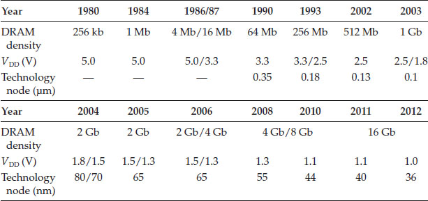
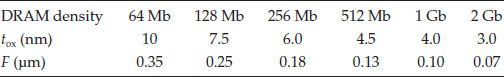
In stand-alone commercial DRAMs, standard supply voltage VDD was reduced to 1.8 V by 2004 and trend is to continuously decrease it [3]. Table 7.1 shows trend in supply voltage with DRAM density over the years. For eDRAMs the voltage was to be lowered even more as it had to be compatible with surrounding peripherals and logic and its suitability with the use of single NiCd cell having a minimum level of supply voltage of 0.9 V only [4]. At the same time advances in technology forced DRAM cell area along with its storage capacitor size to continuously decrease through using innovative cells and reduction in the technology node, and resulting in increased DRAM density accompanied with decrease in gate oxide (tox) thickness bringing a host of challenges to be taken up. Table 7.2 shows the trend of decreasing tox with DRAM density. Increased DRAM density meant, more number of cells on a single bit line, which increased bit line capacitance CBL, resulting in reduced charge transfer ratio (CS/(CS + CBL) ≈ CS/CBL), which would result in unreliable performance in presence of soft errors and other noises unless measures were taken. Another cause of unreliable operation and variable response was the variation in physical dimensions and resultant variations in the characteristics of DRAM cell transistors and capacitors and transistors used elsewhere on the chip. As with other parameters, it caused varied values of threshold Vth on the same chip. It affected the performance in different ways depending on the use of transistors. However, a more serious problem was the increase in power dissipation due to the increase in leakage currents, both in the active and inactive condition of a cell, module, or block. This chapter will discuss the ways in which the challenges that arose in designing low-voltage/low-power DRAMs were faced and the problems resolved especially with regard to power dissipation.
Predominantly Used Supply Voltage and Adopted Technology Node and (Expected) Progress with DRAM Density
Source: Y. Nakagome, et al., “Review and Future Prospects of Low-Voltage RAM Circuits,” IBM J. Res. and Dev., Vol. 47, no. 5/6, pp. 525–552, 2003; International Technology Roadmap for Semiconductors, http://public.itrs.net/Files/2001.ITRS/Home. hlm, 2001 Edition; and ITRS 2009.
Change in Gate Oxide Thickness with Increase in DRAM Density
A closely related issue is reducing the data retention power in DRAMs. Because of inherent leakages and destructive nature of READ operation, continuous refresh also requires power. This requirement of data retention power is necessary to be reduced for battery backup-based operations. Continuous efforts have been made in this direction. Before discussing the techniques/circuit solutions or technological advancements for reducing leakage current and improving data retention time, different kinds of leakages for DRAM cells and peripherals are discussed.
A DRAM chip can broadly comprise (1) the memory cell array, (2) row and column decoders, and (3) other peripheral circuits. Each component has undergone some changes from its basic form over the years. However, there are several reasons for leakages due to which the stored signal changes and power is dissipated irrespective of the modifications in the DRAM chip components: Some of the significant ones are as follows [5]:
1. Reverse-biased junction leakage current from the storage node
2. Sub-threshold leakage current of the access transistors
3. Capacitor dielectric leakage current
4. Gate-induced drain leakage current (GIDL) at the storage node
5. Gate dielectric leakage current
6. Leakage current between the adjacent cells
While the total leakage current is the sum of all leakage currents, each of the above mentioned components has different weight and their weight has varied considerably with the changes in the technologies, fabrication processes, minimum feature size and the supply voltage. Moreover, all the peripheral circuits, like row and column decoders, sense amplifiers, voltage up/down converters, refreshing circuit, etc. do have similar types of leakages, and power is needed to recover the leaked charge as well as for the normal functioning of the DRAM cell and peripherals.
7.2.1 Junction Leakage and Sub-Threshold Currents
Leakage current flows through the reverse-biased p-n junctions wherever these are located on the chip. For the sub-micron feature size, leakage current is in the range of few pA/μm2 at room temperature and the total contribution may not be very high. However, the junction leakage currents increase exponentially with junction temperature, due to the thermally generated carriers. Hence, keeping the operating temperature low is highly desirable to keep this kind of leakage under control. Another important source of leakage is sub-threshold current of the transistors on the chip. Drain-to-source current does flow in MOSFETs when gate-to-source voltage VGS is less than its threshold voltage Vth and even when VGS = 0. The closer is the threshold voltage to zero volts, the larger is the leakage current, and the larger is the static power consumption. Standard practice to keep sub-threshold leakage small is to keep Vth not below 0.5 V–0.6 V or even higher (~0.75–1.0 V); though, keeping Vth high becomes a problem with reduced supply voltage VDD. Transistors fabricated through such technologies which produce sharper turn-off characteristics (VDS ∼ ID) are preferable, to reduce sub-threshold current.
The junction leakage current from the storage node is a dominant component among all the possible leakages when boron concentration of p-well is increased and the working temperature rises. However, this increased leakage could not be accounted for with normal reasons, that is, diffusion current and generation–recombination current, as both of these are inversely proportional to the boron concentration of the p-well [6]. The anomalous situation is well characterized by thermionic field emission (TFE) current, which has an exponential relationship to the activation energy at the deep level. Thermionic emission from a deep level is enhanced by the tunneling effect due to the strong field in the depletion region [5]. As this increased electric field is due to the enhancements of substrate doping, junction leakage current can be reduced by lowering the substrate doping to an optimum level, keeping in mind that it will affect the sub-threshold characteristics of the transistor.
Gate tunnel leakage current is the sum of the leakage currents through the dielectrics of the gates of all transistors on the chip. This kind of leakage becomes a problem around 3 nm gate oxide thickness (tox) and increases after that at a rate of one order with tox decrement of only 0.2 nm [7]. As the DRAM cells needed a high operating voltage (because of larger Vth) for stable memory operation, tox of standard DRAMs has not been reduced as fast as the rate for static RAMs. A thinner tox could be used for peripheral circuits as these could operate on low voltage, though normally same gate oxide thickness transistors were preferred and used on the whole chip. However, for eDRAMs, a dual-VDD and dual-tox device approach has also been adopted for getting higher speeds, and it is expected that even stand-alone DRAMs would use dual-tox approach [8]. Different solutions have been proposed to reduce the leakage, such as shutting off the supply path by inserting a power switch [9]; however, these are applicable for standby mode and shall be discussed later.
7.3 Power Dissipation in DRAMs
Irrespective of the nature of leakage currents (charge) and their weights, power has to be supplied to the DRAM, which, along with the normal chip-functioning requirement, shall also include the power dissipated due to the leakage currents. For discussing different components of power dissipation, Figure 7.1 shows a simplified chip architecture displaying three major blocks of cell array, row/column decoders, and peripherals. Here the core cell array is comprised of m cells in a row with n number of rows. In the simplified form one word line having m cells is activated and the remaining m(n – 1) cells remain unselected. For a CMOS DRAM total power consumption shall be P = VDD IDD, where IDD, the total chip current, shall be the sum of the following components [9]:
(7.1) |
(7.2) |
(7.3) |
(7.4) |
(7.5) |
In Equations (7.1) to (7.5), iact and ihld are the effective currents in active/selected cells and effective data retention current of inactive/nonselected cells, respectively. CDE is the output node capacitance of each decoder, Vint is the internal supply voltage, IDCP is the total static or quasi-static current of periphery, and f is the operating frequency being equal to (1/tRC) with tRC being the cycle time. The working frequency (or tRC) has considerable impact in changing the weights of different components in the power requirement. At the same time, levels of Vint and threshold voltage of transistors Vth do affect the power component requirement ratio. For example, for Equation (7.3), the decoder charging current may become negligible when a CMOS NAND decoder is used because only one each of the column and row decoders is operative, hence (n + m) is replaced by 2 only [10]. As far as Equation (7.5) is concerned, IDCP is mainly due to the on-chip voltage converters of different types. With efficient design, its contribution can become small and shall remain constant even with increasing value of f. Ordinarily, the component could have been neglected below gigabit range DRAMs; however, for low-voltage, low-power DRAMs, special efforts are needed to control this component. A discussion of on-chip voltage converters is included in Section 7.7. Even for megabit-density DRAMs, the data retention current given by Equation (7.2) was small at high frequencies in comparison to other components, but not for gigabit DRAMs. Considerable effort is now being made to contain the data retention current; the issue shall be discussed in latter parts of the chapter.
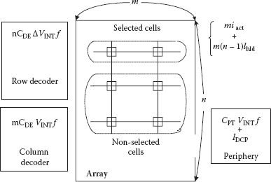
FIGURE 7.1
Important current components for power dissipation in a DRAM chip. (Redrawn from “Trends in Low-Power RAM Circuit Technologies”, K. Itoh, K. Sasaki and Y. Nakagome, Proc. IEEE, Vol. 83, No,4, pp. 524–543, 1995.)
A sense amplifier is a necessity for a DRAM cell for the refreshing process, wherein bit line is charged and discharged with a relatively large swing ΔVBL, with charging current of (CBL ΔVBL* f), where CBL is the bit line capacitance. At higher operating frequency f, power requirement components depending on it become large and while neglecting smaller components, can be combined and approximated as
(7.6) |
Expressions for the DRAM power requirement from Equations (7.1 to 7.6) show obvious ways of reducing it. Reduction in charging capacitances m CBL and CPT and lowering of external and internal voltages VDD, Vint, and ΔVBL need careful consideration; however, reduction of bit line dissipation charge (mCBL ΔVBL) needs special attention as it dominates the total active power.
Sufficient signal-to-noise (S/N) ratio must be maintained for reliable DRAM operation as the cell signal is small in magnitude and resides on the floating bit line, which itself is susceptible to noise. Charge transfer ratio between a cell and a bit line is equal to CS/(CS + CBL), where CS is the storage cell capacitance. Hence generated signal vS for the half-VDD precharging scheme is expressed as
(7.7) |
where QS = CS. ΔVBL is the cell signal charge. Hence reduction in CBL is advantageous in two ways; it reduces IDD while increasing signal vS. Whereas reducing ΔVBL reduces IDD but degrades the signal charge [4].
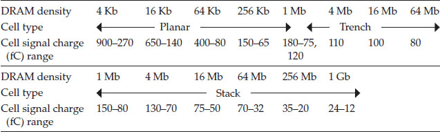
Magnitude of the signal charge has been reduced considerably with the increase in DRAM capacity, mainly due to reduction in the minimum feature size (F) and supply voltage reduction, and the type of cell, as shown in Table 7.3. It is important to keep QS above a critical value for reliable DRAM operations that should make ΔVBL distinct from the memory array noise and soft errors. Value of QS is also affected due to higher Vth, Vth variation, and Vth mismatch among devices. Increasing the value of Vth is a necessity when the memory capacity is increased, even with lower VDD, because the maximum refresh time, tREFmax, of DRAM must increase with the memory capacity as mentioned in Section 7.6.1.1. Variations in Vth change the half-VDD sensing in DRAM and Vth mismatch between cross-coupled MOSFETs present in large number of DRAM sense amplifiers also increases with increased memory capacity and decreased F; that further degrades the sensing signal of the DRAMs. Calculated maximum Vth mismatch in NMOS used in the DRAM sense amplifiers is shown in Table 7.4; it also shows improvement while using redundancy [8]. The mismatch is doubled with F changing from 0.35 μm to 0.07 μm. Though not a very serious problem for DRAM around 0.1 μm technology, it becomes serious with further small values of F, due to high process sensitivity. One of the main problems created by transistor mismatch (along with the bit lines deviating from design characteristics) is the development of offset noise. An offset-compensating bit line sensing was proposed in [11] but could not be applied to commercial DRAMs because the proposed compensating circuit was too large to fit in the cell pitch. Another offset cancellation sense amplifier, which could shrink to fit in the cell pitch, was also proposed [12]. However, it uses extra chip area and consumes extra time for offset cancellation before the word line activation can cause significant reduction in sensing speed. The large current drawn by differential amplifiers is an additional problem. Direct current sensing technique improves sensing performance by removing timing constraints of column-select line signals, but the low-voltage operation requires a multistage amplification, because of small value of ΔVBL [13]. An offset compensated pre-sensing scheme was employed along with the direct sensing scheme, which effectively reduces the total time for the read operation [14]. However, it requires additional charge pumping for possible leakage of the boost voltage source for equalization and needs at least 3% chip size overhead.
Cell Signal Charge Range Variation with DRAM Density and Cell Type
Maximum Vth Mismatch without and with Redundancy
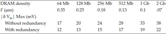
Use of column-redundancy technique seems a better option for overcoming the Vth mismatch/offset noise problem as it can replace a certain percentage of sense amplifiers with excessive variation in Vth (δVth). For example, if the ratio of spare columns to normal columns is 1/256 (0.4% of area), memory capacity limitation is extended by at least three generations [8]; Table 7.4 shows advantage of using redundancy for reducing Vth mismatch. An efficient test method to detect and replace defective sense amplifiers or excessive δVth sense amplifier is also needed. On chip error-checking and correcting (ECC) schemes are almost essential and shall be taken up separately.
7.5 Power Dissipation for Data Retention
While the DRAM is in data retention mode, the refresh operation retains the data. In normal course, m cells of a word line are read simultaneously and restored. The process is done for the n word lines. Obviously n also becomes the number of refresh cycles and current given by Equation (7.6) flows during every cycle. The frequency f at which the current flows is (n/tREF), where tREF is the refresh time of cells in the retention mode and reduces with increasing junction temperature. So, from Equation (7.6), data retention current is given as [4]
(7.8) |
When the DRAM is in the active mode, cell leakage current and junction temperature become maximum. Hence refreshing of the cell is required at a very high rate and tREF becomes tREF max, which makes it much smaller than tREF. Thus, IDCP becomes relatively small in active mode but becomes larger than AC current component because of small (n/tREF) during refresh-only duration and it also needs minimization.
The necessity for reduction in power consumption on a DRAM chip cannot be overemphasized. Continuous attempts have been made to decrease it on the face of increasing memory density and capacity. At each generation low-power circuits have been developed and combinations of technology developments have resulted in a downward trend in power consumption [4]. Continued reduction in power dissipation could become possible mainly with the applicability of the following:
1. Partial activation of multi-divided bit line and shared input/output
2. Use of CMOS technology in place of NMOS technology, including half-VDD bit line precharging of the bit line
3. Reduction in the supply voltage (VDD) and use of on-chip voltage converters
7.6.1 Bit Line Capacitance and Its Reduction
Figure 7.2 shows basic architecture of a (m × n) DRAM array comprised of m columns and n rows with k subarrays. The rows have been divided such that each subsection has (n/k) rows, thereby dividing the bit-line capacitance to a manageable value. All the m cells connected to a word line are refreshed simultaneously, and the process is repeated sequentially for the remaining (n – 1) rows one at a time, without selecting a bit line. For proper functioning (i.e., to avoid conflict with refreshing process), normal READ/WRITE operation is done during the rest period. However, a successful refresh operation needs to be performed for each row within the maximum allowable refresh time, tREF max, which depends on the maximum leakage current of the memory cell; the maximum refresh cycle time is (tREF max/n).
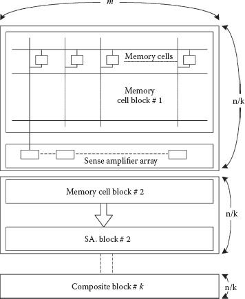
FIGURE 7.2
Basic architecture of an m * n DRAM core with subdivided k arrays. (Redrawn from “Trends in Megabit DRAM Circuit Design”, K. Itoh, IEEE J. Solid-State Circuits, Vol. 25, No. 3, pp. 778–788, 1990.)
As the memory capacity (m*n) increases, the rows are further divided, that is, k is increased to limit (n/k), or in other words to keep the bit line capacitance CBL within safe bounds. It results in a sharp rise in the number of amplifiers used on the chip, m*k; a 1 Gbit chip may require even a million amplifiers. The reason behind the increase in the number of sense amplifiers was that in the initial scheme one sense amplifier at each column decoder division of sub-block was used as shown in Figure 7.2. In another approach, called shared sense amplifier scheme, which was in practice at 256 Kbit–4 Mbit DRAM capacity level, two sub-data lines were allowed to share one sense amplifier [15,16]. In this scheme cell signals become double as the bit line capacitance becomes half the conventional scheme. There was reduction in chip size because of reduced number of sense amplifiers and associated circuitry and hence power consumed in sense amplifiers was also reduced. However, drawback of power dissipation due to bit line capacitance still remained equal to the conventional case because for the purpose of (dis) charging the bit lines, there was no change. This line of action exhausted its usefulness at 16 Mbit DRAM level with combined use of shared sense amplifier, shared I/O, and shared column decoders; an arrangement is shown in Figure 7.3. Advantage of using shared I/O is that it further halves the multi-divided bit line [17]. Only one sense amplifier is activated along the bit line to achieve its partial activation, which lowers the power dissipation. More reduction in power is achieved by increasing the value of n, as discussed later.
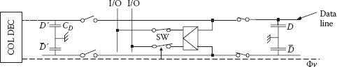
FIGURE 7.3
Memory array organization for showing shared column decoder. (Modified from “An Experimental 1 Mb DRAM with On-Chip Voltage Limiter”, K. Itoh et al., ISSCC, pp. 282–283, 1984.)
In addition to the division of bit line, a multi-divided word line structure is also available. In hierarchical word line structure, a word line is divided into a few sub-word lines; hence partial activation of word lines becomes possible. Though the architecture has some speed performance drawback, it has great potential for power reduction [18]. The architecture can easily reduce chip power dissipation to half.
Use of partial activation of multi-divided data line reduces its effective charging capacitance, but word line length m is not reduced without increasing tREFmax of the cell. To know the reason for it, the refresh-busy rate γ, expressed in Equation (7.9), needs a bit of consideration [16]:
(7.9) |
Here M and tRCmin are the memory capacity and the minimum cycle time, respectively, and it is better to have smaller γ for having larger active time. Hence, for a given DRAM capacity M and fixed tRC min, it is necessary to maintain the product of m and tREF max, which will keep γ constant. For increased capacity of DRAM, m ∗ tREF max shall have to be increased proportionally. Normally m and tREF max are increased in the same proportion, to have a compromise between cell array power consumption and the cell leakage current. Value of tREF max has been doubled at each generation though it is difficult to maintain in practice because of its dependence on the cell leakage current [19]. Hence one of the solutions is to use a new refreshing scheme that employs multi-divided word line [18]. With divided word line, given that m is reduced, maximum power consumption is reduced, which can allow increased tREF max. More recent methods of improving refresh time shall be discussed in Section 7.8.
CMOS technology has shown conclusively that its application reduces power dissipation. For DRAMs, there are different reasons which combine together, like use of half-VCC (array voltage) bit line precharging, and use of CMOS peripheral circuits. For example, as in Equation (7.7), generated cell signal vS has been derived assuming half-VDD (supply voltage) precharged bit line, has become a standard practice now. Charging and discharging of bit lines need reduced power as the precharge voltage is not through the charging of bit lines to VDD but due to the charge sharing between two halves of the bit line. In addition, peak currents are nearly halved while sensing and precharging. It results in narrow supply lines decreasing parasitic capacitance of the wiring, which not only makes the DRAM cell fast but also reduces the generated noise.
For the NMOS case, all row decoders except the one selected were discharged from the precharge voltage, whereas for the CMOS case only one selected decoder is discharged and all the rest of the decoders remain at the precharge level. This results in a sharp decrease in power dissipation for CMOS decoders and could reach 4% of that in NMOS in normal course [10]. Peak current is also reduced to nearly half that of NMOS case, with consequential advantage.
Clock generators are essential components on DRAM chips. CMOS clock generators have been shown to consume about half the power (of NMOS clock generators) including the dissipation for (dis) charging the load capacitance. CMOS clock generators have smaller node capacitances and occupy nearly half the chip area compared to usual NMOS circuits, on account of simpler circuitry. It all results in lower power consumption [10].
7.6.3 On-Chip Voltage Reduction/Conversion
For NMOS DRAMs normal supply voltage was +12 V in the early 1970s, which soon changed to 5 V for CMOS DRAMs for better reliability and the minimization of hot electron injections through gate oxide. It was essential to standardize it from the point of view of IC manufacturers as well as users. Around 64 Mbit DRAM density levels it became obvious to the manufacturers that continuation of single supply voltage, VDD of 5 V was not feasible on twin counts of excessive power dissipation and the scaling down of the transistors on the chip. Although practically it was also not possible to reduce supply voltage with each generation of reduced minimum feature size of the transistor, it was predicted very early that beyond 1 Mbit, it would be very difficult to reduce power dissipation without further reducing supply voltage. From the early 1990s, with 1.5 V DRAMs design for mobile device applications, sharp reduction in the voltage was foreseen. At the same time at low operating voltage of bit line (which was further reduced because of VCC/2 level precharging), it becomes necessary to increase the word line voltage even above VCC for overcoming the threshold offset voltage. A back-bias voltage (changing with the DRAM generations) was also needed on the chip. Conversion to up and down fluctuations of the standard power supply becomes essential for reducing power consumption and reliable operation. A large number of circuits/techniques are now available for this purpose and shall be discussed in Section 7.7.
At 64 Kbit DRAM density level even when supply voltage was reduced to 5 V, disturbance due to noise was not prohibitive. Architecture was simple NMOS, full VDD precharge and open bit line with enough spacing between bit lines. With DRAM density moving into Mbit range spacing between bit lines decreased, giving rise to large coupling capacitance. Introduction of CMOS technology led to lower power consumption DRAMs and then to low voltage battery-operated systems, which reduced the amount of cell signal, which was already reduced with ½ VCC precharge scheme. With the generation of larger noises and reduction of cell signal, signal-to-noise ratio started to decrease rapidly. At 4–16 Mbit stage, it became clear that unless measures were taken, differentiation of noise from signal would become difficult. The second half of the 1980s saw a lot of activity in the study of different noises on the DRAM chip and efforts in improving SNR; either cell signal was increased or noises were decreased.
For signal improvement, charge transfer (~Cs/CBL), was maintained by increasing the storage capacitance Cs, through the use of three-dimensional capacitors like trench or stacked capacitors and later on other advanced versions and techniques like hemispherical grains and use of high permittivity dielectric. However, a limit of 25–30 fF was considered practically safe and the bit line capacitance CBL was tried to be reduced. Half-VCC precharging was also an important scheme for enabling doubled storage capacitance for a fixed electric field across the capacitor insulator [19]. Multidivision of data lines in blocks, as discussed in Section 7.6.1, was found essential in this regard. Reduction in bit line wire width reduced CBL; however, interbit capacitance increased when the DRAM density increased as spacing between bit lines decreased.
With storage capacitance Cs remaining almost constant, and CBL also nearly same within practically reducible limits, only choice was to reduce noises of all types, which continued to increase with rise in DRAM density.
Around 16 Mbit DRAM density, coupling or interference to noise became a major problem in realizing high-speed, high-density DRAMs. There were mainly two types of noises, due to interbit line (BL) coupling capacitance and BL-word line (WL) feedback noise in the access transistor. Inter-BL coupling noise was originating because of signals in adjacent BL pairs and intrapair coupling noise was between true and complementary BLs. A twisted bit line (TBL) scheme in which BLs are divided in four sections with each BL pair twisted two times and a modified twisted bit-line (MTBL) scheme in which BLs are not placed adjacent to their pair BL, in addition to the twisting like that in TBL, eliminated inter-BL coupling noise and claimed to have eliminated intra-BL coupling noise as well [20,21]. The TBL and MTBL schemes were applicable to both the open and folded BL approaches, where BLs are equally divided into four sections and each BL pair is twisted at two of the four boundary points of the sections.
The TBL scheme has been used in some DRAM chips [21,22], but it could not suppress intra-BL coupling noise and required additional chip area for dummy cells and BL twisting. In addition, the signal loss in a 1 Gbit DRAM is estimated to be >30% of total signal. To overcome these limitations multiple TBL has been proposed [23]. It eliminated both the inter-and intra-BL coupling noise but imposed extreme constraints on chip design and required special process and design technologies, and it could not be applied to the folded-bit line arrangement, commonly used in DRAMs. In a different technique, a data-line shielded stacked capacitor (STC) cell was employed in which position of the data line was changed with respect to the storage and plate layer, compared to earlier STC cells; the data-line is shielded by either the storage or the plate layer [24]. Interference noise was reduced below 7% at 2.8 μm data-line pitch, without transposing the pair of data lines. Extra chip area was not needed.
The capacitor-over-bit-line (COB) cell structure suppresses the inter-and intra-BL interferences, but its fabrication process was considered difficult. Storage node contact formation needed small and deep contact node etching along with a large topology difference between the cell array and the peripherals, which was expected to be more pronounced in gigabit range [25]. Another modified twisted bit-line scheme (MTBL) structure was proposed to overcome the problems of earlier TBL schemes and the COB structure. Figure 7.4(a) shows one of the structures proposed [26,27] in which twisting of BLs is done in a different way. Hence, the inter-BL interference is converted into common mode noise and the intra-BL noise is suppressed by a shielding effect. The twisting can be applied to any BL precharging scheme, and compared to conventional folded bit line proposed twisting reduced 50% of inter-and intra-BL noise. The scheme does not need any special layout and/or sense amplifier and can be applied to open BL structure with same benefits. Further improvement in noise reduction is possible by twisting sets of six or eight BLs as shown in Figure 7.4(b) and (c). Resultant reduction in noise by approximately 66% and 75%, respectively, is possible by twisting the sets of six or eight BLs.
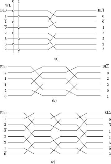
FIGURE 7.4
MTBL configuration having (a) four BLs with single twisting, (b) six BLs with double twisting, and (c) eight BLs with triple twisting. (“Multiple Twisted Data Line Techniques for Multigigabit DRAMs”, D.-S. Min and D.W. Langer, IEEE J. Solid State Circ., Vol. 34, pp. 856–865, 1999.)
In high density DRAMs, word line coupling noise also becomes troublesome mainly because of higher WL voltage than supply voltage and metal WL strapping. Even for the DRAMs with sub-WL driver schemes, with scaled down threshold voltage and supply voltage, WL coupling can become more problematic than BL-coupling noise. Similar to MTBL, a multiple twisted word-line (MTWL) scheme has been effectively used. Four WLs are twisted at the center of the WLs in the same way as it was done for BLs shown in Figure 7.4. It reduces the effective coupling capacitance of adjacent WLs. While twisting, two WLs are separated by two WL pitches, considerably reducing capacitance coupling [27]. A 256 Mbit DRAM was fabricated, with transistor threshold Vth = 1.0 V, sheet resistance of 25 and 0.07 Ω/sq. for polycide and metal WLs, respectively, and noise-to-signal ratio (NSR) was simulated and measured for the cases using (1) conventional WL, (2) proposed MTWL, and (3) combined MTWL and MTBL. Value of NSR increases rapidly as WL pitch is scaled down. For WL pitch of 0.37 μm in case of 1 Gbit DRAM level, NSR is 23% for the convention WL scheme, which when combined with BL coupling noise becomes unacceptably high for a functional DRAM. With MTWL scheme, 35% reduction in NSR is achieved in comparison to the conventional WL. For a 256 Mbit DRAM case combinations of MTWL and MTBL schemes achieved a 64% reduction in NSR compared to the conventional WL and TBL implementation.
7.7 On-Chip Voltage Converter Circuits
Operation of DRAMs at low voltage became an extremely important requirement to save power consumption. It was also essential for maintaining reliability of the DRAMs. With continued reduction in oxide film thickness (tox), excess electrical stress had to be avoided and generation of hot electrons was to be minimized. With successive technology generation, internal chip voltages were different and their ratio with supply voltage continued to change. At the same time standardization of supply voltage could not be done too frequently. Only the on-chip voltage converters reconciled the conflicting requirements; hence became essential. For example, supply voltage was converted on chip to nearly 2.5 V for 64 Mbit DRAM having tox = 10 nm, which was further reduced to 2–2.5 V and 1.5–1.8 V for 256 Mbit and 1 Gbit level DRAMs [28]. Another extremely important reason for further reduction in operating voltage was the DRAM demand for battery operated hand-held mobiles and digital devices. On the other hand, voltage boosting was needed for the word line, and other on-chip voltage levels were needed for half-VCC operation of bit line, back-bias voltage, and so on.
Probably the first circuit of an on-chip supply voltage converter for DRAMs was given by Mano and others in 1983 for immunizing MOS transistors from hot carrier injections [29]. A 5 V supply was converted to 3 V for cell array circuitry and the rest of the peripheral and interface worked on 5 V. Soon a voltage converter was given by Itoh and others as shown in Figure 7.5, in which limiter block converted VDD to VL (nominal value 3.7 V) and the word line voltage was (VL + Vth). Bit line was precharged to VL (not VCC/2) and precharge clock also received (VL + Vth). A charge pump was used to generate VCC + 2Vth for the voltage limiter. For on-chip voltage down converter (VDC), it is extremely important to provide regulated and accurate voltage when large DRAM array current changes from zero to peak and vice-versa. The VDC should also be suitable against changes in external power supply and temperature. At the same time, it is also important to have a provision of on-chip burn-in capability. Figure 7.6 shows an early VDC, which basically consisted of a current mirror differential amplifier and common source output transistor [30] and converts 5 volts VDD to a stable 3.3 V. Gate width of the output transistor has to be very large and the gate voltage has to respond quickly when the output goes low; VDC needs larger value of amplifier current. The bias current is needed to minimize output voltage deviation when the load current becomes nearly zero. An important requirement of the on-chip voltage converter circuits is that the reference voltage VREF must be accurate and stable with supply voltage operating temperature variation, and if there is variation in transistor parameter due to the limitation of fabrication processes. Band-gap VREF generator is considered to be a good choice and in earlier reports bipolar transistors were deployed for it [31]; later on, CMOS VREF generators making use of threshold voltage differences were proposed [32].
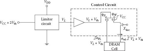
FIGURE 7.5
A voltage limiter arrangement for a DRAM cell. (Modified from “An Experimental 1 Mb DRAM with On-Chip Voltage Limiter”, K. Itoh et al., ISSCC, pp. 282–283, 1984.)
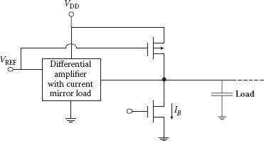
FIGURE 7.6
A typical voltage down converter. (Redrawn from “Trends in Low-Power RAM Circuit Technologies”, K. Itoh, K. Sasaki and Y. Nakagome, Proc. IEEE, Vol. 83, pp. 524–543, 1995.)
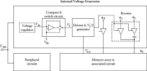
FIGURE 7.7
An internal voltage generating scheme. (Redrawn from “Dual-Operating-Voltage Scheme for a Single 5V 16 Mbit DRAM”, M. Horiguchi et al., IEEE J. Solid State Circ., Vol. 23, pp. 612–617, 1988.)
At 16 Mbit DRAM level a dual-operating-voltage scheme for a single 5 V supply was suggested in which memory array operating voltage was chosen to be 3.3 V since up to that stage of density level internal voltage converters were providing satisfactory performance. Moreover, a lower voltage <3.3 V at that stage would have required a larger storage capacitance for obtaining reliable cell signal and >3.3 V would have made excessive electric field across the memory cell capacitor [33]. Voltage converters used large standby current and dual operating-voltage was shown to be the best choice in terms of speed and reliability of the devices used; and also reduced power consumption and kept cell signal charge at a suitable level. Proposed internal voltage generator is shown in block form in Figure 7.7 along with different voltage levels. In the dual operating voltage scheme, there is an inherent problem of racing due to mismatch between memory array and peripherals. Compare-and-switch circuit is designed to overcome this problem by raising memory array operating voltage when supply voltage is considerably higher than 5 V. To achieve sufficient drivability and voltage accuracy, a driver using a simple differential amplifier with a PMOS load is found to be a suitable choice.
Because of the importance of on-chip voltage limiters, several designs, including the just discussed dual-operating voltage scheme, were reported. However, all of them had some common deficiencies like imprecise voltage regulation and effect of threshold voltage variation; both were due to variations in fabrication processes. In addition, effects of voltage bounce and feedback stability were also not attended to [31,33, 34, 35 and 36], and these internal voltage generators depended on the threshold voltage of MOSFETs (with inherent variations) [34,35], which had large dependence on the external supply voltage, operating temperature, or else depended on a band-gap reference [31,36], which used bipolar transistor on a CMOS chip, with consequential limitations including fabrication complexities. To overcome the deficiencies and some process limitations, a CMOS DRAM voltage limiter comprising a precise internal voltage generator and a stabilized driver, as shown in block form in Figure 7.8 was given by Horiguchi and others [32]. In this scheme the internal voltage generator comprising a PMOS-Vth difference generator with a voltage-up converter and fuse trimmings, was preferred. Generated voltage (|Vthp1| – |Vthp2|) maintains stability, and it is not affected because of bulk bias voltage (VBB) fluctuations which (dis) charges large bit line capacitance and is not affected by the noise of the main chip supply voltage.
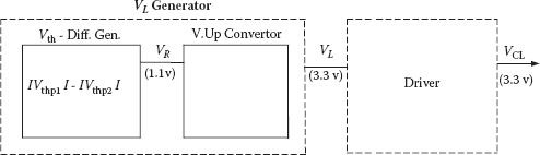
FIGURE 7.8
A voltage limiter in block schematic form. (Redrawn from “A Tunable CMOS-DRAM Voltage Limiter with Stabilized Feedback Amplifier”, M. Horiguchi et al., IEEE J. Solid State Circ., Vol. 25, no. 5, pp. 1129–1135, 1990.)
Boosted sense grounded (BSG) and negative word line (NWL) schemes are used to extend the data retention time of the DRAMs. In the BSG scheme, low level of the bit line is slightly boosted to suppress sub-threshold current of the unselected memory cell word line transistor in the active memory array. In the BSG scheme suggested by Akasura and others [37], reference voltage VREF was set at 0.5 V as shown in Figure 7.9. Large NMOS M2 turns on at the beginning of sensing, which suppresses unwanted rise in boost sense ground voltage (VBSG) due to sensing current in bit line. In the standby mode, current mirror amplifier is inactive and NMOS M3 clamps the level of VBSG. Ground line for supplying charge to the BSG line is totally separate from the global ground lines, and other circuits are not affected. The BSG scheme reduces junction leakage current helping in the increase of data retention time. However, in the BSG scheme, bit line swing becomes less than VCC which makes it a little unsuitable for low voltage operation. Negative voltage word line is another technique for the refresh time improvement [28] through the suppression of sub-threshold leakage current. As it is well known that junction leakage current under the storage node and the sub-threshold leakage current affect the refresh characteristics of the DRAMs, a small back-bias voltage VBB is used to reduce electric field between the storage node and the p-well under the memory cell. However, small VBB level reduces the threshold voltage Vth of the access transistor resulting in increased sub-threshold leakage current. Negative-voltage word line (NWL) technique suppresses the just mentioned increase of sub-threshold current. In a conventional scheme WL is controlled with VBB = −2 V; however, an improvement of 2.5-to 3-fold in the refresh time was made possible by using both VBB and low WL voltage level of −0.5 V. Since low values of Vth can be used, another advantage of the NWL technique is that is allows one to use a lower level than the conventional high level of the word lines. This suggests that even at 1.2 V, cell voltage level can be obtained in full using a boosted voltage, Vpp′ (= 2VCC), and it can be easily generated by a usual VPP generator. Figures 7.10(a) and (b) illustrate some voltage levels in conventional, BSG, and NWL schemes.
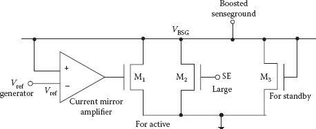
FIGURE 7.9
Circuit diagram for boosted sense-ground scheme; SE enables the beginning of sensing. (Adapted from “A 34 ns 256 Mb DRAM with Boosted Sense-Ground Scheme,” M. Akasura et al., Proc. ISSCC, pp. 140–141, 1994.)
The NWL scheme requires highly regulated and correct high levels of the word line and back-bias voltage VBB; otherwise presence of noise and/or variation in chip power supply affect access transistor threshold voltage causing serious signal loss due to increased sub-threshold current. Hence, a precise on-chip voltage generator is a necessity especially for gigabit level DRAMs. Even a 0.1 V decrease in gate source voltage of the cell access transistor increases the sub-threshold leakage current by an order. Charge pump generators shown in block form in Figure 7.11(a) are used in conventional procedure for the provision of high and low WL voltages in a DRAM. The output generally has a ripple of nearly 0.2 V, which is reduced by combining series pass regulator with charge pump regulator as shown in Figure 7.11(b). The series pass regulators need accurate WL offset voltages, which are made available by combining band gap reference with a differential amplifier and current mirror offset voltage generator, where accurate offset voltages were produced using mirror current as illustrated in ref. [39]. Band gap reference voltage generator can be selected among many available circuits; however, one MOSFET is preferred over a BiCMOS for high-density DRAMs.
It is well established that on-chip supply voltage conversion has become essential and a number of schemes are available. However these conventional methods used as much as half to two-thirds of total chip power at 1 Gbit/4 Gbit DRAMs. As an alternative, two internal circuits were connected in series between supply rails [38]. Both the internal circuits had identical DRAMs with same core and peripherals except input/output buffers and both circuits operated with the same clock. As a result, the AC current waveform in both circuits was the same and more importantly voltage across each DRAM was fixed at VDD/2 without using any conversion process. The technique was successfully tested using two 4 Mbit DRAMs.
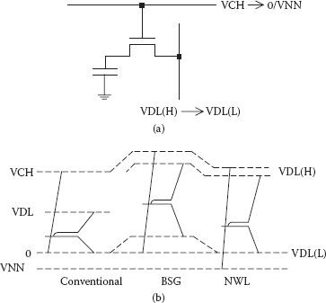
FIGURE 7.10
(a) Basic cell, and (b) voltage levels, in conventional, BSG, and NWL schemes. (Adapted from “A Precise On-Chip Voltage Generator for a Giga-Scale DRAM with a Negative Word-Line Scheme”, H. Tanaka et al., Symp. VLSI Circ. Dig. Tech. Papers, pp. 94–95, 1998.)
Substrate requires enough negative bias when chip is active. Obviously power dissipation of the bias generator should be low, and it should be able to provide adequate voltage level at greater efficiency. As the working voltage of the DRAM chip decreases, back-bias voltage level also has to go down; its value (range) is decided based on the following. Back-bias voltage (VBB) level depends on the value of the threshold voltage of the access transistor in the DRAM whose upper and lower limits are decided by the boosted word line voltage and suppression of the sub-threshold leakage current, respectively. For the upper limit, the word line voltage needs to be (VCC + 1.2 Vth), where Vth is the increased threshold voltage of the access transistor with its source at VCC level. [40]; effective back-bias voltage becomes (VCC + |VBB|). For a practically available word line voltage of ~1.7 VCC′ an upper limit of Vth is 0.88 V at VCC = 1.5 V. As mentioned, the sub-threshold leakage current decides the minimum required value of the threshold voltage. The accepted value of memory cell capacitance of 30 fF (~25 fF has also been considered safe by a large number of reports) and the data hold time of 100 ms, Vtho (with source connected to ground) should be larger than 0.6 V for keeping sub-threshold leakage current less than 11 fA per cell. It requires that VBB of lower than −1.0 V is essential in a 1.5 V DRAM [40].
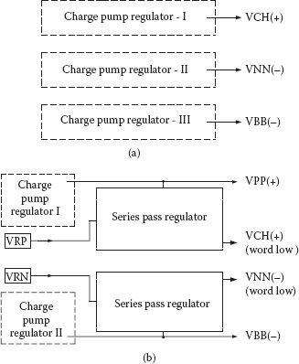
FIGURE 7.11
Schematic of a voltage regulator for negative word line scheme. (a) Charge pump regulator (conventional), and (b) hybrid regulator. (Adapted from “A Precise On-Chip Voltage Generator for a Giga-Scale DRAM with a Negative Word-Line Scheme”, H. Tanaka et al., Symp. VLSI Circ. Dig. Tech. Papers, pp. 94–95, 1998.)
Few circuits are available for on-chip back-bias generation. Figures 7.12(a) and (b) show a conventional pumping circuit (CPC) and hybrid pumping circuit (HPC), respectively [40]. In CPC, which uses two PMOSs, the VBB could not be pumped lower than |Vthp| – VCC, whereas in HPC it could reach (–VCC). Working of the HPC can be understood by following the clock when it is low and then high. When CLK is low, node voltage N5 is clamped to ground level. When CLK changes to high, node N4 rises to |Vthp| and by capacitive coupling node N5 voltage level and VBB become −VCC. In HPC no threshold voltage is lost while generating VBB. An important precaution for the HPC is that the NMOS used in the pumping circuit needs to be fabricated in a triple-well structure to avoid the minority carrier injection, which could destroy stored data.
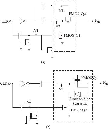
FIGURE 7.12
Back-bias generator: (a) conventional circuit, and (b) hybrid pumping circuit (HPC). (“An Efficient Back-Bias Generator with Hybrid Pumping Circuit for 1.5V DRAMs”, Y. Tsukikawa, el.al., Symp. VLSI Circ. Dig. Tech. Papers, pp. 85–86, 1993.)
7.7.2 Voltage Limiting Schemes
On-chip voltage limiters are extremely important for reducing DRAM power dissipation and the enhancement of device reliability. Utility of the voltage limiter is considerably improved when it also generates precise voltage during burn-in and stress conditions are applied automatically. A DRAM voltage limiter with a burn-in test mode was given by Horiguchi and others as shown in Figure 7.13(a) [41]. It is based on the simple arrangement where the DRAM core (circuit L1) operates on the internally generated voltage VL, and the peripherals (circuit L2) and the voltage limiter operate on the external supply voltage VDD. In a burn-in test VL and VDD are raised and a number of schemes are available; however, these have focused mainly on voltage stability under normal operation [41]. A dual-regulator dual-trimmer scheme shown in Figure 7.13(a) is one such practical scheme in which not only a precise high voltage for burn-in test is available, but it also maintains a constant limited voltage under normal condition. Here the compare and switch outputs exceed the two regulated and trimmed voltages VRN and VRS. The regulator EB keeps (VDD – VRB) constant, independent of temperature—an important condition for proper circuit operation. Accurate burn-in voltage is obtained by simply raising VDD. In addition, the two sets of trimmers TB and TN reduce any deviations in the generated voltage due to the process variations, especially the change in threshold voltage Vth. Circuit realization of VRB regulator and VRN regulators used biasing circuit which employed PMOS threshold voltage difference scheme; otherwise any other suitable circuit can also be used. Each trimmer block comprises a differential amplifier, an output transistor, and a variable negative feedback circuit (FB or FN), some details of which are shown in Figure 7.13(b). Deviations in burn-in voltage as well as in the normal operating voltage were reduced to ± 0.13 V while using only six fuse ROMs. Main limitation of the reference generator is the use of 100–1000 kΩ resistors and large amount of standby current because of the presence of quite a few differential amplifiers and DC current paths in the voltage divider, making it unsuitable for low power battery-operated DRAMs. A dynamic reference voltage generator that consumes considerably less current has been proposed, as shown in Figure 7.14 [42]. Threshold voltage difference ΔVth and resistance RR determine the reference current IR, which is mirrored to the output node and flows through RL, and output voltage depends only on ΔVth and resistance ratio. Hence, accurate output voltage is available even when ΔVth may vary due to fabrication process limitations, as polysilicon fuses accurately trim the resistance RR. In the experimental verification, pulse widths of φ1 and φ2 were taken as 200 ns and 100 ns, respectively, and the generator current could be reduced to less than 1 μA, making it suitable for battery-operated DRAMs [42].
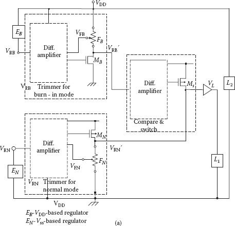
FIGURE 7.13
Voltage limiter with symmetrical dual trimmers using decoding scheme having (a) trimmers and compare-switch circuit, and (b) details of negative feedback circuit. (Redrawn from “Dual-Regilator Dual-Decoding-Trimmer DRAM Voltage Limiter for Burn-in Test”, M. Horiguchi et al., IEEE J. Solid State Circ., Vol. 26, pp. 1544–1549, 1991.)
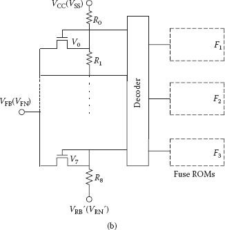
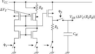
FIGURE 7.14
A dynamic reference voltage generator. (Modified from H. Tanaka et al., “Sub-1-μA Dynamic Reference Voltage Generator for Battery-Operated DRAM”, Symp. VLSI Circ. Dig. Tech. Papers, pp. 87–88, 1993.)
Improvement of DRAM cell retention time is a critical factor in realizing high-density DRAMs, since it needs to be doubled with every generation and chances of failure of weak cells rise. At the same time the main source of trouble is that leakage currents continue to grow with reduction in minimum feature size. Several approaches have been followed for successful extension in refresh time. Reduction in leakage currents is very important in this direction and is a matter of discussion in Section 7.7. Another kind of scheme depended on the knowledge that data retention capability of the cell depended on operating temperature and voltage, and random variations in parameters which are inherent in fabrication processes. Quite a few schemes were given which tried to set optimum internal refresh periods by using temperature detectors [43,44,45] and internal voltage converters [45], or through measuring voltage degradation of weak cells [46]; however, DRAM design had to continue to improve their speed, which resulted in increased power dissipation as well. At the same time, the JEDEC standards adopted an extended temperature range of (85 to 95°C) from the earlier temperature range of 0 to 85°C, and it is now operating in servers [47,48]. DRAM data retention time became half of that in this extended temperature range compared to the standard temperature range, which was 64 ms. Corresponding to 64 ms refresh interval (tREFI), the interval at which refresh command must be sent to each DRAM (from an internal counter to the next part of the chip as per JEDEC standard) was 7.8 μs (64 ms divided by number of rows) for 256 Mbit DDR2 DRAM. DRAM density requires doubling of refresh time (tREF) with every generation using conventional methods. The problem was circumvented in some cases by doing simultaneous refreshing of a number of rows with single command [49], but it requires larger charging current and hence delay in terms of refresh cycle time (tRFC), the amount of time that each refresh takes. For the current in-use DDR3 4 Gbit DRAM, it requires tRFC of 300 ns, and it may go to 350 ns for 8 Gbit [50].
Error control codes have also been used to minimize errors along with conventional techniques for refresh time extension. The combination of longer refresh time along with shorter refresh time for a few rows has also been used [51,52]. The major drawback of all such approaches was that multiple refreshing was done on a row basis and with cumbersome measurement methods. Probably, the main reason was the failure to identify the weak cell efficiently and develop a systematic approach. A multiple refresh scheme in terms of an algorithm, which depended on error correction, was also proposed for optimal selection of multiple refreshing periods [53]. Boosted sense ground (BSG) schemes discussed in Section 7.7 have been effectively used to double the refresh period [37].
Instead of a row-based refreshing method, a novel method of refreshing on a block basis was given in which a large number of multiple refresh periods match the required refresh period of the blocks as closely as possible [54]. Consider a 16-cell memory as shown in Figure 7.15(a) where data retention time of each cell is written in each square (cell). In conventional refreshing tREF must not exceed the minimum retention time of all cells, that is, 2. If the array of Figure 7.15(a) is broken into a 4 cell block as shown in Figure 7.15(b) then four different refreshing periods can be used; 8 for row 1, 2 for rows 2 and 4, and 6 for row 3. If the array is further divided in blocks of two cells as shown in Figure 7.15(c), blocks may be refreshed with tREF of 2, 4, 6, 7, 8, 9, 12, and 15. DRAM architecture of the block-based multiple period is also made available for the purpose of generation of refresh signal, bit selection, and multiple period refreshing. A polynomial time algorithm is provided that computes set of optimal refresh periods for the selected blocks. As the selected blocks comprise cells having closely valued tREF, these refresh periods are obtained during post-fabrication testing of memory array. Moreover, the method needs nearly 6% chip area overhead and was not tested at higher operating temperature.
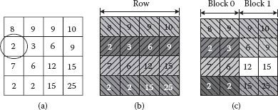
FIGURE 7.15
Memory with 16 cells: (a) data retention times, (b) necessary refresh period using blocks with 4-cell, and (c) 2-cells. (Redrawn from “Block-Based Multiperiod Dynamic Memory Design for Low Data-Retention Power”, J. Kim and M. Papaefthymiou, IEEE Trans. on VLSI Systems, pp. 1006–1018, 2003.)
The JEDEC DDRx standards have allowed for spacing in refresh operations. If a small number of tREF periods are delayed, data are not lost provided that all cells have been refreshed satisfactorily. This deferral of refresh count is eight for the DDR3 standard [55]. A memory controller receives read and write instructions from the CPU and places in the input queue and then moves to an available space. The memory controller also has to execute refresh operation. The selection between various operations including refreshing is done by the memory scheduler. A significant report has investigated for optimum priority scheduling read/write and refresh [55]. Scheduling of refresh command has not been used often. Usually the refresh scheduling algorithm asked for refresh operation as soon as tREF period expired as tRFC was not affected much, and at the same time it required simple hardware logic control. In a much better scheme, which has been given the name defer until empty (DUE), refresh operations are not selected over read/write until refresh deferral count reaches seven refresh operations. However, even these kinds of designs are not good enough in containing refresh penalties. For example, take the case of low-multilevel parallelism (MLP) workloads. There are many time slots when the memory controller bank queues are empty but refresh scheduler will continue to provide refreshing when tREF counter expires; along with long tRFC, it results in large penalties by the memory controller. Even with high DRAM bus utilization refresh penalties accrue due to scheduler inefficiencies [55]. The elastic refresh algorithm has been proposed, which betters the other schemes including the DUE approach, in which an additional period of time is added for waiting for the rank to remain idle before the refresh command is given. A detailed study was undertaken for evaluating the elastic refresh scheme and was compared with best-known algorithm DUE.
The temperature and supply voltage dependence of tREF and the identification of weaker cells are helpful in devising a mechanism of extending refreshing duration. An important study has shown another cause on which tREF depends. For analysis purposes, three chips were fabricated in 54 nm technology with different types of cell structures like recessed and buried word line, and variation of tREF was studied for different data patterns like all cell high and all cells low with only one cell high. It was observed that tREF is determined not only by the cell leakage but also by the bit line sense amplifier (BL SA) offset. As data patterns determine the interference between bit line and word line, this also affects tREF. Dependence of tREF on data patterns is found by studying relation between cell leakage characteristics and its own offset variation [56]. The chip having smallest variation in tREF shows the best offset variation and the worst leakage, whereas the chip having largest variation in tREF shows the best cell leakage characteristics. The study concluded that it is only important to improve the BL SA offset present due to data patterns, and it will reduce tREF variation.
7.9 Sub-Threshold Current Reduction
Sub-threshold current in an NMOS is given as
(7.9) |
where Vtho is the threshold voltage when source and bulk substrate are at same potential, and γ is the body effect coefficient. VGS, VBS, and VDS are the respective device terminal voltages, λ is the drain-induced barrier lowering (DIBL) factor, k is the Boltzmann constant, T is the absolute temperature, and q is the electron charge. Here, Is is the drain current coefficient, and n is the sub-threshold swing parameter, which is related with slope factor S, a quality metric of sub-threshold region as to how much reduction in VGS produces an order of magnitude reduction in the sub-threshold current. It is given as
(7.10) |
where CD is the depletion layer capacitance, and Ci is the insulator capacitance of the MOSFET.
In low-voltage DRAMs, if threshold voltage Vth is also scaled down (though not in proportion to the supply voltage), it will result in increased Isub. The most effective way of overcoming this problem of increased Isub is to keep Vth high as before in the DRAM cells and peripheral circuits, both in the active mode and in the standby mode. Depending upon the DRAM topology and its circuit operation, the importance of reducing Isub in different modules varies and shall be discussed accordingly. During fabrication, value of Vth is increased mostly by increasing the doping level of the MOSFET substrate, but application of reverse bias(es) is the most effective way even after fabrication and it can easily be applied to only the selected low Vth MOSFET circuits. Idea of affecting Isub through device terminal voltage reverse biasing is obvious from Equation (7.9) and almost all suggested techniques fall in this broad category. A fine description of the classification of reverse biasing techniques and the respective leakage reduction efficiencies is available in ref. [8].
As mentioned earlier, Isub has to be reduced in the DRAM core, and in the peripheral circuits in the active and sleep modes. Different techniques are available, some of which are specific for active or for sleep mode and some are applicable in general. For better understanding, Section 7.10 describes only those techniques which are better suited for peripheral circuits.
7.10 Multithreshold Voltage CMOS Schemes
Multithreshold voltage CMOS technology scheme (MTCMOS) proposed by Mutoh and others not only reduces standby current, but it also obtains high-speed performance at low supply voltage using low threshold MOSFETs [57]. Figure 7.16 shows basic MTCMOS scheme in which all logic gates use low Vth (0.2–0.3 V) MOSFETs, and its terminals are not directly connected to supply rails but to virtual supply rails. High threshold (0.5–0.6 V) MOSFETs M1 and M2 link the actual and virtual power lines, and they act as sleep mode control transistors through select signals SL and . Sleep control transistors are relatively wider with low on-resistance value; hence, when asserted, virtual supply lines function as real. However, larger I sub of low-Vth logic is almost completely suppressed by M1 and M2 having large Vth. Performance of the MTCMOS circuit depends on the size of the control transistors and the capacitances of the virtual power supply lines. Voltage deviations in supply lines due to the switching of the logic gates are suppressed by having larger values of supply line capacitances. It is claimed that MTCMOS operates almost as fast as low V th logic and at supply voltage of 1.0 V its delay time is nearly 70% less than that for the conventional logic gate with normally high Vth.
FIGURE 7.16
Basics of an MTCMOS scheme. (“1-V Power Supply High-Speed Digital Circuit Technology wth Multithreshold-Voltage CMOS”, S. Mutoh et al., IEEE J. Solid-State Circuits, Vol. 30, pp. 847–854, 1995.)
FIGURE 7.17
(a) MTCMOS latch circuit, and (b) problematic leakage current path.
Since latches and flip-flops are memory elements and should retain their data even in sleep mode they need special attention in MTCMOS. An MTCMOS latch circuit is shown in Figure 7.17(a); it has conventional inverters Ib and Ic, which have high Vth and are connected directly to the actual supply rails. Data is retained by the latch even in sleep mode because the latch path consisting of inverters Ib and Ic continues to receives power. Inverter Ia and the transmission gate TG (both with low Vth MOSFETs) form the forward path and provide high-speed operation. In this path, control transistor M1 and M2 (high Vth) are also included for maintaining proper operation which is better understood through Figure 7.17(b). Since node N1 shall be in low state during sleep mode, real and virtual rails would be connected through on PMOS transistors Map and Map′, thereby increasing current in the sleep mode. Therefore, inclusion of the control transistors M1 and M2 becomes essential.
The MTCMOS circuit technique is an excellent method so that logic can work at low voltage, however, use of high Vth MOSFETs in the critical path for holding data creates bottlenecks. So, special circuits called balloon circuits have been used which help in preserving the state of nodes even during the sleep mode, without having high Vth MOSFETs in the critical paths [58]. The balloon circuit, as shown in Figure 7.18(a), is connected to the real supply directly, but it does not operate in the active period; hence, there is no requirement on its speed. Balloon circuits are therefore realized with normal high Vth, minimum size MOSFETs with low standby power, and chip area penalty. Signals B1 and B2, as shown in Figure 7.18(b), control the transmission gates (TGs), and their states decide the active mode or sleep mode period. In the active mode, node A does not float because leakage current of the low Vth TG flows and the balloon is not in the critical path, which avoids the bottleneck of the earlier MTCMOS technique.

FIGURE 7.18
(a) Typical balloon circuit and (b) sleep operation of the balloon circuit. (Modified from “A 1-V high-speed MTCMOS circuit scheme for power-down applications”, S. Shigematsu et al., Symp. VLSI Circuit, Dig. Tech. Papers, pp. 125–126, 1995.)
Use of balloon circuits improves the operation of MTCMOS circuits; however, it costs chip area and needs a timing control scheme for switching of operating modes. Another data holding circuit is proposed that uses intermittent power supply (IPS) scheme with low Vth transistors without any increase of leakage currents [59]. In this scheme, virtual power lines are cut off from the mains and connected only intermittently during sleep mode; hence, no extra state holding circuit is required. In an experimental latch, fabricated in 0.35 μm CMOS technology, saving of 30% chip area, 10% reduction in delay, and 10% reduction in active power consumption were obtained in comparison to the conventional MTCMOS case.
For battery-based application, along with performance (speed), energy consumption is critical. Hence while developing a dual Vth MOSFET process at 0.18 μm level, energy-delay product (EDP) was extracted from measured data. Investigations done with VDD and Vth variations gave following important inferences: (1) for minimum EDP, optimum (Vth/VDD) ~ (120 mV/300 mV), (2) optimum Vth is a logarithmic function of the activity factor of the application, and (3) dual Vth process gives good results with high sleep mode durations operation cases [60].
In general, leakage-sensitive circuits like dynamic NOR gates, which require level keeper for compensating loss of charge, are not preferred in DRAMs [61]. However decoders of modern CMOS DRAMs do use dynamic NAND gates for rows. With technology at 0.1 μm and beyond, use of dynamic circuit was bound to increase, even when dynamic circuits are significantly worse in terms of Isub in comparison to the static circuits. Consequently, low Vth devices, as normally used in static MTCMOS circuits, cannot be used for reducing delay in critical paths. In spite of the limitation, dynamic circuits became a necessity in high-speed submicron process technologies as they were faster by at least 25% in comparison to the static counterparts [62]. A study at 0.25 μm technology optimized for 1.8 V VDD observed that in dynamic circuits with Vth > 300 mV, Isub can be maintained at an acceptable level of nearly 1 nA/μm (at 30°C), but for Vth < 300 mV, Isub is substantially higher than 1 nA/μm, and it is independent of channel length. Moreover, Isub multiplies steeply with rise in working temperature and a functionality problem is created in dynamic circuits. A solution was proposed that dynamic substrate bias be used to raise the threshold voltage in standby mode, which would reduce Isub several orders of magnitude. Performance is not degraded since source-to-well reverse bias is not applied in active mode, retaining low values for Vth [62].
A high Vth significantly reduces Isub of a MOSFET; however, it also results in its higher equivalent on-resistance deteriorating propagation delay. Empirically, Vth is kept around 20% of VDD supply voltage for proper maintenance of balance in Isub and propagation delay [63], but for low voltage DRAMs, Vth (20% of VDD) becomes too small. The problem has been minimized by using varieties of circuits with dual-threshold MOSFETs. In one such scheme, low Vth devices are used in critical path(s) for achieving high performance, with the lower limiting value of Vth depending on noise margin, whereas high Vth devices are used in noncritical paths and the value of the Vth may range between low Vth to 0.5 VDD. However, a major concern is in the distinction and selection of paths that would use higher Vth devices, as it may convert some of the noncritical paths to critical ones; it also depends heavily on the value of higher Vth used. If the value of higher Vth is slightly more than low Vth, a large number of MOSFETs can be assigned this value without turning the path into critical one but improvement in Isub shall be small. On the contrary, with too large a Vth, only few paths can use such devices, though with improved Isub. Therefore, it needs a solution for optimum value of Vth, and a levelization back-tracing algorithm is one such attempt which selects and assigns optimal high-Vth [64]. The algorithm begins with initializing a circuit with one value of low Vth, then high Vth is assigned to some devices lying in noncritical paths (within the constraints of certain performance limits). This assignment is done by “back-tracing of the slack of each node level by level.” Here slack means possible slowdown of a gate without affecting the overall performance of the circuit. The value of Vth is increased till such time that slack becomes zero. Use of the algorithm on certain ISCAS benchmark circuits has shown reduction in active and standby leakage power even up to 80% [64].
7.10.1 Stacking Effect and Leakage Reduction
Insertion of an extra transistor between the supply line and the pull-up transistor of driver circuit was shown to create a reverse-bias between gate and source of the driver transistor when both transistors were off [58]. Result was a substantial decrease in Isub and this phenomenon is referred to as the stacking effect. For a more general case a transistor stack of arbitrary height was studied, taking into account the body effect as well as drain-induced barrier lowering factor (DIBL), which also becomes significant for submicron devices [65]. It was observed that the leakage power also depended on primary gate-input combination. In another model for the stack effect, a stack effect factor, ratio of the leakage current in one off device to that for a stack of two off-devices, was found to be dependent on the process parameters, sub-threshold swing S, and the power supply voltage VDD [66]. The stack effect reduction factor was shown to increase with downward technology scaling, which was basically due to expected increase in DIBL factor λd and possible reduction in supply voltage. Stacking of devices does reduce Isub, but drive current of a forced stack is lowered, resulting in increased propagation delay. It suggests that stack forcing would be used in noncritical paths, similar to the dual Vth scheme. Of course there can be a delay leakage trade-off and paths which are faster than as per local requirement can be slowed down with a condition that such slow down does not affect the overall performance. The forced stack technique, which effectively reduces Isub of noncritical paths, can be used with and without the dual Vth process. Common gates like NAND, NOR, or more complex ones do have stacked gates in their original form. During standby, if numbers of stack devices are off, Isub can be reduced. However, it is not practical to have all stacked devices off throughout the time duration of sleep mode. In case, if stacking is forced in both n-and p-networks of a gate, leakage will surely be reduced, irrespective of the input logic levels [66].
Analysis of the scaling of stack effect and improvement in gate leakage also showed possibility of performance degradation and required sleep mode input vectors to take full advantage of stacking. An enhanced MTCMOS scheme is also available, as shown in Figure 7.19 with stack transistors M1 and M2 placed between low Vth logic and the ground for leakage control in standby mode [67]. This scheme has an important characteristic of eliminating the need of input vector set for minimizing leakage current and works on a single sleep-mode signal S for turning off both the transistors in the sleep mode. It has been shown that optimum stack height is only two, but at the same time, the size of the two MOSFETs is to be optimized, which will minimize performance degradation and leakage power consumption [67]. Since the method of optimization given here took into account only sub-threshold leakage in standby mode and not the gate leakage, a better proposition takes into account the increasing gate leakage, which is expected to be a dominant component in total leakage [68,69]. At the same time it is also important to consider leakage power drawn in the active mode, during such optimization.
FIGURE 7.19
Enhanced MTCMOS scheme with stacked sleep devices for leakage reduction. (Modified from “Analysis and Optimization of Enhanced MTCMOS Scheme”, R.M. Rao, J.F. Burns and R.B. Brown, Proc. 17th International Conf. VLSI Design (VLSID’04), 2004.)
For the forced stacking scheme, it was shown in ref. [70] that to ensure same performance as that of a conventional MTCMOS scheme with one MOSFET of width W inserted between logic and ground, sizing of the MOSFETs of Figure 7.19 (W1 and W2) must be done according to the following relation and constraint:
(7.11) |
Though the device sizes optimize sub-threshold leakage, there is always an increase in the gate leakage current if identical performance is a constraint as mentioned above, and for optimizing total gate leakage, including Isub, size of the upper device M2 must be smaller than that of M1; unfortunately, it is a contradictory condition for Isub optimization. For a circuit with smaller active duration than sleep-mode, input occurrence probability is also small and if the circuit is optimized in terms of total leakage saving, it will give more benefit than a case when it is optimized in terms of sub-threshold leakage only. Hence, it is always better to optimize for total leakage [55].
The sleepy stack leakage reduction technique suggests a structure which combines previously discussed sleep transistor technique and the forced stack technique to achieve up to two orders of leakage power reduction in comparison to the forced stack. It also retains the original state unlike the sleep transistor approach, though the advantages come at a small price of some chip area and delay cost.
Figure 7.20 shows a sleep transistor inverter which isolates the existing logic network whereas in the forced stack transistor inverter, existing transistor is broken into two to take advantage of stacking. In the sleep stack mode existing transistors are divided into two with each one being half the size of the original transistor width [71]. During active mode, as shown in the figure, all sleep transistors are turned on to switch faster than the forced stack structure. In addition high Vth transistor and its parallel transistor may be used for the sleep transistor. In the sleep mode both the sleep transistors are turned off, keeping the sleepy stack structure its original logic. Leakage current is reduced by high Vth sleep transistor/parallel transistors and in addition stacked and turned-off transistors produce stack effect with further reduction in leakage current. Combined effect of the above achieves extremely low leakage power consumption while retaining the original logic.
FIGURE 7.20
Sleepy stack inverter showing W/L of each transistor in active mode assertion, and sleep mode assertion. (Redrawn from “Sleepy Stack Leakage Reduction”, J.C. Park and V.J. Mooney, IEEE Trans. VLSI Systems, Vol. 14, pp. 1250–1263, 2006.)
7.10.3 Importance of Transistor Sizing
Circuit designers would like to size the NMOS sleep transistor large enough for achieving a good performance. Virtual ground is preferred to be as close to the actual ground as possible, which would force drain-to-source voltage of the high-Vth sleep transistor to a small value so that it is biased in the linear region, enabling it to be represented by a linear resistor. However, if the sleep transistor is sized too large, not only the chip area shall be wasted, energy overheads during sleep-active mode switching would increase; whereas the circuit becomes slow during high-to-low transition if the NMOS transistor size is too small because of the increase of its resistance. Hence, deciding the optimum size of the sleep transistor needs further analysis. At first, let us consider the effect of its on-resistance Rs, on with the assumption that parasitic capacitance Cs,on as shown in Figure 7.21 is negligible. A voltage drop developed across Rs′on during any charge flow from low-Vth logic will affect the working of the MTCMOS scheme. It will reduce the drive of the logic transistor from VDD to VDD – VVG′, and because of the raised potential of the source of pull-down logic NMOS transistors, their threshold voltage would increase; both the effects increase high-to-low transition time tpHL. With the continued downscaling of supply voltage and almost constant Vth, effective Rs′on of the sleep transistor is bound to increase and to keep it at the same level (if not able to reduce it), another large size device is to be used. In addition for increasing its drive, overdriving of the sleep transistor gate can also be used.
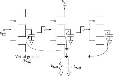
FIGURE 7.21
MTCMOS block illustrating equivalent resistance, capacitance, and reverse conduction effects. (“Dual-Threshold Voltage Techniques for Low-Power Digital Circuits”, J.T. Kao and A.P. Chandrakasan, IEEE J. Solid-State Cir., Vol. 35, pp. 1009–1018, July 2000.)
The parasitic capacitance shown in Figure 7.21, caused by wiring and junction capacitances serves as local charge sink (and source) and reduces transient spikes in the circuit while switching between sleep and active modes. But Cs,on is not able to reduce the effect of the IR drop of Rs,on unless it becomes too large, which is not desirable; hence, proper sizing of the sleep transistor is very important [72]. As shown in Figure 7.21, there are some other problems as well. For example, when the current flows backward through the low Vth NMOS from the virtual ground and charges up the output capacitance for PMOS sleep transistor, its output is raised from zero to VVG′ and a PMOS with low input might experience a reverse conduction [72]. This charging current gets accumulated while other gates discharge from high to low and only a small portion of this current flows through the sleep transistor. Consequently, MTCMOS structure becomes a bit faster as voltage drop across the sleep transistor shall be a little less than if all the current would have flown through it. Another effect of the reverse conduction is to precharge the output to VVG instead of its original value of 0 V and required charging effort from low to high becomes a little less, thus lowering tpLH. On the flip side, noise margins are reducing, which in worst cases may lead to malfunctioning.
Optimum sizing of sleep transistor becomes increasingly difficult in complex MTCMOS circuits because critical paths, depending upon the input-vectors in a basic CMOS circuit, do not translate into critical circuits in MTCMOS. Exhaustive simulation of the complete circuit for all combination of inputs needs to be done with the sleep transistor’s size as a variable parameter. To avoid this cumbersome process, a suggested alternative for optimal transistor sizing is based on mutual exclusive discharge pattern [73], which ensures the performance of a complex MTCMOS circuits within prescribed performance limits for all possible input patterns. In this procedure, at first it is ensured that individual gates are allowed to be degraded by only a fixed percentage, which guarantees that a complex MTCMOS constructed from these gates shall not degrade by more than the same limit from its original CMOS version. While implementing this method, it is not necessary to determine worst case input vector for the whole circuit, which makes it an easier alternative. An individual gate is exhaustively simulated to determine its own high-Vth sleep transistor, then these sleep transistors are merged as they can be shared among mutual exclusive gates [72]; the gates do not discharge at the same time. Through merging of sleep transistors, important chip area is saved. An algorithm has been developed and shown to work on LSI logic for transistor sizing and merging for fixed percentage of performance degradation [74].
In MTCMOS circuits, high Vth series sleep transistor always degrades performance while reducing the leakage power consumption. An alternate to it is dual-Vth domino logic where already existing devices in the logic are assigned high and low Vth; hence, an extra sleep transistor is not needed. Dual Vth domino style has the sleeping mode leakage consumption of a purely high-Vth logic, but performance is decided by the low-Vth devices. It happens because of the fixed transition directions in domino logic, which allows using the dual-Vth domino gate with low leakage, and high Vth devices are used in noncritical paths without affecting performance [75]. Dual-Vth domino logic does not have to do the device sizing and at the same time performance degradation due to series sleep transistor is also avoided.
Peripherals of DRAM contain a large number of logic circuits, like decoders, word drivers, and column drivers, and these circuits are in multiple numbers. Isub of these drivers/circuits becomes substantial as their total width becomes more than widths of transistors on the rest of the chip and threshold voltage of the driver transistors is also necessarily low for obtaining high speed. Therefore, reduction of Isub for these circuits assumes significant importance.
In a conventional CMOS driver, either NMOS or PMOS is off during steady-state condition. However, even for VGS = 0, small threshold current flows in the off MOSFET with its gate under weak inversion. Expression of the Isub under this condition is given as
(7.12) |
When the threshold voltage is reduced from −Vth1 to −Vth2, leakage sub-threshold current at VGS = 0, increases from Isub1 to Isub2 for a PMOS as shown in Figure 7.22, which results in larger power consumption in the standby mode of the MOSFETs. One of the most effective ways to minimize the increase in Isub is to have a circuit arrangement in which VGS is increased automatically either by lowering the source voltage or increasing the gate voltages and Isub2 can be reduced to Isub1 if VGS reversed by ΔVGS as shown in the figure.
Basic scheme for self-reverse biasing is shown in Figure 7.23 wherein a low-Vth PMOS, MSP is inserted between the common source of PMOS transistors MP1 to MPn of the drivers and the power supply VDD. The inserted PMOS turns on during active mode and switches off in the standby mode [76,77]. Since, in the decoded drivers, the same kind of circuits are arranged repeatedly, but only a few (or even one) operate, the width of the transistor MSP is barely sufficient to provide on current to only a few active drivers. In the standby mode, gate NMOSs are turned on and PMOSs off, and the switching PMOS-MSP is also turned off. Therefore, the large sub-threshold current of all the drivers is reduced to a small value, which is the sub-threshold current of the MSP only, because of its automatic reverse bias to MP. This reverse biasing is due to the stacking effect of MSP working like a power switch and providing source impedance to MP. It is important to note that reverse biasing and hence Isub are controllable with the threshold voltage Vths and channel width WSP of the inserted PMOS. Larger reverse biasing can completely cut off the switch but recovery time from sleep mode to active mode becomes large and creates spike noise, whereas smaller reverse biasing allows some leakage flow, but problems are reduced [77]. Generally, a low Vths MOS is preferred as it also improves its trans-conductance and drivability with smaller channel width.
FIGURE 7.22
Transfer from state A to state B due to lowering of the threshold voltage from Vth1 to Vth2. (Redrawn from “Sub-threshold Current Reduction for Decoded-Driver by Self-Reverse Blasing”, T. Kawahara et al., IEEE J. Solid State Circuits, Vol. 28, pp. 1136–1143, 1993.)
FIGURE 7.23
Sub-threshold-current reduction by self-reverse biasing through decoded-driver. (Redrawn from “Sub-threshold Current Reduction for Decoded-Driver by Self-Reverse Blasing”, T. Kawahara et al., IEEE J. Solid State Circuits, Vol. 28, pp. 1136–1143, 1993.)
Basics of offset gate driving indicate where the input voltage is overdriven. Since the logic swing of the output is smaller than the input, the technique is slightly difficult to be applied to random logic, but it has been applied for reducing leakage current in bus drivers, as shown in Figure 7.24 [78], in power switches having low actual Vth [79] and in RAM cells [80,28]. The bus driver in Figure 7.24 is a conventional CMOS inverter with low Vth, but supply lines are VDL and VSL; hence, its output voltage swing is reduced, making it faster than a conventional inverter with normal supply VDD. For proper operation of the scheme, a bus receiver is also required which converts reduced voltage swing of bus to full voltage swing for the logic. Power dissipation can be reduced up to two thirds compared to conventional architecture.
Logic circuits can be operated in 0.5 V–0.8 V VDD range, provided Vth is in the range of 0.1–0.2 V. Super cutoff CMOS (SCCMOS) scheme has been proposed which overcomes the problem of high leakage in standby mode with small value of Vth; [79]. Figure 7.25 shows the basic scheme of SCCMOS in which a low-Vth (0.1–0.2 V) cutoff PMOS is inserted in series with the logic circuits consisting of low-Vth MOSFETs. Gate voltage (VG) of M1 is at ground level when logic is in the active mode and in the standby mode VG is over-driven to VDD + 0.4 V for completely cutting off the leakage current. In a test chip fabricated with 0.3 μm triple-metal CMOS technology, working on 0.5 V VDD, standby current per logic gate could be reduced to 1 pA. However, problems mentioned in connection with a perfect switch remain present. Negative word line technique described in Section 7.7 to suppress the increase in Isub due to shallow VBB is another example of offset gate driving.
FIGURE 7.24
Concept of offset driving applied to a BUS, with VDL < VDD and VSL > VSS. (Modified from “Sub-1-V Swing Bus Architecture for Future Low Power VLSIs”, Y. Nakagome et al., Symp. VLSI Circuits, Dig. Tech. Papers, pp. 82–83, 1992.)
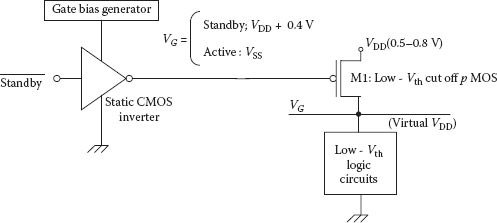
FIGURE 7.25
Concept of super cutoff CMOS through pMOS insertion. (Redrawn from “A Super Cut-Off CMOS (SCCMOS) Scheme for 0.5V Supply Voltage with Picoampere Stand-by Current”, H. Kawaguchi, K. Nose and T. Sakurai, IEEE J. Solid-State Circuits, Vol. 35, pp. 1498–1501, 2000.)
For high-speed and low-power operation, both supply voltage VDD and threshold voltage Vth can be lowered. The problem of higher leakage current can also be solved by applying a substrate bias during standby mode, which increases the threshold voltage. However, in the active mode, the substrate bias is not applied, retaining low Vth and higher performance.
In a test DRAM, fabricated in 0.3 μm technology, Vth could be increased to 0.7 V from 0.3 V by applying a substrate voltage of −2 V. Basic scheme of such a standby power reduction is shown in Figure 7.26, consisting of a level-shifter and a voltage switch. During active mode n-well bias mode VNWELL = VDD = 2 V and p-well bias VPWELL = VSS, whereas during standby mode respective values are set at 4.0 V and 2 V. Standby to active mode transition and vice versa takes about 50 ns [80]. Substrate biasing technology has successfully been used in the fabrication of processors [81,82] and for the reduction of leakage in power switches [83].
Offset source driving is similar to the VGS reverse biasing scheme to the extent that it also uses source switches, but its behavior is considerably different as the input gate voltage and output drain voltage are not up to full swing and the source terminal voltage is also not at VDD or VSS. This makes a huge difference with the leakage current reduction efficiency. Control of the MOS transistor source voltage is shown in Figure 7.27 in which threshold voltage is changed to a high value during sleep mode and to a low voltage during active mode [84]. Additional advantage of the arrangement is that fluctuation in the device parameters due to the process can also be controlled. Through the power management circuit, the virtual VDD (Vpp) and ground (Vnn) can be varied while switching from active to sleep mode or vice versa. A deviation-compensated loop (DCL) sets the threshold voltage to the required value and making the leak current small in the sleep mode. The DCL contains three types of replica circuits. A delay line for speed adjustment, a phase detector (PD), and a charge pump (CD) for controlling the voltage levels of Vpin and Vnin. Another similar scheme of offset source biasing is shown in Figure 7.28 providing a voltage lesser than VDD (VVD) and higher than ground (VGD) using only two extra MOS transistors and two diodes. Levels of voltages VVD and VGD are clamped by the diode. In this scheme speed degradation happens as in multithreshold CMOS circuits, but it also does not need timing design as there is only one control signal (CS) for switching between active and sleep mode. The Vth of the switching transistors is the same as that for the transistors used in the controlled circuit leading to no enhancement in fabrication cost [85].
FIGURE 7.26
Standby power reduction (SPR) circuit. Well capacitance (Cw) is supposed to be 1000 pF. (Modified from “50% Active-Power Saving without Speed Degradation Using Standby Power Reduction (SPR) Circuits”, K. Seta et al., ISSCC, pp. 318–319, 1995.)
FIGURE 7.27
EVTCMOS circuit design. (From M-Mizuno et al., “Elastic-VT CMOS Circuit for Multiple On-Chip Power Control”, ISSCC, pp. 300–301, 462, 1996.)
FIGURE 7.28
A virtual rail clamp scheme. (Modified from K. Kumagi et al., “A Novel Powering-down Scheme for Low Vt CMOS Circuits,” Symp. VLSI Circuits, Dig. Tech. Papers, pp. 44–45, 1998.)
Discussed methods for reducing Isub can be compared on the basis of their performance and circuit requirements, limitations, and advantages. Switching time between active and sleep mode is an important factor. In substrate driving for Vth control, the requirement of voltage larger than VDD creates limitations especially for scaled-down technology. A good comparison among these techniques is available in [8].
7.11.4 Simultaneous Negative Word Line and Reverse Body Bias Control
Applicability of negative word line (NWL) for extending data retention time of DRAMs was discussed in Section 7.7. Though the scheme has been extensively used for low voltage DRAMs, it has a disadvantage in terms of GIDL [86]. A selective negative word line scheme (SNWL) combines the advantages of conventional NWL and the ground word line scheme [87], in which NWL scheme is applied only to the active cell block. The scheme was applied in a 54 nm DRAM chip and provided lower GIDL and improvement in dynamic refresh time with lower off-state current.
The NWL scheme permits the use of lower threshold access transistor with consequential advantages related with large on-current, while reverse body bias voltage scheme reduces sub-threshold current [4,88] and increases reliability of cell operation. Unfortunately, most of the schemes are effective for one or two leakage components but are not effective in reducing overall leakage current at nanometer level DRAMs. Recently, a scheme has been given in which the body and the WL bias voltage are controlled simultaneously [89]. Architecture of the biasing scheme consists of a leakage monitoring circuit which classifies the amount of each leakage component and decides the biasing levels. Other components in the scheme are VBB and VNWL chains (for generating regulated bias voltages), a control signal generator, which generates a number of signals during monitoring of leakage, and a counter. The counter generates a multi-bit signal which determines the self-refresh period and the self-refresh is updated dynamically on a real-time basis. Experimental result at 46 nm CMOS technology level has shown an improvement of ~60% data retention time compared to a fixed biasing scheme.
7.12 Leakage Current Reduction Techniques in DRAMs
Weightage of leakage current in the active mode is different from DRAM in sleep mode. Moreover, even in active mode, only a few selected components are active for a short duration. In practice, decoders of the CMOS DRAMs mostly consist of dynamic gates for the rows and static NAND gates for the columns and the NAND decoders discharge only one selected node. It makes the leakage reduction in active mode extremely difficult. However, a large number of row and column decoders with wide size transistors are iterative in nature, which makes control of leakage current easier and effective. There is another important feature in DRAMs. Most of the modules are composed of input-predictable circuits; hence, all node voltages can be predicted and effective leakage current reduction schemes can be applied. Those nodes that are not input-predictable can be made so by using level-fixing input buffers [90]; arrangement is shown in Figure 7.29. Here each address signal Ai is gated with standby at high level so that internal address signals including ai and are at low voltage level, irrespective of Ai. In a similar approach leakage power of CMOS circuits is reduced during logic design. It is based on the principle that CMOS logic gate leakage in steady state depends on the gate input state; hence, the original logic design can be modified into a low-leakage state during an idle period. To find a proper input vector, which finds a low leakage state, an algorithm has also been developed [91]. Obviously, the circuitry/gate which modifies the original design should be such that effects on speed and chip area consumed are minimum; some of the suitable options are pass-gate multiplexers and CMOS NAND and NOR gates. Moreover, the latches are also to be modified to either force 0 or 1 during sleep mode. With the technique in use, leakage power reduction up to 54% could be obtained with minimum overheads. Standard static “jam” modified to force a value at the output during sleep mode and modified dynamic C2 MOS latches, respectively [91], can be viewed as representative applications.
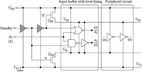
FIGURE 7.29
Switched-source-impedance scheme applied to memory LSI to make internal nodes of RAMs predictable. Enhanced-Vth transistors are used for QSP and QSN and the shaded inverters. (“Switched-Source-Impedance CMOS Circuit For Low Standby Sub-threshold Current Giga-Scale LSI’S”, M. Horiguchi et al., IEEE J. Solid-State Circuits, Vol. 28, pp. 1131–1135, 1993.)
7.13 Analysis of Sub-Threshold Leakage Reduction
Different techniques for reducing sub-threshold leakage in CMOS digital circuits have been proposed and are briefly discussed in previous sections. These techniques have broadly been classified as (1) leakage control in standby mode, and (2) leakage control in active mode. Fairly good analysis of all these techniques has been made in ref. [92] while using a 28-transistor standard 1-bit full adder with the TSMC 180 nm technology circuit. The analysis is based on the following performance criteria: leakage power dissipation, dynamic power dissipation, and propagation delay.
One of the options for reducing leakage is to cut off supply from the circuit during sleep mode. Important techniques in this category are (1) power gating, and (2) super cutoff CMOS (SCCMOS). Power gating is done using either NMOS or PMOS only or both NMOS and PMOS having high Vth. With only PMOS gating, 9× reduction was achieved in leakage power, but delay was 1.046× and there was a slight increase in dynamic power. For only NMOS gating leakage power was reduced up to 12× with delay increase of 1.084× and again a small increase in dynamic power consumption. With both NMOS and PMOS gating leakage power was reduced by two orders of magnitude but with increase in delay of 1.14×. In the SCCMOS reduction in leakage power comparative to two sleep transistor circuits is less; at the same time, the delay introduced also becomes less. The technique has further advantage of easier fabrication, as all transistors are realized with standard Vth.
Important techniques for reducing leakage in active mode analyzed using 1 bit full adder were forced stacking, input vector control (IVC), and sleepy stack. In the forced stacking technique leakage saving was up to 1.45× but delay was increased by 1.025×. The IVC technique provides higher saving in leakage power but an exhaustive simulation is required for determining critical input vector. Use of sleepy stack gave lesser reduction in leakage power, but propagation delay improves, and it also requires a little complicated signal circuitry. The analysis confirms a strong correlation among the three important factors of leakage power, dynamic power, and propagation delay.
Different leakage reduction techniques for the active mode of operation like reverse body biasing (RBB), forced stacking, input vector control (IVC), and use of high Vth MOSFET have been analyzed from the point of view of finding the effect of technology scaling. For the purpose of analysis, inverter, two and three input NAND and NOR gates were simulated using predictive technology models at 65 nm, 45 nm and 32 nm and its important observations are as follows [93]. Use of high Vth MOSFETs scales well with technology in both active as well as standby modes of operation and reduces the leakage with only small performance degradation. The RBB scheme has been found to be less effective with technology downscaling because of increased band-to-band tunneling (BTBT) current and the scaling of body effect coefficient. After an optimum RBB value, its value decreases with scaling [94]. With technology scaling, pin ordering was found to be attractive at low voltage levels as it could be combined with any other technique for leakage reduction, with minimal adverse impact. Another point of consideration is the comparative bigger size of PMOSs in pull up blocks, thus having bigger leakage component. Hence transistor sizing assumes significance. In addition, logic manipulation can also result in an implementation with low leakage logic gates.
7.14 Sub-Threshold Leakage Reduction for Low-Voltage Applications
It was expected that supply voltage would be scaled down to below 0.5 V and the leakage power would become a dominant component even in the active mode of operation, unless the threshold voltage is more than 0.1 V [95]. In a slightly different technique, dynamic threshold voltage hopping (Vth-hopping) is used in which dynamic adjustment of clock frequency and Vth is done through back-gate bias variation based on the workload of the system. Figure 7.30 shows the schematic of the Vth-hopping method. Here the power control block generates signals as shown which in turn controls substrate bias of the system. Control signal is controlled by software through a software feedback loop scheme [70]. The clock frequency has only the values of fCLK, fCLK/2, and so on, to avoid any synchronization problem at the interface. Frequency controller generates fCLK and fCLK/2, with Vth low-enable and Vth high-enable assertion, respectively. Determination of Vthlow and Vthhigh is based on the maximum achievable performance of the processor at the clock frequency fCLK and fCLK/2, respectively. An important consideration in the scheme is that the back-gate bias is possible for its positive and negative values for the Vth-hopping. Such a combination is suitable for reduced technology node. Value of Vthlow and Vthhigh is to be determined for maximum performance in such a way that system works at the possible discrete frequencies as mentioned above. Hence, an algorithm to dynamically change the Vth depending on the variation of the workload is important. The applied algorithm is based on the run-time voltage hopping scheme [96]. It was observed that the Vth-hopping scheme can achieve up to 82% power reduction compared to the fixed low-Vth circuits when 0.5 V power supply is used. A similar range of power saving was obtained in a RISC processor where zero back-gate bias was applied in comparison to a fixed positive back-bias.
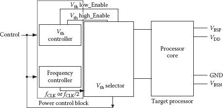
FIGURE 7.30
Schematic diagram of VTH-hopping. (Redrawn from “VTH-Hopping Scheme to Reduce Sub-threshold Leakage for Low-Power Processors”, K. Noise et al., IEEE J. Solid-State, Vol. 37, pp. 413–419, 2002.)
SRAMs have been very successful in embedded memories. However, at low voltage level of 0.5 V VDD, DRAMs are favorable to replace SRAMs mainly because of the non-scalability of its Vth which stays at about 1 V [97]. DRAMs are more immune to the Vth variation at VDD of 0.5 V, and active power consumption is heavily reduced, making it a preferred memory for mobile applications. A low voltage DRAM at 0.5 V VDD needs suitable sense amplifier (SA) and word line boosters. High performance, SAs are available and discussed in Chapter 8 [98,99]. A number of circuits for another key element-word line booster are available, however conventional boosters suffered from either Vth loss or inefficient charge transfer mechanism. An efficient booster overcoming the problem of Vth loss is given by Tanakamaru and Takeuchi, which generates word-line voltage VPP of 1.4 V for 0.5 V DRAM operations [100]. This booster raises VPP from 0.5 V to 1.4 V within three clock cycles compared to other boosters which take eight clock cycles to raise VPP to 1.4 V. Another major advantage of the booster is its reduced power consumption of 60 pJ which is ~68% of the conventional circuits.
7.15 Data Retention Time and Its Improvement
In Section 7.8, it was shown that as the DRAM size M increases, say quadrupled, then both, the number of cells in a word line m and the maximum refresh time tREF max are doubled. Increase in m and tREF max is necessary to keep power consumption due to cell leakage in control and maintain constant refresh interval independent of DRAM density increase. Because of this continued rise in the value of tREF max, study of retention time, defined as the time duration during which stored cell signal can be read reliably, became extremely important. The retention time has to be increased with every successive generation; otherwise, reliability and functionality of the DRAM shall be at stake.
For the purpose of enhancing retention time, its distribution was plotted as a function of boron concentration of a p-well for a specific memory cell; studies revealed a very significant aspect. It was observed that the distribution of the retention time is clearly divided in two parts: (1) a main distribution, having longer retention time and almost all the cells in memory came under this category, and (2) a tail distribution, which corresponds to a few memory cells with a shorter retention time [5]. For example with an average retention time of 6 s at 85°C retention time of normally distributed probability, retention time of the worst case is 100 ms at 5 sigma spread. This problematic tail distribution depends proportionally on the boron concentration of the p-well. Hence, it was obvious that for the overall increase in the retention time, it is very important to reduce the tail distribution. Suggested methods include (1) reduction in the boron concentration of p-well which will reduce electric field of the depletion layer at storage node-p-n junctions, and (2) reduction of concentration of the deep level of thermionic field emission (TFE) current; TFE is a concept introduced for understanding of a relationship of tail distribution with boron concentration [6]. It is known that deep level TFE is related with interstitial silicon; hence, tail distribution can be improved by controlling the generation of point defects. Unless measures were taken to reduce the small number of problematic cells with shorter retention time, practical fabrication would become impossible.
Other studies have also been made for finding an explanation of leakage during tail modeling of the memory cell junction as a two-terminal p-n junction [101,102] as well as a three-terminal structure [103] taking into consideration the effect of gate electrode as well. It is concluded that GIDL also contributes to the leakage in weak cells in the tail. It is important, therefore, that GIDL current has to be controlled and reduced for improving data retention. It is confirmed in another study on an 80 nm RCAT technology [104] that GIDL current is a major component in determining the value of retention time. First, total leakage current is modeled as a combination of storage node leakage current and GIDL current. Using trap-assisted-tunneling model for the two current, maximum electric fields are evaluated as a function of bias conditions. The leakage model is then filled to reproduce tRET (data retention time) for different bias values of VDS, VGS, and VBS, and the results confirm the contribution of GIDL as mentioned before.
Using retracted Si3N4 liner STI, a novel cell transistor is realized for improving the data retention time of high-density DRAMs in 0.15 μm technology. Use of retracted Si3N4 liner STI and optimized channel doping profile, from the point of view of local area electric field in the depletion region, reduces maximum electric field from channel to drain by about 15%. With reduction in maximum electric field, the junction leakage current of weak cells decreases and tail component of data retention improves [105].
Application of innovation in the fabrication process for improving DRAM retention time has further been used for sub-60 nm technology overcoming some limitations of existing devices. Recessed channel transistor, RCAT and SRCAT, discussed in Sections 4.2 and 4.2.1, respectively, have been employed extensively below 80 nm technologies to overcome the limitation of short-channel effect. However, they have higher body effect and sub-threshold slope in comparison to planar transistor and the effects are compounded due to the shrinking of feature size because of edge effect [106] of shallow trench isolation (STI). A new active isolation structure Lat Ex (lateral extended) has been adopted in an SRCAT to improve the data retention time. Figure 7.31 shows the schematic of the Lat Ex actively deployed in recessed channel structure, and it is compared with a conventional structure in terms of active area and S/D regions [107]. Junction leakage and GIDL current, both responsible for tail distribution of leakage current, are considerably reduced. One of the reasons for this is that band-to-band tunneling is reduced, affecting GIDL. Sub-threshold slope could be lowered up to 30% and the body effect is improved from 400 mV/V to 350 mV/V. As a result of these improvements in the characteristics of SRCAT, data retention characteristics become much better than a conventional SRCAT. It was expected that Lat Ex will be suitable even beyond 60 nm technology. Another attempt has been made employing RCAT and applying negatively biased off-state of the word line (NWL) to improve the sub-threshold characteristics of the cell transistor [108]. It was observed that the cumulative fail bit count (FBC) of the retention time main distribution decreases as NWL bias is strengthened. However, it was not so effective for the tail distribution because of its lesser effect on GIDL current. Therefore, a suitable NWL bias scheme and a magnitude of cell transistor threshold voltage are needed for full acceptability of the scheme.
FIGURE 7.31
Schematic showing reduction in the area of channel depletion layer region and the area of S/D region in the Lat Ex active compared to conventional device at left. (“Lateral-Extended (Lat Ex.) Active for Improvement of Data Retention Time for Sub 60 nm DRAM Era”, S. Lee et al., Sol. State-Device Research (ESSDRC), pp. 327–329, 2007.)
It was suggested earlier that data retention time can also be improved by reducing vacancy-type defects in DRAM cell transistors because the amount of junction leakage current depends on it as well. The idea was pursued in a report indicating that the enhanced junction leakage current is due to triangular intrinsic stacking faults in the depletion layer of minority bits, through a trap-assisted tunneling [109]. Effort was made to control the defect growth through lattice strain, but success was insufficient and it was concluded that a small number of vacancy-type defects, like point, still remain [110]. Further study showed that reduction of silicon interstitials caused vacancy-type defect generation during annealing. Hence, a reverse annealing was used to reduce such defects, which helps supply a large number of silicon atoms as illustrated in Figure 7.32. Data retention time of both majority and minority bits in a 0.11 μm technology DRAM was improved considerably. This report also gives a useful relationship between number of tail bits and the vacancy-type defect density [110]. Silicon atoms are absorbed in polysilicon during high-temperature annealing and remaining vacancies can generate vacancy-type defects, whereas in reverse annealing condition, interstitials are generated in the silicon substrate.
FIGURE 7.32
(a) Schematic diagram showing a possible reason for vacancy-type defects. (b) Under the reverse annealing condition, a large number of silicon interstitials are generated in the silicon substrate. (Redrawn from “Improvement of Data Retention Time Property by Reducing Vacancy-Type Defects in DRAM Cell Transistors”, K. Okonogi et al., IEEE 44th Annual Int. Relia. Physics Symp., pp. 695–696, 2006.)
It is well established that tail component cells have an order of magnitude higher cell junction leakage current and GIDL current. The latter becomes especially serious in recessed-channel array transistors which are more likely to be used in sub-80 nm technology level. It is also known that the GIDL is primarily determined by the distribution of traps within a cell storage junction [111] and the current is generated by trap-assisted tunneling (TAT). These problematic cells with large leakage current are only a few parts per million and are generated during different fabrication processes such as high-power plasma etching, oxidation, annealing, and so on. Recent study has shown that the electric field at the gate overlapped source/drain region and the spatial location or energy levels of traps are the most important factors contributing toward higher leakage [112]. Only a small number of deep level traps primarily contribute the tail distribution and GIDL current dispersion due to TAT. If the deep traps are somehow excluded from high electric field region, and the number of traps is reduced, then the tail distribution cannot only be minimized, it can be eliminated, thereby increasing the data retention time corresponding to that of only main distribution.
For better understanding, three specimens of 1 Gbit DRAM at 100 nm, 60 nm, and 50 nm technology nodes were studied. The trap density per unit cell (Dit*) at Si/SiO2 interface is estimated, which is then digitized. It gives an important result in that most cells realized in about 10 nm scale do not contain any traps; only a few have them. This means that the storage cells have defects or not; therefore, tail distribution shall not be present in the majority of the cells, which will have data retention times of several tens of seconds provided care is taken during the fabrication processes to minimize/eliminate reasons for the production of deep level traps especially in stronger electric field areas.
It is observed in a recent report that if passivation annealing is performed prior to the deposition of plasma nitride layer in DRAMs, it can improve junction leakage current considerably. It happens as crystalline defects are repaired due to sufficient generation of hydrogen when such a passivation annealing process is used [113]. In addition, variation in transistor threshold Vth is also reduced which enables a reduction in electric field and consequential reduction in leakage current. As a result DRAM data retention is improved further.
1. M. Aoki et al., “A 1.5V DRAM for Battery-Based Applications,” IEEE I.S.S.C. Conference, pp. 238–239, 349, 1989.
2. Y. Nakagome et al., “A 1.5V Circuit Technology for 64 MB DRAMs,” Symp. VLSI Circuits, pp. 17–18, 1990.
3. J.Y. Kim et al., “The Excellent Scalability of the RCAT (Recess Channel-Array-Transistor) Technology for Sub-70 nm DRAM Feature Size and Beyond,” Int. Symp. VLSI Techn., pp. 33–34, 2005.
4. K. Itoh, K. Sasaki, and Y. Nakagome, “Trends in Low-Power RAM Circuit Technologies,” Proc. IEEE, Vol. 83, no. 4, pp. 524–543, 1995.
5. T. Hamamoto, S. Sugiura, and S. Swada, “On the Retention Time Distribution of Dynamic Random Access Memory (DRAM),” IEEE Trans. Electr. Dev., Vol. 45, no. 6, pp. 1300–1309, 1998.
6. S.M. Ze, Physics of Semiconductor Devices, New York, Wiley, 1981, pp. 84–96.
7. D.J. Frank, “Power-Constrained CMOS Scaling Limits,” IBM J. Res. and Dev., Vol. 46, pp. 235–244, 2002.
8. Y. Nakagome et al., “Review and Future Prospects of Low-Voltage RAM Circuits,” IBM J. Res. and Dev., Vol. 47, no. 5/6, pp. 525–552, 2003.
9. T. Inukai and T. Hiramoto, “Suppression of Stand-By Tunnel Current in Ultrathin Gate Oxide MOSFETs by Dual Oxide Thickness MTCMOS,” Int. Conf. S.S. Dev. and Mat., pp. 264–265, 1999.
10. K. Kimura et al., “Power Reduction Techniques in Megabit DRAMs,” IEEE J. Solid State Circ., Vol. SC-21, pp. 381–389, 1986.
11. Y. Watanabe et al., “Offset Compensating Bitline Sensing Scheme for High Density DRAMs,” J. Solid State Circuits, Vol. 28, pp. 9–13, 1994.
12. S.H. Hong et al., “An Offset Cancellation Bit-Line Sensing Scheme for Low-Voltage DRAM Applications,” ISSCC Dig. Tech. Papers, pp. 154–155, 2002.
13. T. Nagai et al., “A 17 ns 4-Mb CMOS DRAM,” J. Solid State Circuits, Vol. 25, pp. 1538–1543, 1991.
14. J.Y. Sim et al., “A 1.0V 256 Mb SDRAM with Offset-Compensated Direct Sensing and Charge-Recycled Precharge Scheme,” ISSCC Dig. of Tech. Papers, pp. 310–311, 2003.
15. S.S. Eaton et al., “A 100 ns 64 K Dynamic RAM Using Redundancy Techniques,” ISSCC, pp. 84–85, 1981.
16. K. Itoh, “Trends in Megabit DRAM Circuit Design,” IEEE J. Solid State Circuits, Vol. 25, no. 3, pp. 778–788, 1990.
17. K. Itoh et al., “An Experimental 1 Mb DRAM with On-Chip Voltage Limiter,” ISSCC, pp. 282–283, 1984.
18. T. Sugibayashi et al., “A 30 ns 256 Mb DRAM with Multidivided Array Structure,” ISSCC Dig. Tech. Papers, pp. 50–51, 1993.
19. K. Fujishima et al., “A 256K Dynamic RAM with Page-Nibble Mode,” IEEE J. Solid State Circuits, Vol. SC-18, pp. 470–478, 1983.
20. T. Yoshihara et al., “A Twisted Bit Line Technique for Multi-Mb DRAMs,” ISSCC, pp. 238–239, 1988.
21. H. Hidaka et al., “Twisted Bit-Line Architecture for Multi-Megabit DRAMs,” IEEE J. Solid State Circuits, Vol. 24, pp. 21–27, 1989.
22. M. Aoki et al., “An Experimental 16-Mbit DRAM with Transposed Data-Line Structure,” ISSCC Dig. Tech. Papers, pp. 250–251, 1988.
23. J.K. DeBrose, J.E. Lary, and E.-J. Sprogis, “Signal Twist Layout and Method for Paired Line Conductors of Integrated Circuits,” 1996 U.S. Patent, 5,534, 732.
24. M. Aoki et al., “A 1.5V DRAM for Battery-Based Applications,” Proc. Int. SS. Cir. Conf., pp. 238–239, 1989; and also IEEE J.S.S.Cir., Vol. 24, pp. 1206–1212, 1989.
25. K. Kim, C. Hwang, and J. Lee, “DRAM Technology Perspective for Gigabit Era,” IEEE Trans. Elect. Dev., Vol. 45, pp. 598–608, 1998.
26. D.-S. Min and D.W. Langer, “Multiple Twisted Data Line Technique for Coupling Noise Reduction in Embedded DRAMs,” IEEE Custom Int. Cir, Conf., pp. 231–234, 1999.
27. D.-S. Min and D.W. Langer, “Multiple Twisted Data Line Techniques for Multigigabit DRAMs,” IEEE J. Solid State Circ., Vol. 34, pp. 856–865, 1999.
28. T. Yamagata et al., “Low Voltage Circuit Design for Battery-Operated and/or Giga DRAMs,” IEEE J. Solid State Circuits, Vol. 30, pp. 1183–1188, 1995.
29. T. Mano et al., “Submicron VLSI Memory Circuits,” IEEE, ISSCC, pp. 234–235, 311, 1983.
30. H. Tanaka et al., “Stabilization of Voltage Limiter Circuit for High-Density DRAM’s Using Pole-Zero Compensation,” IEICE Trans. Electron., Vol. E 75-C, no. 11, pp. 1333–1343, 1992.
31. D. Chin et al., “An Experimental 16-Mbit DRAM with Reduced Peak Current Noise,” IEEE J. Solid State Circ., Vol. 24, pp. 1191–1197, 1989.
32. M. Horiguchi, “A Tunable CMOS-DRAM Voltage Limiter with Stabilized Feedback Amplifier,” IEEE J. Solid State Circ., Vol. 25, no. 5, pp. 1129–1135, 1990.
33. M. Horiguchi et al., “Dual-Operating-Voltage Scheme for a Single 5V 16 Mbit DRAM,” IEEE J. Solid State Circ., Vol. 23, pp. 612–617, 1988.
34. T. Furuyama et al., “A New On-Chip Voltage Converter for Sub-micrometer High-Density DRAM’s,” IEEE J. Solid State Circ., Vol. SC-22, pp. 437–441, 1987.
35. M. Takada et al., “A 4 Mb DRAM with Half Internal Voltage Bit Line Precharge,” IEEE J. Solid State Circ., Vol. SC-21, pp. 612–617, 1986.
36. G. Kitsukawa et al., “A 1 Mbit Bic MOS DRAM Using Temperature-Compensated Circuit Techniques,” IEEE J. Solid State Circ., Vol. 24, pp. 597–602, 1989.
37. M. Akasura et al., “A 34 ns 256 Mb DRAM with Boosted Sense-Ground Scheme,” Proc. SSCC, pp. 140–141, 1994.
38. D. Takashima et al., “Low Power On-Chip Supply Voltage Conversion Scheme for 1G/4G bit DRAMs,” Symp. on VLSI Circuits Digest of Tech. Papers, pp. 114–115, 1992.
39. H. Tanaka et al., “A Precise On-Chip Voltage Generator for a Giga-Scale DRAM with a Negative Word-Line Scheme,” Symp. VLSI Circ. Dig. Tech. Papers, pp. 94–95, 1998.
40. Y. Tsukikawa et al., “An Efficient Back-Bias Generator with Hybrid Pumping Circuit for 1.5V DRAMs,” Symp. VLSI Circ. Dig. Tech. Papers, pp. 85–86, 1993.
41. M. Horiguchi et al., “Dual-Regulator Dual-Decoding-Trimmer DRAM Voltage Limiter for Burn-in Test,” IEEE J. Solid State Circ., Vol. 26, no. 11, pp. 1544–1549, 1991.
42. H. Tanaka et al., “Sub-1-μA Dynamic Reference Voltage Generator for Battery-Operated DRAM,” Symp. VLSI Circ. Dig. Tech. Papers, pp. 87–88, 1993.
43. K. Sato et al., “A 4-Mb Pseudo SRAM Operating at 2.6 ± 1V with 3-μ,A Data Retention Current,” IEEE J. Solid State Circ., Vol. 26, pp. 1556–1562, 1991.
44. Y. Kagenishi et al., “Low Power Self Refresh Mode DRAM with Temperature Detecting Circuits,” VLSI Circ. Symp., pp. 43–44, 1993.
45. D.-C. Choi et al., “Battery Operated 16 M DRAM with Post Package Programmable and Variable Self Refresh,” Symp. VLSI Circ. Dig. Tech. Papers, pp. 83–84, 1994.
46. J. Nyathi and J. Delgado-Frias, “Self-Times Refreshing Approach for Dynamic Memories,” Proc. Annual Int. ASIC Conf., pp. 169–173, 1998.
47. Influent Corp., “Reducing Server Power Consumption by 20% with Pulsed Air Cooling,” June 2009, http://www.influentmotion.com/ServerWhitepaper.pdf.
48. L. Minas and B. Ellison, “The Problem of Power Consumption in Server,” Intel Press Report, 2009.
49. Micron, “TN-47-16 Designing for High Density DDR2 Memory Introduction,” 2005.
50. JEDEC Committee JC-42-3, “JESD79-3D,” Sept. 2009.
51. Y. Idei et al., “Dual-Period Self-Refresh Scheme for Low Power DRAMs with On-Chip PROM Mode Register,” IEEE J. Solid State Circ., Vol. 33, pp. 253–259, 1998.
52. S. Takase and N. Kushiyama, “A 1.6 Gb/s DRAM with Flexible Mapping Redundancy Technique and Additional Refresh Scheme,” Proc. Int. Sol. State Circ. Conf., pp. 410–411, 1999.
53. J. Kim and M. Papaefthymiou, “Dynamic Memory Design for Low Data-Retention Power,” Proc. PATMOS, 10th Int. Workshop, pp. 207–216, 2000.
54. J. Kim and M. Papaefthymiou, “Block-Based Multiperiod Dynamic Memory Design for Low Data-Retention Period,” IEEE Trans. on VLSI Systems, Vol. 11, pp. 1006–1018, 2003.
55. J. Stuecheli et al., “Elastic Refresh: Techniques to Mitigate Refresh Penalties in High Density Memory,” 43rd IEEE/ACM Int. Symp. on Microarchitecture, pp. 375–384, 2010.
56. M.J. Lee and K.W. Park, “A Mechanism for Dependence of Refresh Time on Data Pattern in DRAM,” IEEE Elect. Dev. Lett., Vol. 31, pp. 168–170, 2010.
57. S. Mutoh et al., “1-V Power Supply High-Speed Digital Circuit Technology with Multithreshold-Voltage CMOS,” IEEE J. Solid State Circuits, Vol. 30, pp. 847–854, 1995.
58. S. Shigematsu et al., “A 1-V High-Speed MTCMOS Circuit Scheme for Power-Down Applications,” Symp. VLSI Circuit, Dig. Tech. Papers, pp. 125–126, 1995.
59. H. Akamatsu et al., “A Low Power Data Holding Circuit with an Intermittent Power Supply Scheme for Sub-1V MT-CMOS LSIs,” Symp. VLSI Circuits, Dig. Tech. Papers, pp. 14–15, 1996.
60. Z. Chen et al., “0.18 μm Dual Vt MOSFET Process and Energy-Delay Measurement,” Proc. IEDM, pp. 851–854, 1996.
61. S. Heo and K. Asanovic. “Leakage-Based Domino Circuits for Dynamic Fine-Grain Leakage Reduction,” Symp. VLSI Circuits, Dig. Tech., Papers, pp. 316–319, 2002.
62. S. Thompson et al., “Dual Threshold Voltages and Substrate Bias: Keys to High Performance, Low Power, 0.1 μm Logic Design,” Symp. VLSI Tech. Dig. Tech. Papers, pp. 69–70, 1997.
63. H. Oyamatsu et al., “Design Methodology of Deep Submicron CMOS Devices for 1V Operation,” IEICE Trans. Electron., Vol. E79-C, pp. 1720–1724, 1996.
64. L. Wei et al., “Design and Optimization of Dual-Threshold Circuits for Low-Voltage Low-Power Applications,” IEEE Trans. VLSI Systems, Vol. 7, pp. 16–24, 1999.
65. Zhamping Chen et al., “Estimation of Standby Leakage Power in CMOS Circuits Considering Accurate Modeling of Transistor Stacks,” ISPLED, pp. 239–244, 1998.
66. S. Nareandra et al., “Scaling of Stack Effect and Its Application for Leakage Reduction,” ISPLED, pp. 195–200, 2001.
67. K. Das and R. Brown, “Novel Ultra Low-Leakage Power Circuit Techniques and Design Algorithm in PD-SOI for Sub-1V Applications,” Proc. Internation. SOI Confer., pp. 88–90, 2002.
68. K. Das et al., “New Optimal Design Strategies and Analysis of Ultra-Low Leakage Circuits for Nano-Scale Technology,” Proc. ISLPED, pp. 168–171, 2003.
69. International Technology Roadmap for Semiconductors, http://public.itrs.net/Files/2001.ITRS/Home.hlm, 2001 Edition.
70. R.M. Rao, J.F. Burns, and R.B. Brown, “Analysis and Optimization of Enhanced MTCMOS Scheme,” Proc. 17th International Conf. VLSI Design (VLSID’04), 2004.
71. J.C. Park and V.J. Mooney, “Sleepy Stack Leakage Reduction,” IEEE Trans. VLSI Systems, Vol. 14, pp. 1250–1263, 2006.
72. J.T. Kao and A.P. Chandrakasan, “Dual-Threshold Voltage Techniques for Low-Power Digital Circuits,” IEEE J. Solid State Cir., Vol. 35, pp. 1009–1018, July 2000.
73. J. Kao, S. Narendra, and A. Chandrakasan, “MTCMOS Hierarchical Sizing Based on Mutual Exclusive Discharge Pattern,” ACM/IIEEE Design Automation Conf., pp. 495–500, June 1998.
74. T. Sakuta, W. Lee, and P. Balsara, “Delay Balanced Multipliers for Low Power/Low Voltage DSP Core,” IEEE Symp. Low Power Electronics, pp. 36–37, 1995.
75. J. Kao, “Dual Threshold Voltage Domino Logic,” 25th Eur. Solid State Circuit Conf., pp. 118–121, Sept. 1999.
76. G. Kitsukawa et al., “256 Mb DRAM Technologies for the File Applications,” IEEE J. Solid State Circ., Vol. 28, pp. 1105–1111, 1993.
77. T. Kawahara et al., “Subthreshold Current Reduction for Decoded-Driver by Self-Reverse Biasing,” IEEE J. Solid State Circuits, Vol. 28, pp. 1136–1143, 1993.
78. Y. Nakagome et al., “Sub-1-V Swing Bus Architecture for Future Low Power VLSIs,” Symp. VLSI Circuits, Dig. Tech. Papers, pp. 82–83, 1992.
79. H. Kawaguchi, K. Nose, and T. Sakurai, “A Super Cut-Off CMOS (SCCMOS) Scheme for 0.5V Supply Voltage with Pico Ampere Stand-by Current,” IEEE J. Solid State Circuits, Vol. 35, pp. 1498–1501, 2000.
80. K. Seta et al., “50% Active-Power Saving without Speed Degradation Using Standby Power Reduction (SPR) Circuits,” ISSCC, pp. 318–319, 1995.
81. T. Kuroda et al., “A 0.9V, 150 MHz, 10 mW, 4 mm2, 2-D Discrete Cosine Transform Core Processor with Variable-Threshold-Voltage Scheme,” ISSCC Dig. Tech. Papers, pp. 166–167, 1996.
82. H. Mizuno et al., “A 18-μA Standby Current 1.8V 200 MHz Microprocessor with Self-Substrate-Based Data Retention Mode,” IEEE J. Solid-State Cir., Vol. 34, pp. 1492–1500, 1999.
83. S.V. Kosonocky et al., “Enhanced Multi-Threshold (MTCMOS) Circuits Using Variable Well Bias,” Proc. ISPLED, pp. 165–169, 2001.
84. M. Mizuno et al., “Elastic-VT CMOS Circuit for Multiple On-Chip Power Control,” ISSCC, pp. 300–301, 462, 1996.
85. K. Kumagi et al., “A Novel Powering-down Scheme for Low Vt CMOS Circuits,” Symp. VLSI Circuits, Dig. Tech. Papers, pp. 44–45, 1998.
86. M.J. Lee and K.W. Park, “A Mechanism for Dependence of Refresh Time on Data Pattern in DRAM,” IEEE Elect. Dev. Lett., Vol. 31 (2), pp. 168–170, 2010.
87. M.J. Lee, K.W. Park, and J.H. Ahn, “Selective Negative Word Line Scheme for Improving Refresh,” Electronic Letters, Vol. 47, No. 3, Feb., 2011.
88. K. Sato, et al., “A 20 ns Static Column 1 Mb DRAM in CMOS Technology,” IEEE, ISSCC Dig. Tech. Papers, pp. 254–255, 1985.
89. D.S. Lee, Y.H. Jun, and B.S. Kong, “Simultaneous Reverse Body and Negative Word-Line Biasing Control for Leakage Reduction of DRAM,” IEEE J. Solid State Circ., Vol. 46, pp. 2396–2405, 2011.
90. M. Horiguchi et al., “Switched-Source-Impedance CMOS Circuit for Low Standby Subthreshold Current Giga-Scale LSI’S,” IEEE J. Solid State Circuits, Vol. 28, pp. 1131–1135, 1993.
91. J.P. Halter and F.N. Najm, “A Gate-Level Leakage Power Reduction Method for Ultra-Low Power CMOS Circuits,” IEEE Custom. Integ. Cir. Conference, pp. 475–478, 1997.
92. B.S. Deepaksubramaniam and A. Nunez, “Analysis of Subthreshold Leakage Reduction in CMOS Digital Circuits,” 50th Midwest Symp. Circuits and Systems (MWSCAS), pp. 1400–1404, 2007.
93. P. Ghafari, M. Anis, and M. Elmesry, “Impact of Technology Scaling on Leakage Reduction Techniques,” North East Workshop on Circuits and Systems, NEWCAS, pp. 1405–1408, 2007.
94. A. Keshavarzi et al. “Technology Scaling Behavior of Optimum Reverse Body Bias for Standby Leakage Power Reduction in CMOS IC’s,” ISLPED, pp. 252–255, 1999.
95. K. Nose et al., “VTH-Hopping Scheme to Reduce Subthreshold Leakage for Low-Power Processors,” IEEE J. Solid State Circuits, Vol. 37, pp. 413–419, 2002.
96. S. Lee and T. Sakurai, “Run-Time Voltage Hopping for Low-Power Real-Time Systems,” IEEE/ACM Proc. Design Automation Conf., pp. 806–809, 2000.
97. K. Itoh, M. Horiguchi and M. Yamaoka, “Low-Voltage Limitations of Memory-Rich Nano Scale CMOS LSIs,” Proc. Eur. Solid State Circuits Conf., pp. 68–75, 2007.
98. S. Akiyama, et al., “Low-Vt Small-Offset Gated Preamplifier for Sub-1 V Gigabit DRAM Arrays,” IEEE Int. Solid State Cir. Conf., Dig. Tech. Papers, pp. 142–143, 2009.
99. A. Kotabe, et al., “A 0.5 V Low-VT CMOS Preamplifier for Low-Power and High-Speed Gigabit-DRAM Arrays,” IEEE J. Solid-State Cir., Vol. 45, pp. 2348–2355, 2010.
100. S. Tanakamaru and K. Takeuchi, “A 0.5 V Operation VTH Loss Compensated DRAM Word-Line Booster Circuit for Ultra-Low Power VLSI Systems,” IEEE J. Solid-State Cir., Vol. 46, pp. 2406–2415, 2011.
101. A. Hairawa et al., “Local-Field-Enhancement Model of DRAM Retention Failure,” IEDM Tech. Dig., pp. 157–160, 1998.
102. S. Ueno, Y. Irone, and M. Inuushi, “Impact of Two Trap-Related Leakage Mechanisms on the Tail Distribution of DRAM Retention Characteristics,” IEDM Tech. Dig., pp. 37–40, 1999.
103. K. Saino et al., “Impact of Gate-Induced Drain Leakage Current on the Tail Distribution of DRAM Data Retention Time,” IEDM Tech. Dig., pp. 837–840, 2000.
104. W.-S. Lee et al., “Analysis on Data Retention Time of Nano-scale DRAM and Its Prediction by Indirectly Probing the Tail Cell Leakage Current,” IEDM Tech. Dig., pp. 395–398, 2004.
105. J. Lee, D. Ha, and K. Kim, “Novel Cell Transistor Using Retracted Si3N4-Liner STI for the Improvement of Data Retention Time in Gigabit Density DRAM and Beyond,” IEEE. Trans. Electron Devices, Vol. 48, pp. 1152–1157, 2001.
106. H. Fukutome et al., “Direct Measurement of Effects of Shallow-Trench Isolation on Carrier Profiles in Sub-50 nm N-MOSFETs,” Symp. on VLSI Tech., pp. 140–141, 2005.
107. S. Lee et al., “Lateral-Extended (Lat Ex.) Active for Improvement of Data Retention Time for Sub 60 nm DRAM Era,” Sol. State-Device Research (ESSDRC), pp. 327–329, 2007.
108. S. Park et al., “A Novel Method to Analyze and Design a NWL Scheme DRAM,” IEEE, 46th Annual Int. Relia. Physics Symp., pp. 701–702, 2008.
109. K. Okonogi et al., “Lattice Strain Design in W/WN/Poly-Si Gate DRAM for Improving Data Retention Time,” IEDM Tech. Dig., pp. 65–68, 2004.
110. K. Okonogi et al., “Improvement of Data Retention Time Property by Reducing Vacancy-Type Defects in DRAM Cell Transistors,” IEEE 44th Annual Int. Relia. Physics Symp., pp. 695–696, 2006.
111. A. Bouhada, A. Tonhami, and S. Bakkali, “New Model of Gate-Induced Drain Current Density in an NMOS Transistor,” Microelectronic J., Vol. 29, pp. 813–816, 1998.
112. K. Kim and J. Lee, “A New Investigation of Data Retention Time in Truly Nanoscaled DRAMs,” IEEE Electron Dev. Lett., Vol. 30, pp. 846–848, 2009.
113. C.Y. Lee et al., “DRAM Data Retention and Cell Transistor Threshold Voltage Reliability Improved by Passivation Annealing Prior to the Deposition of Plasma Nitride Layer,” IEEE Trans. Dev. Mat. Reliability, pp. 406–412, 2012.