
DRAM organization has been described in Chapter 1. Among the constituents, the core occupies most of the chip area because of the large number of cells replicated in it, whereas peripherals are around it. The shape of the core is either square or rectangular, which makes the dimensions of the row and column decoders and sense amplifiers/drivers well matched with it. It results in proximity between the core and the decoders/sense amplifiers; therefore interconnections occupy less chip space and negligible delay occurs in signal transfer with the core. For the sake of reducing the core (cell) size and improving its performance, some of the performance standards set for a general logic design are compromised. The inherent structured nature of the core is helpful in controlling and minimizing noise generation, which allows relaxing the terms of robustness in comparison to general logic. Another important factor is the reduction in voltage swing at the bit lines during its (dis)charging, though output from the memory is at the full voltage levels. Peripheral circuits now play their role in randomly reaching the cell(s) for reading or writing through row and column buffers and decoders, whereas sense amplifiers help not only in attaining the full voltage level available at the output but also in refreshing the DRAM. The area consumed and the power dissipated by these peripheral circuits also become very important. In addition, propagation delay during access, refreshing, and outputting the signal become extremely important and are considerably affected by the peripherals also. Though the basic structure of row and column decoders has not changed with progressive generations, methods of application have changed with the modes of operation. Sense amplifiers have undergone major changes with the increase in DRAM density and reduction in the availability of sense signal and rise in noise levels due to various reasons. Another important component in the peripherals is the introduction of redundancy and error detection for enhancing the yield. This chapter introduces peripherals and the idea of redundancy.
DRAM operating modes are either asynchronous or synchronous. In synchronous mode all operations are controlled by a system clock, whereas in asynchronous DRAM, control signals and are used for reading, writing, refreshing, and so on. Most of the initial DRAMs were asynchronous; however, to increase data read, frequency synchronous modes were adopted. Irrespective of the operating mode, (1) address multiplexing is almost universal, mainly to reduce pin count and hence cost, and (2) random nature of the access of a cell still remains. In simplest form, all DRAM operations start with the lowering of signal, as in this case the chip does not need chip select () signal, and activates row address buffers, row decoders, word line drivers, and bit-line sense amplifiers and then lowers after a certain duration. One of the word lines gets selected and then some of the data from the selected word line is reached at the falling edge of the signal through column address decoder.
Input to a row decoder is an n-bit address and there are 2n available outputs, of which only one output activates a row that contains the memory cell to be selected. In its simplest form, a 1 out of 2n decoder is a collection of 2n, logic gates each with 1n. Each gate can be realized using an n-input NAND gate and an inverter; alternatively, it can be realized by an n-input NOR gate for each row. However, these simple realizations have many constraints. The layout of the wide (many) inputs gate must fit as per the pitch of the word line. In addition, NOR and NAND gates with three or more inputs suffer from large propagation delay which would add to the overall delay of the memory operation. Power consumption of the decoder is also an important consideration. Hence, the decoders are always realized by splitting the logic in terms of gates with two or three inputs only. The initial part of the logic, which decodes the address, is called a predecoder, and the later part, which provides the final output for the word line, is known as a decoder. Figure 8.1(a,b) show the basic schematic of a decoder and its implementation using six-input static CMOS NAND gates: a wide and slow gate. Figure 8.1(c) shows conversion of wider gate into a version of predecoder–decoder. Reduction in the number of inputs to the gates results in considerable improvements in the propagation delay and power consumption of the decoder. For an eight-input decoder, the expression for WLo can be written as
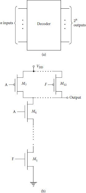
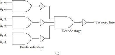
FIGURE 8.1
(a) An n-to-2n binary decoder. (b) Six-input NAND gate. (c) A possible predecoder and decoder configurations with 2 or 3 input gates.
One realization for this case can have two-bit predecoding, which requires both true and false bits. Output predecoders can then be combined in four-input NAND gates for final word line outputs as shown in Figure 8.2. If the predecoder is realized using complementary CMOS logic, number of transistor used in this decoder shall be (256*8) + (4*4*4) + (4*4) = 2128 in place of 4112 (including static inverters) if it was realized in a single stage. Four input NAND decoders can further be converted in more than one logic level containing only two input gates and inverters. An additional advantage of using predecoders is that those decoder blocks which are not selected can be disabled through the addition of a select signal to each predecoder. This results in power saving from the unutilized decoder blocks. Word lines need sufficient capacity decoder drivers for charging and discharging [1], hence proper sizing of the transistors used in the gate becomes important.
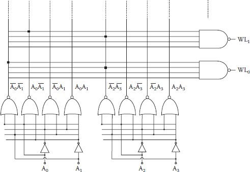
FIGURE 8.2
A NAND decoder using two-input predecoders.
Decoders can also be realized using dynamic logic. Basic forms of dynamic decoders are shown in Figure 8.3(a) and (b); these are 2-to-4 NOR decoder and 2-to-4 NAND decoder, respectively. Point of difference is that the NAND decoder shown is active low type in which selected word line is low, otherwise all lines are normally high. NAND decoders occupy smaller area and consume less power in comparison to NOR decoders but become very slow with increasing size. Hence, for larger decoders, a multilayer approach similar to the static decoder is used.
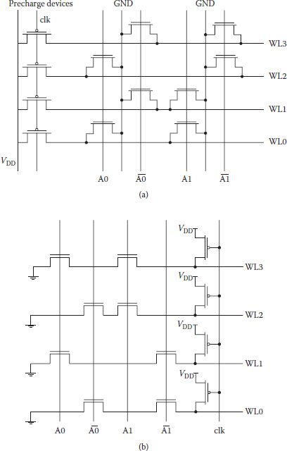
FIGURE 8.3
(a) Dynamic 2-to-4 NOR decoder. (b) A 2-to-4 MOS dynamic NAND decoder. This implementation assumes that all address signals are low during precharge.
Column decoder is essentially a 2M-multiplexer, where M stands for the bits stored in a row (or bits in selected block row for a multi-block DRAM). During the read operation precharged bit lines are to discharge to the sense amplifiers, while during write a low operation bit line has to be driven low. Since read and write operations requirements are slightly different, different multiplexers are often used for the two operations for optimization, though a shared multiplexer is also used.
A simple but costly approach for realizing column decoders is based on pass transistor logic as shown in Figure 8.4(a). Control signals for the pass transistors are generated using a NOR-based predecoder. Advantage of this arrangement is that only one NMOS is on at a time which routes the selected column signal to the data output and makes it very fast. If more than one data is selected, as many transistors can route the output in parallel. However, the main disadvantage of the scheme is the requirement of 2M pass transistors for each bit line and M*2M transistors for the decoder circuit; the scheme becomes prohibitively large for large values of M. In fact, the number of transistors increases further for a shared read-write multiplexer in which instead of NMOS only, a transmission gate-parallel combination of an NMOS and a PMOS is used for the passage of full signal levels.
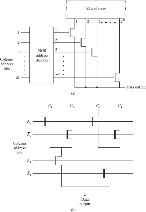
FIGURE 8.4
(a) Bit line (column) decoder arrangement using NOR address decoder and logic pass transistors. (b) Binary tree column decoder circuit for four bit lines.
An alternative scheme using considerably fewer transistors based on binary selection of bits called tree decoder is shown in Figure 8.4(b). As column bit line drives the NMOS pass transistors, NOR decoder is not required, which reduces the total number of transistors considerably. As far as functionality is concerned, pass transistor network selects one out of every two bit lines at each stage. Major drawback of the scheme lies in presence of as many transistors in the data path as the number of address bits, which slows operation for large values of M.
Obviously, choice between the two main schemes depends on a number of factors, like chip area, speed requirement, and memory architecture. Hence, an optimum combination of the two schemes is used where a fraction of bits are predecoded, while the remaining bits are tree decoded.
8.3 Address Decoding Developments
At initial levels of DRAM density, the number of addresses and total number of I/O pins are small. With increased density, time multiplexing was introduced to reduce the pin count (hence the chip cost). Half the address bits were used to select one of the rows, followed by the application of the remaining half address bits to select a particular column. Separate application of row and column bits opened ways to some other methods of reading termed as modes of operation and different methods of address decoding. Some of the developments are briefly discussed in following sections.
8.3.1 Multiplexed Address Buffer and Predecoding
Use of predecoders was shown to result in a drop in the number of transistors required for row and column decoders. As the number of logic level is more than one, predecoding also reduces gate capacitance loading of row/column address drivers. However, for effective address multiplexing, the same address buffer, wherein the address bit information is stored, should be used for the rows and column. To achieve this objective, its address line is disconnected from the column address bus after latching the row address in the row decoder. Additional advantage comes in the form of reduced capacitive loading on the address driver during column access. Figure 8.5(a) shows a basic block form of predecoding with address buffers, where addresses are processed by one of four predecoders. The processing is preceded by storing bit information in an address buffer as shown. A CMOS DRAM address buffer is shown in Figure 8.5(b). A NAND input stage gets activated and samples address information through a CAB clock controlled by / strobes. Bit information is then stored in the latch. A precharge clock presets the address latch to high address state [2]. Additionally, buffers provide drivability and complimentary outputs.
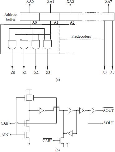
FIGURE 8.5
(a) CMOS dynamic RAM address predecoding scheme. (b) CMOS dynamic RAM address buffer circuit. (Redrawn from “A 70 ns High Density 64 K CMOS Dynamic RAM,” R.J.C. Chwang et al., IEEE J.S.S. Circuits, Vol. SC-18, pp. 457–463, 1983.)
During the 1980s most of the DRAM constituent components were converted from NMOS to CMOS. One of the main reasons was the need in power consumption reduction. In ref. [3] one such attempt was made while using CMOS row decoder in place of NMOS decoder. It was shown that in the CMOS only one decoder was discharging, which meant that capacitance involved was much less than in the NMOS decoder and the power dissipation in the decoder was reduced to only 4% compared to the NMOS version. Another scheme for the suppression of power consumption in CMOS word driver and decoders was given by Kitsukawa et al. [4]. The basic idea in the scheme was the reduction of sub-threshold current up to 3% of the conventional circuits by forcing self-reverse biasing of the driver transistors.
Keeping basic arrangement of buffering, predecoding, and final decoding, changes/improvements have been made in the row decoding with the increasing memory density and changes in the architecture; however, most of these have been associated with SRAM [5,6]. These could well be used with DRAMs and hence a decoder circuit used with a 4.5 Mbit CMOS SRAM is discussed briefly, which is comparatively faster with 1.8 ns access time [7]. For comparison’s sake, a conventional decoder scheme is shown in Figure 8.6(a) and a decoder using source-coupled logic (SCL) circuit, combined with reset circuits, is shown in Figure 8.6(b). In the conventional circuit, transistors turning on during evaluation phase with clock øp are larger than those turning on during precharging. However, it increases precharge delays, and hence large word line-signal pulse width resulting in long cycle time and high power dissipation. A reset signal in Figure 8.6(b) changes transistor aspect ratio which decreases the precharge time in the driver circuit. SCL circuit shown in Figure 8.6(b) provides OR and NOR output simultaneously. Such outputs are suitable for predecoders with large numbers of inputs, hence decoder with SCL circuit operates faster [7]. Combination of reset and SCL circuits reduced address input to word line signal delay by 32%.
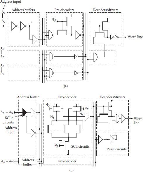
FIGURE 8.6
(a) A Conventional decoder. (b) Decoder using reset circuits and source-coupled-logic (SCL) circuits. (Modified from “A 1.8 ns Access, 550 MHz 4.5 Mb CMOS SRAM,” H. Nimba et al., Proc. ISS. CC. Dig. Tech. Papers, paper SP 22.7, 1998.)
Static column mode operation is similar to the page mode operations but without strobe. Once a row is selected, output from columns is available as per the address as for static RAM. Figure 8.7(a) shows the timing diagram for such an operation [8]. Row addressing is same as that of a multiplex addressed DRAM beginning with the leading edge of strobe. However, for the selection of column, only the address is to be selected and for further reading the next address is to be given without strobe. Obviously, first data output depends on access time like any conventional DRAM. For subsequent read outs, no pre-charging is needed which saves considerable time. Since strobe is not used, operation becomes simpler and faster. Implementation slightly differs in different reports. Figure 8.7(b) shows an arrangement of static column decoder for 1 Mbit DRAM achieving 22 ns column cycle time. The CMOS sense amplifier behaves as static flip-flop once latched, and it is read like a static RAM cell. Sense amplifier is connected to differential I/O bus through NMOS read/write transistors. Static differential comparator feeds the static output buffer once it senses the small signal on the I/O lines. Static write circuit is also used for fast write operation [9].
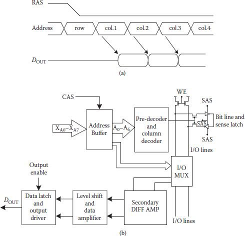
FIGURE 8.7
(a) Timing diagram of a static column DRAM. (Redrawn from “A 64 K DRAM with 35 ns Static Column Operation,” F. Baba et al., IEEE J.S.S. Circuits, Vol. SC-18, pp. 447–451, 1983.) (b) A CMOS dynamic RAM static column design. (Redrawn from “A 1-Mbit CMOS Dynamic RAM with a Divided Bit line Matrix Architecture,” R.T. Taylor and M.G. Johnson, IEEE J.S.S. Circuits, Vol. SC-20, pp. 894–902, 1985.)
An important figure of merit for a 1T1C DRAM cell is the charge transfer ratio given as Cs/(Cs + CBL). Typical value of the charge transfer ratio lies between 0.05 and 0.2, and it becomes a figure of merit of the charge division which occurs when access transistor becomes on. Transfer of charge from storage capacitor makes the readout of the DRAM destructive. In addition, charge of Cs is lost quickly (in a few milliseconds) because of leakages. Therefore, the DRAM must be read continuously (disturbing the stored data) and small changes in the voltage of the bit line detected while reading are converted to the full logic value restored to the cell again. All this is done through the sense amplifier without which 1T1C DRAM cell will not function, in contrast to the SRAM case where the sense amplifier is used to speed up the read process, but it is not essential for the functionality.
8.4.1 Gated Flip-Flop Sense Amplifier
During initial stage of DRAM development, sense amplifiers (SAs) used gated flip-flop as shown in Figure 8.8 [10] which has the advantage of regeneration, and hence small initial unbalance quickly grows to full bias voltage. First, transistor Tc is turned on by clock ϕ3, which connects both nodes of the flip-flop, and it selects dummy word lines on both sides as well. After establishing a precharge voltage on the two nodes, the flip-flop is switched off by switching ϕ2, and ϕ3. For rewriting/refreshing, a storage cell and corresponding dummy word line on the opposite side are selected.
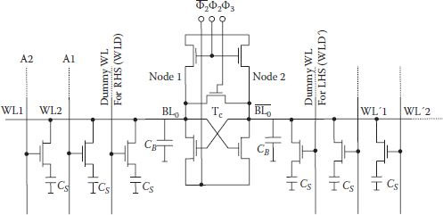
FIGURE 8.8
Sense/refresh circuit with neighboring dummy and storage cells. (“Storage Array and Sense/Refresh Circuit for Single Transistor Memory Cell,” K.U. Stein et al., IEEE J. of Solid State Circuits, Vol. SC-7, pp. 336–340, 1972.)
Depending upon the storage capacitor’s state 1 or 0, small difference in voltage appears across the nodes of the flip-flop. To bring this small voltage to the full value, flip-flop is switched on by ϕ2 and and rewriting/refreshing is done simultaneously in the selected cell and finally the selected word line is deactivated. With basic approach remaining the same, one of the many variants of the basic gated flip-flop is given by Kuo et al. [11]. In this scheme the two bit lines were shorted together as before and a reference voltage level was written into the dummy cell structures. Once a cell is selected, two sides of the flip-flop were disconnected and data from the storage cell was then forced onto one side of the SA opposite to the side where reference level is supplied from the dummy cell onto the flip-flop node. As before, a voltage/charge differential appears across the two nodes of the SA. Load transistors are turned on, and both nodes rise higher, but regenerative action returns full logic back onto the cell very fast. However, a major practical problem with this arrangement still remained. The common mode potential at nodes continued to drift down due to junction leakage of the bit line to substrate. If sufficient time elapsed, charge differential became small enough for proper functioning. To avoid a possible problem from the floating bit line voltage, the circuit was modified by Foss and Harland [12] as shown in Figure 8.9. The two bit lines in this topology are clamped to a reference potential VREF; the rest of the operation is similar to the previous cases. Once voltage/charge differential is set up, the sense clock ϕs grounds the common sources of the flip-flop and regenerative action starts. The load transistors are turned on by ϕL, and the low side rises to a level set by the ratio of the transistor geometries and the high side is pulled to (VDD – Vth).
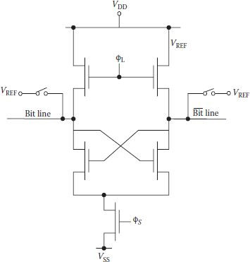
FIGURE 8.9
Sense amplifier given by Ross and Harland. (Redrawn from “Peripheral Circuits for One-Transistor Cell MOS RAM’s,” R.C. Foss and R. Harland, IEEE J. of Solid State Circuits, Vol. SC-10, pp. 225–261, 1975.)
Another variation/modification of the gated flop or cross-coupled latch SA, which retains most of the features of earlier sense amplifiers, is shown in Figure 8.10(a), with three internally generated clocks ϕ0, ϕ1, and ϕ2 and the chip enable . Reference cell is precharged to ground and load transistors are turned on through ϕ2 precharging both bit lines. First, transistor T3 is shut off and simultaneously, T4 and T5 are turned off through ϕ2, so that the reference cell is isolated. Once a row is selected, the reference cell and the selected storage cell are connected to two sides of the SA. Soon T9 is turned on and the signal is amplified on terminals B1 and B2 as shown in Figure 8.10(b). Sensitivity of the SA primarily depends on the threshold balance of the driver transistors T1 and T2, and the accuracy of the reference potential [13].
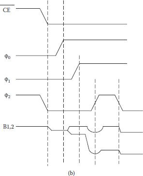
FIGURE 8.10
(a) Schematic of a sense amplifier showing only a single reference and storage cell, and (b) timing signals. (“A 16 384-Bit Dynamic RAM,” C.N. Ahlquist et al., IEEE J. of Solid State Circuits, Vol. SC-11, No. 5, pp. 570–574, 1976.)
8.4.2 Charge-Transfer Sense Amplifier
In the gated flip-flop sense amplifiers, sense signal amplitude (Δν) goes on decreasing with the increase in the bit line capacitance as DRAM density increases, and/or with a decrease in the operating voltage VCC. Along with other noises present, threshold imbalance in the cross-coupled pair of transistor also imposed a limitation on the minimum value of (Δν). Generally, a practical value of CBL/CS ranges between 8 to 10 for correctly reading data in the DRAM. In addition, analysis shows that set time of a latch circuit increases with reduced Δv or increased transistor threshold voltage imbalance [14]. It is therefore essential that for increased density/decreased operating voltage, a sense amplifier should have better sensitivity than the conventional latch. One such method was promoted by Heller and others [15] in which sense signal is not the result of charge redistribution between the bit line capacitance and the storage capacitance, but it is preamplified using a charge-transfer method before feeding the sense signal to the latch. Bit line is then disconnected from the sense amplifier, making the sense signal independent of the bit line capacitance CBL. Figure 8.11 shows the basics of a charge transfer preamplifier circuit and signal variations where charge of the memory cell capacitance CS is transferred to a nearly equal size output capacitor Co through the bit line. However, transistor T2 isolates the highly capacitive bit line and the output capacitance Co, and it can also preamplify the sense signal. Initially the word line is low which keeps Cs and CBL disconnected. When clock ϕ1 is asserted, output voltage rises quickly to high and forces T1 to operate in the ohmic region. Since VR makes T2 always on, bit-line voltage is also raised to (VR – Vth2). Transition of T2 from saturation to cutoff takes place, gate voltage VR is selected such that VR ≤ (VD + Vth2); hence, T2 operates in saturation but moves to cutoff when bit line charges up to (VR – Vth2). Transistor T1 is turned off by lowering ϕ1 and the precharging state completes. Now the word line is raised and for a high stored on Cs bit-line voltage remains unchanged at (VR – Vth2) with T2 still off and output remains a high. However, for CS voltage less than (VR – Vth2), T2 becomes momentarily on as bit line voltage dips by a small amount. Bit line recharges back to (VR – Vth2) as it gets connected to the output and forces T2 again to cut off, while potential of Co drops by ΔV0 = (VR – Vth2 – Vs) Cs/Co. Drop of charge on Co is equal to the gain of charge on Cs and gain of the charge transfer preamplifier is (CBL + Cs)/Co. It is to be noted that the signal level change on Co is independent of the bit line capacitance and threshold voltage of the charge transfer transistor.
The charge transfer circuit output is very well suited for connecting to the flip-flop for further amplification as it needs only two transistors and accepts differential input and write backs and refreshes the cell easily. As shown (within dotted rectangles) in Figure 8.12(a) charge transfer preamplifier circuit blocks, consisting of T1,T2 on the left and T1′, T2′ on the right, are connected to the latch devices T3 and T4. Transistor T6 enables the latch when required and T5 is the bit line equalizer as before. It is important to note that if capacitance at node 1 is higher than Cs, a small sense signal is preamplified into a larger signal.
Read/refresh and write cycle follows the sequence as mentioned below at the time instants cited in Figure 8.12(b). At instant t1 precharging starts as discussed which is essential for read as well as write operation.
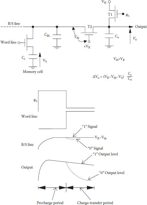
FIGURE 8.11
Charge-transfer preamplifier circuit and signal variations. (“High-Sensitivity Charge-Transfer Sense Amplifier,” L.G. Heller et al., IEEE J. of Solid-State Circuits, Vol. SC-11, pp. 596–601, 1976.)
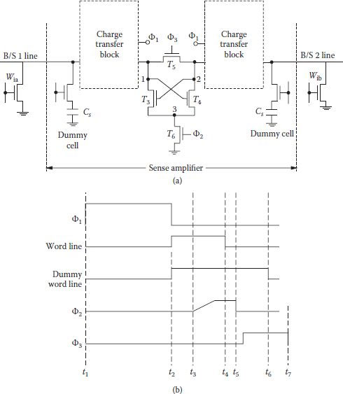
FIGURE 8.12
(a) Balanced charge transfer sense amplifier, and (b) signal variations. (Redrawn from High-Sensitivity Charge-Transfer Sense Amplifier,” L.G. Heller et al., IEEE J. of Solid-State Circuits, Vol. SC-11, pp. 596–601, 1976.)
At instant t2 charge transfer period begins. For a low stored cell, node 1 gains charge, which is lost by the cell, and left-side bit-line voltage is dropped. At the same time the dummy cell on the opposite side of the active cell is accessed, and it transfers half as much charge to node 2, dropping its potential nearly half as much as that at node 1. For the write cycle, instead of raising ϕ2, data is written on bit line and latch proceeds to complete the writing and the word line is made low. By the time instant t3 differential voltage between nodes 1 and 2 is established and T6 is made on slowly, which pulls down node 3 which in turn makes transistor T3 on, but at such a rate that potential at node 1 does not enable transistor T4. Transistor T2 works in linear region and left bit line reaches low level. At t4 word line is made off, so Cs gets disconnected from the left bit line and low remains stored/refreshed.
At instant t5, T6 becomes off and T5 becomes on through ϕ2 and ϕ3, respectively, and potential of the left bit line equalizes to that of the right side bit line to a middle level stored in the dummy cell. At instant t6, the cycle ends; ready for next precharge and at t7 nodes 1 and 2 become isolated.
A further modified and improved charge transfer circuit was given by Heller which increased preamplification speed through cross-coupling of isolation transistors of its earlier version [16].
DRAMs realized around 4 Kbit level used NMOS technology and supply voltage was 15 V to 12 V. Sensing was done at half VDD either by shorting two half sections of the bit line or from a separate voltage regulator. Supply voltage being high, there was no problem of detecting deviations in bit line signal. After 4 Kbit level, NMOS DRAMs were standardized at VDD = 5 V, which was even less than the earlier used half VDD. With further increase in the DRAM density and reduced supply voltage of 5 V, its capacitance charge got reduced and half-VDD bit line sensing faced limitation in its NMOS version resulting in reduced latching speed and the problem of static power consumption in low bit line side. Hence full VDD bit line precharging came into practice. Even with the charge transfer technique, full VDD bit line precharging was used. However with the change-over from NMOS to CMOS technology, major development took place with the application of half-VDD bit line sensing with a host of advantages [17,18] like reduced peak current while sensing and precharging bit lines, reduced IR drop, reduced voltage bouncing noise due to wire inductance, reduced power for (dis)charging the bit lines, and so on; ref. [17] gives a good account of half VDD precharging of bit lines and its important features. Some other bit line precharging techniques at 16 Mbit level have also been taken up [19, 20 and 21] at other than (VDD/2) levels. DRAMs with half-VDD precharging have now become almost universal. Usually they have their NMOSs located in GND-biased p-wells and PMOSs in VDD-biased n-wells. Such a construction has certain limitations in spite of its inherent advantages especially when VDD has to be decreased further for low-voltage operating systems. Threshold voltage of NMOS in N-channel sensing is increased due to the body effect arising out of effective well-biasing between GND-well and sense amplifier drive line. Body effect further aggravates the fluctuation of threshold voltage because of the limitations of the fabrication processes. The equalization current also gradually decreases, making it slower. Figure 8.13 shows one solution of the problem in the form of the well-synchronized sensing/equalization structure using a triple well, a modified structure of conventional scheme, in which voltage levels of p-well and n-well are controllable independently by the control logic [22]. It makes the sense amplifier transistors free from body effect and consequential slowness of the DRAM. The circuit also has high sensitivity against channel length fluctuations, making it suitable for low voltage operations even below 1.0 V.
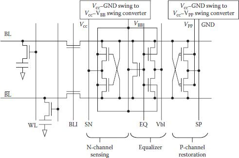
FIGURE 8.13
Well synchronized sensing/equalizing structure. (Adapted from “A Well-Synchronized Sensing/Equalizing Method for Sub-1.0 V Operating Advanced DRAMs,” Ooishi et al., Symp. VLSI Circuit Tech. Papers, pp. 81–82, 1993.)
With DRAM density increasing beyond 4 Mbit/16 Mbit range, capacitance of the bit line increases even when a small part of it is activated (division of bit line is limited by the assembly technology on chip) and writing resistance from sense amplifier driving node to ground also increases in spite of using resistance reducing techniques. This larger characteristic time constant of the bit line necessitates much longer time for its signal development. Moreover, as large discharge current flows through the bit line and the sense amplifier driving transistor at the time of turning it on, large voltage drop takes place clamping sense amplifier driving node at nearly ground level and reducing effective gate-to-source voltage. In addition, sometimes there is a weak column, where for some reason initial sensing signal is smaller than for a normal column. In the weak column, signal development is very slow, which becomes a serious problem in high-density DRAM. A decoded source sense amplifier (DSSA) sensing is shown in Figure 8.14 that solves the two problems mentioned through decoding of each source and connecting it to the sense amplifier driving node through the use of two additional transistors Qn1 and Qn2 only [23].
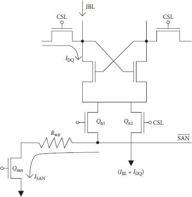
FIGURE 8.14
Sensing scheme of the decoded source sense amplifier showing only a selected column. (Redrawn from “Decoded-Source Sense Amplifier for High-Density DRAM’s,” J Okamura et al., IEEE J. of Solid State Circuits, Vol. 25, pp. 18–23, 1990.)
With the requirement of low voltage application, especially in mobile equipment employing multimedia systems, the sense signal from the memory cell became very small. It was reaching near the sense amplifier limits. The charge transfer sense amplifier technique of Section 8.4.2 which tried to overcome the limitation through preamplification was using full supply voltage precharging of the bit lines. However, with the established advantages of half-VCC precharging it became imperative to apply it with the charge transfer sensing and Tsukude and others presented such a scheme in 1997 [24]. Earlier schemes of Heller [15,16] could not be directly applied with half-VCC precharging as it required an excessively high sense amplifier precharge level (VSAP). Principle of the proposed charge transfer presenting scheme (CTPS) is shown in Figure 8.15(a), where the transistor TG isolates the SA and the bit line and transfers the stored charge from the bit line to the SA node. As in the earlier charge transfer schemes, stored charge is first transferred to the bit line and then to the SA node. Utilization of the half-VDD bit line precharging CTPS with SA circuit arrangement for a DRAM cell is shown in Figure 8.15(b). For a 0.8 V array operation, bit line was precharged to 0.4 V and SA node was precharged to 1.6 V to satisfy the charge transfer voltage level conditions. During read/refresh operation, gate voltage of TG is to be selected for its proper operating node to transfer charge from bit line to SA node. As before, the whole operation is divided into charge transfer state and sensing state and is once again ready for the next precharging. A five times larger sense signal was easily obtained compared to the conventional sensing scheme and data transfer and sensing speed increased by 40% in 0.8 V array operation without the requirement of reduced threshold voltage in sense amplifier [24].
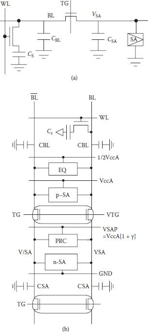
FIGURE 8.15
(a) Arrangement of charge transfer pre-sensing with 1/2Vcc BL-precharge. (Redrawn from “A 1.2 V to 3.3 V Wide Voltage-Range/Low-Power DRAM with a Charge-Transfer Presenting Scheme,” M. Tsukude et al., IEEE J. of Solid-State Circuits, Vol. 32, pp. 1721–1727, 1997.) (b) Circuit organization of CTPS with 1/2Vcc BL precharge at VccA = 0.8 V. (“A 1.2 V to 3.3 V Wide Voltage-Range/Low-Power DRAM with a Charge-Transfer Presenting Scheme,” M. Tsukude et al., IEEE J. of Solid-State Circuits, Vol. 32, pp. 1721–1727, 1997.)
Well-synchronized sensing was used to suppress body effect in SA transistor, but it suffered from noise generation because of forward biasing between the bit line and the well before sensing. In a modified charge-transfer well sensing scheme, the problem was considerably reduced by having well potential less than half-VDD [25]. Moreover, in this scheme the well under SA was not charged from the power supply, hence there was no power loss compared to the earlier well sensing [22] scheme. However, latching delay is larger than 10 ns in charge transfer well-sensing, which is not suitable for high-speed applications.
Overdriving of the access transistor has been used quite effectively in DRAM cells. Overdriving of the SA has also been used by connecting external VDD to it to enhance the data sensing speed while a lower internal array voltage is applied to maintain the stored voltage [26]. Sometimes initial voltage to the SA is greater than VDD also, though for short duration, but it sends larger current creating difficulty in power supply design. Another low-voltage sense amplifier driver scheme was proposed to work at supply voltage below 0.9 V and was able to give higher speed using SA overdriving [27] using boost capacitors. Bit line was temporarily isolated from sense amplifier to reduce the capacitive load of the sense amplifier so as to reduce the column switching time. Though the isolation transistor drivers and the boost capacitor driver consume extra power, it was reduced using charge recycle technique. Bit line isolator (BI) transistors were temporarily closed during data sensing to reduce capacitive load on SA. For VCC = 0.9 V, capacitors provided Vpp (= 1.8 VCC) which drives BI and VCC/2–precharge transistors. To reduce the power consumption, charge recycling effected a 28% reduction compared to the case without charge recycling, though overall power consumption was still more than 50% compared to conventional SA drivers [27]. It is not only the overdriving but also the method of overdriving of SA that is important for reducing the duration of sensing; Table 8.1 shows such a comparison. Higher density DRAM shall have impractically large sensing duration at reduced array voltage of 1.0 V or below, whereas conventional overdriving does not provide satisfactory performance. A distributed driver scheme along with meshed power line has shown improvement of 2.0 ns and 7.0 ns for 1 Gbit DRAM at 1.2 V of array voltage over a conventionally over-driven and non-overdriven SA [28].
Comparison of Sensing Duration for Non-Overdriven and Overdriven SAs in Nanoseconds
Bit Line Swing (Volts) |
DRAM Density, Technology Node (μm) |
Conventional Non-Overdriven |
Conventional Overdriven |
Distributed Overdriven Scheme [28] |
1.8 |
256 Mb (0.18) |
5.6 |
4.8 |
3.0 |
1.6 |
256 Mb (0.18) 1 Gb (0.13) |
6.2 |
4.9 |
3.2 |
1.4 |
1 Gb (0.13) |
7.9 |
5.6 |
3.6 |
1.2 |
1 Gb (0.13) 4 Gb (0.09) |
11.0 |
6.0 |
4.0 |
1.0 |
4 Gb (0.09) |
Impractical |
7.4 |
5.2 |
0.8 |
4 Gb (0.09) |
Impractical |
11.5 |
7.4 |
8.4.3 Threshold-Voltage Mismatch Compensated Sense Amplifiers
With increased DRAM density, number of SAs also increased, occupying larger chip area as core of the SAs consisted of pairs of NMOS and PMOS transistors. Apart from the large number of SAs, use of planar transistors increases total chip area occupied. Advanced transistor structures, which are used in DRAM cores, are generally not used in sense amplifiers. Efforts are always on to see that overheads because of SAs are restricted, but a more serious problem encountered in the SAs is the generation of offset, forcing a minimum required sense signal. The difference between the sensing signal and offset voltage is critical as it affects the duration of signal restoration by the SA and DRAM cell refreshing period as well. Reasons for the generation of offset are different and the components responsible for it change their weightage at different density levels and the technologies used, as will be shown later, but one of the most significant reasons is the threshold voltage (Vth) mismatch between transistor pairs of the SAs. Even with the most advanced technology, threshold mismatch (ΔVth) is unavoidable, though it is reducible, obviously at a higher manufacturing cost. It is, therefore, very important to use compensation/cancellation of the effect of ΔVth, to have stable operation of the SAs. The problem was identified early and circuit techniques for Vth compensation were initiated even in 1979 [29]. The basic idea in such techniques was to change either gate voltage [29] or source voltage [30] to set gate source voltage in the transistor pairs equal to their own threshold voltage before reading the signal from a cell. Hierarchical data line architecture with direct sensing scheme was given by Kawahara et al. for Vth mismatch compensation in SAs along with reducing their area as well [31]. Figure 8.16 shows given Vth compensation scheme, where D and is the sub-data-line pair which is different from global-data-line. Pair of transistors MT1 and MT2 is used for Vth compensation of the signal detection transistors M1 and M2. When transistors MT1 and MT2 are made on, these are converted as diodes for M1 and M2 while discharging data line capacitance corresponding to a level at its own Vth [31]. Normally, Vth1 is higher (lower) than Vth2 by ΔVth, which needed cancellation. In this scheme, voltage in line D is set higher than by ΔVth when control pulse is on. Hence, original ΔVth between M1 and M2 is cancelled.
FIGURE 8.16
Schematic of sense amplifier operation ∆Vth compensation. (Redrawn from“A High-Speed, Small-Area, Threshold-Voltage-Mismatch Compensation Sense Amplifier for Gigabit-Scale DRAM arrays,” T. Kawahara et al., IEEE J. Solid-State Circuits, Vol. 28, pp. 816–823, 1993.)
Bit line direct sensing schemes have the advantage of fast signal development in comparison to the conventional cross-coupled sense amplifiers since they do not require any dynamic timing margin. However, static amplifiers require offset/imbalance compensation to maintain sensitivity. Several schemes have been given for compensating imbalance in dynamic cross-coupled SAs, which generally used bit line precharge level adjustment for the purpose [32,33]. To overcome their common drawback of slower operating speed, a direct bit line sensing scheme using a current mirror differential amplifier was proposed in 1999 [34], as shown in Figure 8.17. Thicker lines show the circuit part, which is used for read operation for the offset compensation scheme (OCS) in a simplified bit line SA. Switching is used in such a way that BL is automatically precharged to a level that compensates the offset, though accuracy of level shifting of BL also depends on the finite gain of the differential amplifier. The scheme worked satisfactorily at around 256 KB DRAM density level, but it could not be applied for manufacturing because of the large size of the compensating circuit, which could not fit in the pitch. A similar scheme was given by S. Hong and others which improved the data retention time of DRAM by nearly 2.4 times at an operating voltage of 1.5 V and reduced required number of SAs as each SA supported larger number of cells [35]. Figure 8.18 shows the basic offset cancellation sense amplifier (OCSA) circuit. Normal read operation begins with VDD/2 precharging, but simultaneously offset is canceled by forming current mirror on left-hand side and the sensed signal is allowed to develop with word line raised. After slight signal development, modification takes place in the form of signal locking using positive feedback with only M8 on. Slightly enhanced bit line signal at the lock stage is able to overcome any remaining offset and signal restoration follows in usual manner.
FIGURE 8.17
Schematic diagram of the OCS circuit. (Redrawn from “Offset Compensating Bit-Line Sensing Scheme for High Density DRAM’s,” Y. Watanabe, N. Nakamura and S. Watanabe, IEEE J. Solid-State Circuits, Vol. 29, pp. 9–13, 1994.)
FIGURE 8.18
Offset-cancelation sense amplifier. (Redrawn from “Low-Voltage DRAM Sensing Scheme with Offset-Cancellation Sense Amplifier,” S. Hong et al., IEEE J. Solid-State Circuits, Vol. 37, pp. 1356–1360, 2002.)
The problem of having a differential amplifier and use of quite a few control switches, which could not be easily fabricated within a single pitch of a SA, still remained in the discussed schemes. Moreover, large current drawn by the differential amplifiers and delay caused by the offset cancellation process before activation of WL were the other drawbacks. Complication further arose because of the continued reduction in the DRAM core operating voltage, especially for mobile applications. For low voltages multistage amplification became imperative even with direct sensing. At the same time VCC/2 precharge scheme even at low voltage was desirable, which necessitated the application of boosted voltage for bit line equalization. However, generation of boosted voltage required larger current for pump circuits. An offset compensated presensing (OCPS) scheme has been given which retains only BL and nodes in an SA pitch. Switching arrangement has also been simplified by using two separated amplifiers and only one of them provides offset cancellation at a time [36]. A charge recycle precharge (CRP) scheme was also employed where core voltage was 1.0 V, boosted bit-line equalization voltage was 1.2 V, and WL voltage was 2.7 V. Overall chip size overhead due to the use of OCPS was 3% and at VCC = 1.0 V, access time of 25 ns could be achieved.
8.4.4 Low-Voltage Charge-Transferred Presensing
Due to the nonscalable nature of the threshold voltage of the access transistor, its drivability is reduced at low DRAM core voltage. For any up-voltage conversion, pumping circuits consume power. Available charge-transferred presenting schemes (CTPS) [15,16,24] did improve performance at low voltage but suffered from constraints. Biasing should be within close limits so that isolation transistor(s) remain in saturation, and ratio of storage capacitance with bit line capacitance also affects the operating mode of the isolation transistor. A new scheme eliminates any constraint on the bias levels of the conventional CTPS [37]. Figure 8.19 shows basics of the proposed CTPS scheme. Transistor N7 and N8 are turned on after the initial charge sharing phase, which allows initial presenting on account of capacitance difference between CBL and CSBL. Regenerative action due to positive feedback in the transistor N9 network takes place. Normal sensing by P1 and P2 follows, which is preceded by the pulling down of one of the bit lines. Presence of positive feedback eliminates any chance of polarity change between SBL and SBLB. If the threshold voltage of the access transistor is less than half of array supply voltage, then there is no constraint on bias voltage for circuit reliability [37]. In conventional CTPS schemes BL flipping can occur if column line is selected early during the sensing process; therefore, to avoid it, selection of column line is delayed by about 3 ns. In the proposed scheme, presence of positive feedback resulted in the sensing of this time delay at array voltage of 1.3 V, without any time delay.
FIGURE 8.19
Circuit diagram of the charge transfer presenting scheme (CTPS). (Redrawn from “Charge-Transferred Presenting, Negatively Precharged Word-Line, and Temperature-Insensitive-Up Schemes for Low-Voltage DRAMs,” J.Y. Sim et al., IEEE J. Solid-State Circuits, Vol. 39, pp. 694–703, 2004.)
Trends for DRAM supply voltage indicated it to be reduced to 1.0 V by 2010; therefore working with data line voltage of 0.5 V was becoming essential [38]. At this reduced voltage, sense signal available from bit lines is very near to the sensing limit and sensing speed also becomes slow. Charge transfer schemes tried to overcome this problem, as discussed earlier, at a relatively larger voltage. A boosted charged transfer preamplifier scheme (BCTP) tried to solve the problem for a 0.5 V DRAM and aimed to provide higher speed as well [39]. However, some fine reports by Hitachi have served well in this direction [40, 41, 42 and 43], and Figure 8.20 shows the development. First among such schemes in Figure 8.20 (without the block in dotted lines) is a low Vth gated preamplifier (LGA) in parallel with a conventional high Vth SA. Because of the low value of Vth in the LGA, it quickly amplifies the small bit line differential signal (vso) even with VDD/2 array precharging. The amplification is achieved by turning transistors M7 and M8 on though SG and bit line differential voltage value is reached above the offset voltage of the high Vth SA (vs1). Full restoration of voltage level is done by the high Vth conventional SA and the SG level turns off the low Vth preamplifier to reduce leakage. At 70 nm technology a 128 Mbit DRAM was fabricated using LGA which has a read access time of 14.3 ns at read current of 75 mA and row access time of 16.4 ns at an array voltage of 0.9 V. Application of LGA for gigabit DRAMs had certain limitations. For example, threshold voltage of the high-Vth NMOS should be less than 0.61 V and threshold voltage of the high Vth PMOS should be greater than −0.64 V so that leakage current does not increase above 100 μA for 128 SAs. Secondly, with data line voltage at 0.5 V, and with optimum threshold voltage of low Vth NMOS of 0.3 V, achievable minimum sensing time ts is 15.6 ns. One of the reasons ts could not be reduced was the voltage drop at the high-level data line (ΔVH) as it increased the total charge supplied for the data line by high Vth PMOS.
FIGURE 8.20
(a) Schematic diagram of a sense amplifier having low VT preamplifier and high VT CMOS latch (SANP), modified to CPA and for asymmetrical cross-coupled SA (ASA). (b) Operational sequence of the SANP. (“Asymmetric Cross-Coupled Sense Amplifier for Small-Sized 0.5 V Gigabit-DRAM Arrays,” A. Kotabe et al., IEEE Asin S.S. Circ. Conf., 2010.)
To improve upon the LGA, a CMOS low Vth preamplifier (CPA) was developed in which low Vth PMOS cross couple (M9, M10) and PMOSs (M11, M12) are added to it as shown in Figure 8.20 (block in dotted line now included) [41,42]. To achieve both better speed and data sensing with low power, a low-Vth (NMOS and PMOS) activation scheme was used in which both old and newly added preamplifiers get activated simultaneously. It results in reduced value of ΔVH, thereby increasing the sensing speed. The rest of the operation is similar to the LGA. In this scheme sensing time was reduced to 6 ns (62% shorter than for LGA) and writing time was reduced to 16.3 s (72% less than a high Vth CMOS latch only). Data line charging current also reduced by 26% with decreases in data line voltage from 0.8 V to 0.5 V.
Addition of low Vth PMOS preamplifier improved the operation, but it also increased chip area; an overall increase of 9% for 128 Mbit bank. Hence, further modification was done in which two cross couples of CPA are eliminated which not only reduced required area but provided faster operation as well as low data leakage [43]. However, the modified simpler structure, as such, called asymmetric cross-coupled SA (ASA) was slow in sensing and writing due to high Vth PMOS latch and large leakage from low Vth NMOS preamplifier. The problem was solved by using an overdrive of common source (SP) and reduction in the threshold of PMOS. Power dissipation increased due to increased overdrive voltage, hence a new overdrive of the high Vth PMOS with transfer-gate clocking is used which sped sense and restore operations. An adaptive leakage control of the preamplifier was also used to considerably reduce leakage and maintain safe limits. Figure 8.20 shows the structure (all components shown with thick lines deleted) of a column circuit using ASA for high-speed operation and small leakage in active standby mode.
8.5 Error Checking and Correction
Alpha particle-induced soft error is a serious problem in high-density DRAMs. Apart from steps taken for its prevention, error checking and correction (ECC) circuits are extremely important. A 4 Mbit DRAM fabricated in 0.8 μm CMOS technology has employed concurrent 16-bit ECC(C-ECC) along with duplex bit line architecture (DBA) [44]. The DBA architecture provides multiple bit internal operations and with C-ECC multiple-bit error checking and correction could become possible without expanding memory.
In the conventional bidirectional parity code method, vertical and horizontal cell data are processed and checked [45]. However, method becomes complex for multiple data output. On the other hand, in C-ECC, all V-directional data is checked concurrently with simplified process [44]. The C-ECC consumes less chip area (~7.5% of whole area) than the conventional ECC. Improvement of nearly 1010 was obtained in the soft error rate (SER) in the 16-bit concurrent ECC.
Other than the horizontal/vertical (HV) parity code, built-in ECC circuits also use Hamming code. The Hamming code circuit checks all data bits on an ECC data group simultaneously. Therefore, it has higher error-correcting frequency and provides better reliability. Built-in circuits can use formation of ECC data groups through subarrays. For example, a 256 Kbit DRAM used a short ECC code with eight data bits and four check bits [46]. In a similar scheme, an HV parity ECC data group is formed with data associated with an identical word line in a subarray. Parity checker monitors both horizontal and vertical groups where selected data resides.
Though chip area used is less than first scheme, it incurs a penalty of 5 ns in access time [47]. Limitations of larger chip area consumption or access time delay in different implementations are improved in another Hamming code ECC technique using eight data bits and four check bits. ECC data group is formed with cells that are selected by an identical word line and single error bit is found by calculating the syndrome S using parity checker matrix [48]. The built-in Hamming code ECC combined with redundancy could reduce SER about 100 times less than using HV parity code ECC.
8.6 On-Chip Redundancy Techniques and ECC
As early as 1967, spare rows were used to replace defective ones to get improved yield and enhanced reliability [49]. Soon spare columns were also used along with spare rows [50]. A separate area was allocated to accommodate spare word lines, bit lines, decoders, and a few additional reset lines as shown in Figure 8.21. Decoders in the separate area are different and have two output states. In one state the decoder does not respond to any address, but in the second state an address can be attributed to it, which is the address of the faulty row/column being replaced. However, it is extremely important to find the faulty row/column correctly and get it replaced by the spare line quickly. Different approaches have been used for storing the information about the faulty lines and for the implementation of the redundancy.
FIGURE 8.21
Spare word lines, bit lines, and decoders for improving yield. (Redrawn from “Multiple Word/Bit line Redundancy for Semiconductor Memories,” S.E. Schuster, IEEE. J. Solid State Circuits, Vol. SC-13, pp. 698–703, 1978.)
In the initial level analysis, it was observed that faulty bits were either due to gross imperfections or due to random defects in the photolithography, processing, and materials [51]. Random defects were further classified as (1) in the correctable area where a cell or word/bit line only was faulty and it could be replaced by the spare line, and (2) in an uncorrectable part due to which most of the chip fails. Uncorrectable or fatal defects can occur in supply lines, clock wires, or address lines. Obviously chip productivity highly depends on uncorrectable defect-susceptible area. In a typical example, for a four-critical-defects-per-4-Kbit array, effective yield was shown to be less than 2%. However, it increased to more than 70% with the addition of seven word and seven bit spare lines [51].
Laser fusing redundancy circuits have been used in many applications for improving yield without speed degradation and with minimum number of links [52], but fusing involved a mechanically difficult process. Alternatively an increase in the number of spare word/bit lines has been used to reduce the required number of fuses, which occupied as much as 25% of the array area [53]. Comparatively fewer spare rows and column lines have been used while increasing yield five times and requiring fewer number of fuses to be blown [54]. In this report spare memory cells form two logical groups of four rows and two groups of two spare columns. This array architecture provided maximum efficiency in removing random defects. Laser-blown polysilicon fuses have been used at 1 Mbit DRAM density level, which could provide 81% repairable die area through redundancy [55].
Use of redundant circuits and ECC was implemented on a 50 ns 16 Mbit DRAM providing excellent fault tolerance [56]. The 16 Mbit chip was divided in four independent quadrants, each one having its bit redundancy and data steering, word redundancy system, ECC circuitry, and SRAM. Each quadrant contained four array blocks with 1024 word lines. Each WL contained eight ECC words, where each word had 128 data bits and 9 check bits. With 16 bits for the redundant bit lines, combined with 8 ECC words each word line comprised of 1112 bits.
An optimum odd-weight Hamming code was used with 128 data bits and 9 check bits [57] for double-error detection/single-error correction. Single cell error could be effectively corrected using the ECC circuit, but, for more than one bit failure, correction needed redundancy circuits. For 64 data blocks, each contained 2048 ECC words and two redundant bit lines. Combined effect of ECC and redundant circuits showed dramatic improvements. To obtain an expected yield of 50%, without the use of ECC circuits, no more than 28 random single bit failures were allowed, whereas the number of permissible failures increased to 428 and 2725, respectively, for the two cases when only ECC was used and when ECC was combined with redundancy circuits.
8.7 Redundancy Schemes for High-Density DRAMs
Use of spare column and bit lines was very effective in yield and reliability improvement up to 64–256 Kbit DRAM range, though the simple arrangement faced a few constraints:
1. Degradation in raw yield forced deployment of larger numbers of spare row/column lines and spare decoders. Resultant chip area overhead became excessively large.
2. Defects/faults in the redundancy overhead area also became significant.
3. With increase in DRAM density, memory array division started both without and with hierarchical word line. Arrangement of redundancy which worked in single core became prohibitively large in multi-divided array.
4. Because of the connecting wire strips becoming thin with increased DRAM density, chances of lines open circuiting or short circuiting with the supply or ground lines increased. It caused DC characteristic faults, especially increase in the standby current (ISB) fault.
It became necessary to improve redundancy techniques without which the main advantage of the DRAM, lowest cost per bit, was likely to be under threat. In early stages of DRAM production, an estimation of yield was as given in Table 8.2 [4]. It was based on the assumed effective defect density D of 2/cm2 [58] and increase of chip area 1.5× with each DRAM generation. Out of the total chip area, memory cells, decoders, word drivers, and sense amplifiers were assumed to take up nearly 80% and the remaining area was left for the other peripherals. It was observed that the then used spare line redundancy resulted in only about half of the yield at 256 Mbit level compared to that at 16 Mbit level of DRAMs.
Estimated Yield Improvement Range through Line and Subarray Replacement with D = 2/Cm2 and Chip Area 1.5× per Generation
DRAM density |
16 Mb |
64 Mb |
256 Mb |
1 Gb |
Yield (%) |
||||
Without redundancy |
12–6 |
6–~1% |
nil |
nil |
Line replacement |
62–50 |
50–37 |
37–25 |
25–10 |
Subarray replacement |
82–75 |
75–65 |
65–55 |
55–40 |
8.7.1 Subarray Replacement Redundancy for ISB Faults
Yield of gigabit DRAMs is mainly affected by DC characteristic faults, like short circuit between a word line (at ground level during standby) and a bit line (precharge voltage-VCC/2) causing flow of excessively large standby current (ISB). Replacement of defective word/bit line will remove the fault, but large ISB current would continue to flow, which needs to be minimized/stopped. In one scheme ISB was limited to ~15 μA/short circuit using a current limiter through the precharge supply line [59].
In a similar approach DC current is cut off by a power switch controlled by a fuse [60]. However, a preferred scheme is given by Kitsukawa and others for ISB fault correction through on-chip replacement of a defective subarray [4]. Figure 8.22 shows an example of an ISB fault where bit line at precharge voltage (VCC/2) is shown to be short circuited with the grounded word line, and also shows a subarray replacement scheme for its correction. For implementing the scheme, each subarray contains power switches for the precharge voltage (VCC/2) and the cell plate voltage VPL. The subarray also needs timing signal and a fuse ROM to control the time signal gate. Power switches of the defective subarray are turned off and those for the spare array are turned on; hence, the faulty ISB current path is cut off. With the increase in the number of subarrays in high-density DRAMs, the scheme finds favor.
FIGURE 8.22
Subarray having ISB fault replacement redundancy technique. (Redrawn from “256 Mb DRAM Circuit Technologies for File Applications,” G. Kitsukawa et al., IEEE J.S.C. Circuits, Vol. 28, pp. 1105–1113, 1993.)
8.7.2 Flexible Redundancy Technique
In conventional redundancy applications in DRAMs without cell array division, defective word line addresses are programmed in the address comparators (ACs) and compared with the input address. The number of comparators is equal to the number of spare word lines (say L); hence, only L defective word lines can be replaced [54,61]. With increasing DRAM density the cell array is divided many times (M); then inter-subarray (SAR) replacement, in which defective line in one array should not be replaced by spare line in another SAR as it increases memory array control complexity considerably. The following two approaches have been suggested [58]:
1. Simultaneous replacement scheme in which ACs equal L in a subarray and each AC compares only the intra-SAR address signals and output is sent to all SARs. This means that to replace one defective line (L-1), other functional lines with the same intra-SAR address are also replaced. Hence, it requires a larger number of spare lines increasing wasteful chip area, and the possibility of a defect in the spare line, which is replacing a faulty line, also increases.
2. In a similar scheme, called individual replacement, every spare line in each SAR has its own ACs. Therefore, the number of ACs increases and equals the product L*M, but has some advantages over scheme 1. above. Statistically, required value of L for as many defects becomes small and only one line is replaced by the spare line, avoiding wasteful chip area. However, more area is taken up by the ACs.
Problems and limitations in the two schemes were minimized in a flexible intra-SAR replacement scheme [58]. The ACs are connected to the spare lines through OR gates, so that each AC compares both intra-and inter-SAR address signals. This kind of arrangement provides flexibility between ACs and spare lines, where one spare line can be reached by several ACs; hence, the number of ACs required (C) is also flexible as per the relationship L ≤ C ≤ L*M/m, where m is the number of SARs in which spare lines replace faulty lines simultaneously. It was observed that the flexible redundancy technique was more effective at higher density where the yield became mainly dependent on fatal defects discussed in Section 8.7.1.
8.7.3 Inter-Subarray Replacement Redundancy
For high-density DRAMs chances of clustered defects increase. For such repairs in intra-SAR replacement techniques, required spare lines L in a SAR must be more than or equal to the defective lines, which means larger value for L or larger chip overhead.
At least two inter-SAR replacement redundancy techniques shown in Figure 8.23 have been employed in which defective lines could be repaired by the spare line in any SAR. In the distributed-spare line approach, shown in Figure 8.23(a), each SAR has spare line, but these lines can replace a faulty line in any other SAR as well. Hence, a cluster of L*M defects can be repaired in any SAR, with L being the average number of defective lines (not maximum) in a SAR. Number of ACs equals L*M, though it can be reduced a bit [62].
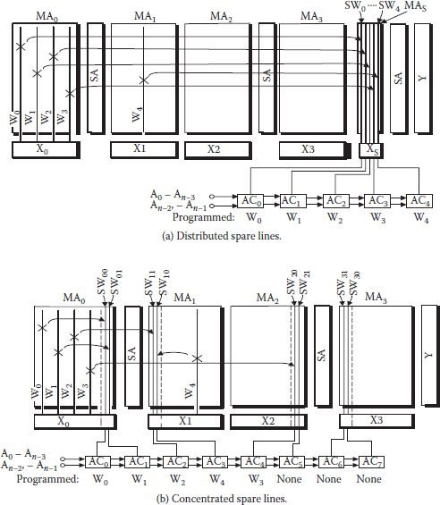
FIGURE 8.23
Inter-subarray replacement redundancy techniques. (“Redundancy Techniques for High-Density RAMs,” M. Horiguchi et al., Int. Conf. Innovative Systems in Silicon, pp. 22–29, 1997.)
Concentrated-spare line approach shown in Figure 8.23(b) is based on a separate SAR whose lines are used as spare lines and can replace any defective line [59,63]. The remaining SARs do not have any spare lines. Number of lines in the spare SAR is flexible (L′); obviously, L′ defects clustered anywhere can be rectified. The number of ACs used equal L′ and since the L′ number is flexible, use of comparators becomes economical. However, a separate SAR needs an extra decoder, sense amplifier, and so on. Access time penalty is also a little more than intra-SAR replacement technique because an activated SAR may be changed as per requirement instead of an activated line only.
8.7.4 DRAM Architecture–Based Redundancy Techniques
Redundancy area unit (RAU) is a memory area comprising either rows or columns that can be repaired, if faulty, by a single spare line. Obvious a system having larger RAU needs fewer spare lines. At higher DRAM density level, multibank architecture is now common, but because of more than one bank being active simultaneously, spare elements cannot be shared. More spares are now required, forcing RAU to be small, even when all spare lines in a bank might not be used. Since high-speed multibit column access is needed, a defect replacement from a spare line located at a large distance physically adds to the access delay which is another reason for having smaller RAU in DRAMs. Flexible redundancy technique of Section 8.7.2 did introduce a flexible relation between fuse set and spare element, but it was subjected to certain constraints and chip area efficiency was less, which was improved in another technique called flexible mapping redundancy (FMR) [64]. The main feature of the scheme is that instead of maintaining an equal number of spare lines and fuse sets with one-to-one correspondence between them, a different approach is adopted. In a flexible correspondence, which is obtained by mapping fuses in a fuse set, numbers of fuse sets that store the addresses of the defects are less than the numbers of spare elements. The mapping data that are stored in a fuse set are based on the defect distribution information. Both row and column redundancies are effectively used. For a 16-bank DRAM, 13% of chip area saving was obtained in comparison to a conventional scheme and the total area occupied by the FMR scheme was 5.2% of the chip.
For increasing bandwidth, DRAMs often used an architecture having hierarchical data lines with multiple I/Os [65]. In such structures column redundancy acquires greater importance [66]. A flexible column redundancy circuit for such architecture has been reported involving I/O shifting [67]. Fuse mapping algorithm use minimizes redundancy circuit overhead. Proposed flexible column redundancy circuit has RAU containing eight segments and two redundant segments at each end of the eight segments. In each of the eight segments there are 64 column select lines (CSLs) and four I/O pairs and each redundant column has four redundant CSLs and four I/O pairs. The scheme works in such a way that a maximum of eight columns can be repaired for eight segments. A control circuit for shift switches and the mapping table was also given which determines the state of the switches. Number of fuses used in the scheme was fewer than those used in the FMR scheme [64] mentioned above.
A dual CSL column redundancy scheme (DCCR) has two symmetrical I/O buses in one I/O block, which translates into an action in which one CSL and one spare column line selection (SCSL) can be activated simultaneously on repairing access. Hence, in high-speed DRAMs with multiple bit prefetch structures, the proposed scheme repairs defective bits by single units [68]. In a four-bit prefetch, RAU of the DCCR becomes as large as eight times compared to a conventional column redundancy scheme. From this brief discussion in this section, it is obvious that architecture of the DRAM has great influence on the method of application of redundancy, and needs to be pursued for future benefits.
1. J.M. Rabaey, A. Chandrakasan, and B. Nikalic, Digital Integrated Circuits—A Design Perspective, Pearson Edition, 2003.
2. R. J.C. Chwang et al., “A 70 ns High Density 64 K CMOS Dynamic RAM,” IEEE J.S.S. Circuits, Vol. SC-18, pp. 457–463, 1983.
3. K. Kimura et al., “Power Reduction Techniques in Megabit DRAM’s,” IEEE J.S.S. Circuits, Vol. SC-21, pp. 382–388, 1986.
4. G. Kitsukawa et al., “256 Mb DRAM Circuit Technologies for File Applications,” IEEE J.S.C. Circuits, Vol. 28, pp. 1105–1113, 1993.
5. J.J. Barnes et al., “Circuit Techniques for a 25 ns 16 K x 1 SRAM Using Address-Transition Detection,” IEEE J.S.C. Circuits, Vol. SC-19, pp. 455–461, 1984.
6. L.F. Childs and R.T. Hirase, “A 18 ns 4K x 4 CMOS SRAM,” IEEE J.S.S. Circuits, Vol. SC-19, pp. 454–551, 1984.
7. H. Nimbu et al., “A 1.8 ns Access, 550 MHz 4.5 Mb CMOS SRAM,” Proc. ISS. CC. Dig. Tech. Papers, paper SP 22.7, 1998.
8. F. Baba et al. “A 64 K DRAM with 35 ns Static Column Operation,” IEEE J.S.S. Circuits, Vol. SC-18, pp. 447–451, 1983.
9. R.T. Taylor and M.G. Johnson, “A 1-Mbit CMOS Dynamic RAM with a Divided Bit Line Matrix Architecture,” IEEE J.S.S. Circuits, Vol. SC-20, pp. 894–902, 1985.
10. K.U. Stein et al., “Storage Array and Sense/Refresh Circuit for Single Transistor Memory Cell, “ IEEE J. of Solid State Circuits, Vol. SC-7, pp. 336–340, 1972.
11. C. Kuo et al., “Sense Amplifier Design Is Key to the One-Transistor Cell in 4096 Bit RAM,” Electronics, Vol. 46, pp. 116–121, 1973.
12. R.C. Foss and R. Harland, “Peripheral Circuits for One-Transistor Cell MOS RAM’s,” IEEE J. of Solid State Circuits, Vol. SC-10, pp. 225–261, 1975.
13. C.N. Ahlquist et al., “A 16384-Bit Dynamic RAM,” IEEE J. of Solid State Circuits, Vol. SC-11, no. 5, pp. 570–574, 1976.
14. W.T. Lynch and H.J. Boll, “Optimization of the Latching Pulse for Dynamic Flip-Flop Sensors,” IEEE J. of Solid State Circuits, Vol. SC-9, pp. 49–55, 1974.
15. L.G. Heller et al., “High-Sensitivity Charge-Transfer Sense Amplifier,” IEEE J. of Solid-State Circuits, Vol. SC-11, pp. 596–601, 1976.
16. L.G. Heller, “Cross-Coupled Charge-Transfer Sense Amplifier,” IEEE, ISSCC. Digest of Tech. Papers, pp. 20–21, 1979.
17. N.C.C. Lu and H.H. Chao, “Half-VDD Bit-Line Sensing Schemes in CMOS DRAMs,” IEEE J. of Solid State Circuits, Vol. SC-19, pp. 451–454, 1984.
18. S. Fujii et al., “A 50 μA Standby 1 Mx 1/256 x 4 CMOS DRAM,” IEEE J. of Solid State Circuits, Vol. SC-21, pp. 627–634, 1986.
19. T. Mano et al., “Circuit Techniques for 16 Mb DRAMs,” ISSCC Dig. Tech. Papers, pp. 22–23, Feb. 1987.
20. D. Chin and W. Hwang, “Quarter-VDD Sensing Schemes in CMOS DRAMs,” IBM Tech. Disc. Bull., pp. 3750–3751, Jan. 1987.
21. S.H. Dhong et al., “High-Speed Sensing Scheme for CMOS DRAMs,” IEEE J. of Solid State Circuits, Vol. 23, pp. 34–40, 1988.
22. T. Ooishi et al., “A Well-Synchronized Sensing/Equalizing Method for Sub-1.0 V Operating Advanced DRAMs,” Symp. VLSI Circuit Tech. Papers, pp. 81–82, 1993.
23. J. Okamura et al., “Decoded-Source Sense Amplifier for High-Density DRAM’s,” IEEE J. of Solid State Circuits, Vol. 25, pp. 18–23, 1990.
24. M. Tsukude et al., “A 1.2 V to 3.3 V Wide Voltage-Range/Low-Power DRAM with a Charge-Transfer Presenting Scheme,” IEEE J. of Solid State Circuits, Vol. 32, pp. 1721–1727, 1997.
25. T. Yamagata et al., “Circuit Design Techniques for Low-Voltage Operating and/or Giga-Scale DRAMs,” ISSCC, Dig. of Tech. Papers, pp. 113–114, 1995.
26. M. Nakamura et al., “A 29 ns 64 MB DRAM with Hierarchical Array Architecture,” ISSCC, Dig. of Tech. Papers, pp. 246–247, 1995.
27. K. Gotoh et al., “A 0.9 V Sense-Amplifier Driver for High-Speed Gb-Scale DRAMs,” IEEE Symp. VLSI Circuits, Dig. of Tech. Papers, pp. 108–109, 1996.
28. T. Takashahi et al., “A Multi-Gigabit DRAM Technology with 6 F2 Open-Bit-Line Cell Distributed Over-Driven Sensing and Stacked-Flash Fuse,” IEEE Intern. S.S. Circ. Conf., pp. 465–468, 2001.
29. S. Suzuki et al., “Threshold Difference Compensated Sense Amplifier,” IEEE J. Solid State Circuits, Vol. SC-14, pp. 1066–1070, 1979.
30. T. Mano et al., “Submicron VLSI Memory Circuit,” ISSCC Dig. Tech. Papers, pp. 234–235, 1983.
31. T. Kawahara et al., “A High-Speed, Small-Area, Threshold-Voltage-Mismatch Compensation Sense Amplifier for Gigabit-Scale DRAM Arrays,” IEEE J. Solid State Circuits, Vol. 28, pp. 816–823, 1993.
32. S. Suzuki and M. Hirata, “Threshold Difference Compensated Sense Amplifier,” IEEE J. Solid State Circuits, Vol. SC-15, pp. 1066–1070, 1979.
33. T. Furuyama, S. Saito, and S. Fuiji, “A New Sense Amplifier Technique for VLSI Dynamic RAM’s,” IEDM Tech. Dig., pp. 44–47, 1981.
34. Y. Watanabe, N. Nakamura, and S. Watanabe, “Offset Compensating Bit-Line Sensing Scheme for High Density DRAM’s,” IEEE J. Solid State Circuits, Vol. 29, pp. 9–13, 1994.
35. S. Hong et al., “Low-Voltage DRAM Sensing Scheme with Offset-Cancellation Sense Amplifier,” IEEE J. Solid State Circuits, Vol. 37, pp. 1356–1360, 2002.
36. J.Y. Sim et al., “A 1.0 V 256 Mb SDRAM with Offset-Compensated Direct Sensing and Charge-Recycled Precharge Schemes,” IEEE Inter. S.S. Circuits Conf. Paper, 17.6, 2003.
37. J.Y. Sim et al., “Charge-Transferred Presenting, Negatively Precharged Word-Line, and Temperature-Insensitive Up Schemes for Low-Voltage DRAMs,” IEEE J. Solid State Circuits, Vol. 39, pp. 694–703, 2004.
38. K. Itoh, “Adaptive Circuits for the 0.5 V Nanoscale CMOS Era,” IEEE Int. S.S.C. Conf. Dig. Tech. Papers, pp. 14–17, 2009.
39. H.C. Chow and C.L. Hsich, “A 0.5 V High Speed DRAM Charge Transfer Sense Amplifier,” 50th Midwest Symp., MWCAS, pp. 1293–1296, 2007.
40. S. Akiyama et al., “Low Vt Small-Offset Gated Preamplifier for Sub-IV Gigabit DRAM Arrays,” IEEE Int. S.S. Circuits Conf., pp. 142–144, 2009.
41. A. Kotabe et al., “CMOS Low-VT Preamplifier for 0.5-V Gigabit-DRAM Array,” IEEE Asian S.S. Cir. Conf., pp. 213–216, 2009.
42. A. Kotabe et al., “0.5 V Low VT CMOS Preamplifier for Low-Power and High-Speed Gigabit-DRAM Array,” IEEE J. S.S. Circ., Vol. 45, pp. 2348–2355, 2010.
43. A. Kotabe et al., “Asymmetric Cross-Coupled Sense Amplifier for Small-Sized 0.5 V Gigabit-DRAM Arrays,” IEEE Asian S.S. Circ. Conf., pp. 1–4, 2010.
44. T. Yamada et al., “A 4 Mbit DRAM with 16-bit Concurrent ECC,” IEEE J.S.S. Cir., Vol. 23, pp. 20–26, 1988.
45. J. Yamada et al., “A Submicron VLSI Memory with a 4b-at-a-Time Built-in ECC Circuit,” Proc. ISSCC Dig. Tech. Papers, pp. 104–105, 1984.
46. Micron Technology Inc., Boise, ID, MT1256/MT4064 data sheet, 1984.
47. T. Yamada, “Selector-Line Merged Built-in ECC Technique for DRAM’s,” IEEE J.S.S. Cir., Vol. SC-22, pp. 868–873, 1987.
48. K. Furutani et al., “A Built-In Hamming Code ECC Circuit for DRAM’s,” IEEE J.S.S. Cir., Vol. 24, pp. 50–56, 1989.
49. E. Tammaru and J.B. Angell, “Redundancy for VLSI Field Enhancement,” IEEE J. Solid State Circuits, Vol. SC-2, pp. 172–182, 1967.
50. A. Chen, “Redundancy in VLSI Memory Array,” IEEE J. Solid State Circuits, Vol. SC-4, pp. 291–293, 1969.
51. S.E. Schuster, “Multiple Word/Bit Line Redundancy for Semiconductor Memories,” IEEE J. Solid State Circuits, Vol. SC-13, pp. 698–703, 1978.
52. R.P. Cenker et al., “A Fault Tolerant 64K Dynamic RAM,” ISSCC Dig. Tech. Papers, pp. 150–151, 1979.
53. V.G. McKenny, “A 5V 64K EPROM Utilizing Redundant Circuitry,” ISSCC Dig. Tech. Papers, pp. 146–147, 1980.
54. S.S. Eaton et al., “A 100 ns 64 K Dynamic RAM Using Redundancy Techniques,” IEEE Int. S.S. Cir. Conf., pp. 84–85, 1981.
55. R.T. Taylor and M.G. Johnson, “A 1 Mbit CMOS Dynamic RAM with a Divided Bit Line Matrix Architecture,” IEEE J. S.S. Circuits, Vol. SC-20, pp. 894–902, 1985.
56. H.L. Kalter et al., “A 50 ns 16-Mb DRAM with a 10-ns Data Rate and On-Chip ECC, IEEE J.S.S. Circ., Vol. 25, pp. 1118–1128, 1990.
57. J.A. Field, “A High-Speed On-Chip System Using Modified Hamming Code,” IBM General Technology Division, VT Rep. TR 19.90496, 1990.
58. M. Horiguchi et al., “A Flexible Redundancy Technique for High-Density DRAM’s,” IEEE J.S.S. Circ., Vol. 26, pp. 12–17, 1990.
59. T. Kirihata et al., “Fault-Tolerant Designs for 256 Mb DRAM,” IEEE J. S.S. Circ., Vol. 31, pp. 558–566, 1996.
60. K. Furutani et al., “A Board Level Parallel Test and Short Circuit Failure Repair Circuit for High-Density Low Power DRAMs,” Symp. VLSI Circuits, Dig. Tech. Papers, pp. 70–71, 1996.
61. K. Shimohigashi et al., “Redundancy Techniques for Dynamic RAMs,” Proc. 14 Conf. S.S. Devices, pp. 63–67, 1982.
62. M. Horiguchi, “Redundancy Technique for High-Density DRAMs,” Proc. IEEE Int. Conf. Innovative Systems in Silicon, pp. 22–29, 1997.
63. K. Ishibashi et al., “A 12.5 ns 16 Mb CMOS SRAM with Common-Centroid-Geometry-Layout Sense Amplifiers,” IEEE J.S.S. Circ., Vol. 29, pp. 411–418, 1994.
64. S. Takase et al., “A 1.6-GByte/s DRAM with Flexible Mapping Redundancy Technique and Additional Refresh Scheme,” IEEE J.S.S. Circ., Vol. 34, pp. 1600–1606, 1999.
65. C. Kim et al., “A 2.5 V, 72-Mbit, 2.0 Gbytes/s Packet-Based DRAM with a 1.0 Gb/s/Pin Interface,” IEEE J.S.S. Circ., Vol. 34, pp. 645–652, 1999.
66. Namekawa et al., “Dynamically Shift-Switched Data Line Redundancy Suitable for DRAM Macro with Wide Data Bus,” Symp. VLSI Circ., pp. 149–152, 1999.
67. Y.-W. Jeon, Y.-H. Jun, and S. Kim, “Column Redundancy Scheme for Multiple I/O DRAM Using Mapping Table,” Electronic Letters, Vol. 36, pp. 940–942, 2000.
68. J.-G. Lee et al., “A New Column Redundancy Scheme for Yield Improvement of High Speed DRAMs with Multiple Bit Pre-fetch Structure,” Symp. VLSI Circ. Dig. Tech. Papers, pp. 69–70, 2001.