
The last few decades have seen a tremendous increase in usage of semiconductor memories, and there has been no looking back. Digital circuits and systems are using semiconductor memories in ever-increasing proportion. Advances in technology and fabrication processes have resulted in a high rate of continuous increase in the memory density. Performance has also been improving, which has opened new application areas considered unreachable. A broad categorization of semiconductor memories is in terms of their ability to retain stored data when supply is stopped; volatile memories lose their data whereas nonvolatile memories retain it. Be it volatile or nonvolatile, in most of the semiconductor memories information can be stored or retrieved from any location, hence the term random access memories (RAMs). The basic arrangement of storage of data/information is done either in a bistable flip-flop called static RAM (SRAM) or through charging a capacitor in dynamic RAM (DRAM). Both SRAM and DRAM are volatile memories.
In the last four decades SRAM and DRAM have seen tremendous growth. Both have been developed, improved, and used in large quantities. However, in terms of volume, DRAMs have remained on top as main memory in large systems, apart from other widespread applications, because of their higher density and low cost per bit of information stored. At the same technology generation level, SRAM occupies nearly four times the chip area of DRAM, but it is faster and has low power consumption. Therefore, DRAM designers continuously try to make it faster as well as better in terms of power consumption.
The basis entity in a semiconductor memory is a cell in which a bit of information is stored. SRAM employs six or four transistors in each cell and the DRAM uses a single transistor, called access transistor, and a small value capacitor, called storage capacitor. Since the cell has to be replicated as many times as the density of the RAM, all efforts are concentrated toward the improvements in the formation of cell, or on the access transistor and the storage capacitor. This book is intended to be a study on important technological aspects of the single-transistor single-capacitor (1T1C) DRAM. As the DRAM evolved from the six-transistor SRAM through reduction in the use of number of transistors, Chapter 1 begins with a brief introduction of the construction and working of SRAM. Changeover to three-transistor (3T) DRAM, along with its basic operation and construction, is taken next and then its conversion to the (1T1C) DRAM, which enabled it to be produced in 4 Mbit and 16 Mbit density levels. Early-stage DRAM cell was a simple entity with a planar metal-oxide-semiconductor field-effect transistor (MOSFET) and a planar capacitor fabricated side by side. Its major difference with the 3T DRAM was that the retrieving of information or read operation became destructive in the DRAM. It became a must to restore the information in each cell of the DRAM, which was done through a sense amplifier. It was and shall remain one of the most important peripheral circuits for the DRAM cell operation. While using the sense amplifier, reduction in the generated noise was to be minimized and one of the early methods, which is continuously in use, is folded bit-line connection in place of open bit-line configuration. Advantages and limitations of both the structures, which also decide the location of the sense amplifiers, are briefly discussed. Other than the advancements in DRAM technology for improving its performance, several modes of operation were used. A major change came in the form of conversion from asynchronous to synchronous architectures. All the modes of operation, in either configuration, improved the rate of transfer of information from the DRAM to the outside world. Study of architecture and enhancement of the rate of transfer of information has become extremely important. However, here the modes of operations have been mentioned only in brief.
Most of the early and middle-age advancements in DRAM fabrication were done on bulk silicon substrate. With the reduction in minimum feature size, cost of silicon on insulator (SOI) technology became comparable to the bulk silicon technology, with the added advantage of lesser parasitic capacitance. SOI technology was also applied to the conventional DRAM structure for performance enhancement. In addition, property of storing charge in the body of SOI substrate was recently used to fabricate DRAM cell without external capacitor in order to achieve even smaller size cell. Basic concept of such capacitor-less DRAM with some examples is included.
Nonvolatile memories also find widespread applications, where the data is written permanently or many times after erasing it, but the information is not destroyed once the supply is off. As a result of continuous research and developments a number of nonvolatile memories are emerging and claiming to give tough competition to the DRAMs. One such structure is in the form of flash memories in which either complete data or big blocks of stored data can be erased electrically, instead of unreliable and time-consuming methods. Flash memories use either NOR or NAND structure to get random access and faster writing (programming). Nonvolatile memories generally have used properties of materials, which change in digital form on the application of proper bias condition. Ferroelectric materials have been used as dielectric materials for the storage electrodes for the realization of nonvolatile ferroelectric RAMs (FRAMs). Polarization of dielectric film in opposite direction corresponds to the two digital states and removal of applied voltage does not change the stored state. Change of magnetoresistance in the presence of magnetic fields has been used in the integration of another nonvolatile memory-MRAM. There are two main memory elements used in it, which are giant magnetoresistance and magnetic tunnel junction. MRAM got a boost in the form of spintorque-transfer (STT) MRAM, in which injection of polarized electrons was used to change the direction of magnetic layer, instead of using an external magnetic field. Distinct values of resistance in different directions of magnetic field resulted in two clear states for data storage. The third nonvolatile memory discussed at the end of Chapter 1 is the phase-change RAM (PRAM) in which chalcogenide alloy–based memory element was used, which changed its state on the application of controlled amount of heat. Resistance of the material is changed on the set and reset conditions, which provides sufficient read signal margins. A comparison between the three leading nonvolatile memories is also included.
1.2 Static Random Access Memory
The basic six-transistor CMOS SRAM cell consisting of two cross-coupled inverters M1-M2 and M3-M4 and two access transistors M5 and M6 is shown in Figure 1.1. Access to the cell is enabled by the word line, which controls the transistors M5 and M6. Two bit lines are required for writing (storing) in the cell as well as for reading the stored (written) signal. The cell has two stable logic states, a 1 (high) and a 0 (low). If in the logic state 1 (0) node x1 (x2) is high, then node x2 (x1) shall have to be low, and transistor M1 and M4 shall be on (off) whereas transistor M2 and M3 shall be off (on). During its read/write operation, the selected word line is made high through a row decoder (not shown in the figure) making the access transistors M5 and M6 conduct. The column address decoder can select the bit line B and inverse bit line of any cell in the addressed column.
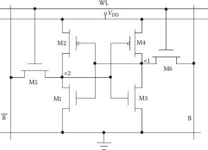
FIGURE 1.1
Six-transistor CMOS SRAM cell.
The first step in the read operation is to make bit lines B and high and to select a word line (WL). Enabling of the word line connects outputs of the cross-coupled inverter nodes x1 and x2 to B and respectively; depending on the data 1 or 0 stored, one of the bit-line voltages is pulled low by a small amount. The differential signal on B and lines is detected, is amplified to full logic value, and is made available at the output.
Assume that a high is stored at x1 and that both bit lines have been precharged to VDD. As the WL has been selected, it enables both the access transistor M5 and M6 after the initial WL delay. Data values stored at x1 and x2 are transferred to the bit lines by leaving B at its precharged value and discharging through transistors M1–M5.
For a cell to be of small size, it is essential to keep the size of all transistors as close to minimum as possible, though it makes their on-resistance large. Combined with larger value of bit-line capacitance in large memories, on-resistance makes the rate of drop in one of the bit-line voltage very slow. However, as soon as the difference of potential between B and reaches a small but critical value, the sense amplifier is activated to accelerate the change in the bit-line voltage. If the sense amplifier is not used, it will take too long to reach its final value so as to correctly read the data.
In the meantime, there is a problem to be sorted out during this read process, as M1 and M5 form a potential divider section. To prevent a substantial current from flowing through the M3-M4 inverter, it is necessary to keep the resistance of transistor M5 larger than that of transistor M1.
The boundary constraints on the device size (resistance) are derived by solving current equations at the maximum allowable value of the potential difference between B and . It is observed that even in the worst case the only requirement is that transistor M5 has to be made weaker by increasing its length, thereby making the basic cell a bit larger. However, in practice, this is not needed as the second bit line B, which is precharged to VDD and now clamped to node x1 at VDD, makes the read operation safe.
With transistor M3-M4 being of minimum size and M5 and M6 slightly weaker for read constraints, node x2 has to be below nearly 0.4 V (assuming VDD as 2.5 V), and a high cannot be written as such. Writing high can be ensured only if node x1 can be pulled below the threshold value of transistor M1. Fortunately, this constraint is met easily when both the transistors M4 and M6 are minimum-size devices [1].
As the bit lines are precharged to VDD, the PMOS transistors of 6T SRAM cell are not involved in the pull-up process. The requirement through this path is only to maintain the state of the cell by compensating for the small leakage currents, which is on the order of 10–15 A/cell [2]. This job can be done in different ways, and one such method is to use very large value resistors in place of the PMOS transistors M2 and M4 of Figure 1.1. Use of high-value resistors minimizes the static power consumption in addition to reducing the SRAM cell size by nearly one-third. Such large-value resistors in the teraohm range are fabricated in a compact form by using undoped polysilicon through a specialized fabrication process, reducing area and power consumption. However, the majority of SRAM designs use the conventional six-transistor configuration, because of constraints in applying special fabrication techniques for the resistors.
1.3 Dynamic Random Access Memories: Basics
A conventional SRAM cell used six transistors and a number of connect lines for storing one bit of information. The cell consumed large chip area, hence, raising cost per bit. As the two load transistors (M3 and M4 in Figure 1.1) were used only to provide a path for supplying leaked charge, they could be eliminated, resulting in a four-transistor memory cell as shown in Figure 1.2(a). Its operation was similar to the 6-T SRAM; however, it is required to be refreshed periodically, that is, the charge that was stored at the parasitic and gate capacitance of a node connected with high voltage bit line is required to be replenished.
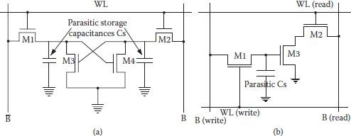
FIGURE 1.2
(a) Four-transistor DRAM cell with two storage nodes. (b) Three-transistor DRAM cell with two lines and two word lines. (Modified from CMOS Digital Integrated Circuits—Analysis and Design, S. M. Kang and Y. Leblebici, Tata McGraw Hill, 2003.)
To further reduce the complexity and size of the cell, the three-transistor DRAM cell was evolved from the four-transistor cell in the early 1970s, by eliminating one of the storage transistors, M4. As shown in Figure 1.2(b), transistor M3 remains the single storage device and it turns on or off depending on the presence or absence of the charge stored at its gate capacitances. One transistor each is used for the read and write access; M1 for read and M2 for write. The read operation of the three-transistor DRAM cell is nondestructive, but it still requires four connecting lines, two each for bit lines and word lines along with their contacts and vias.
1.3.1 Three-Transistor DRAM Cell
Elimination of the load transistors/resistors in a six-transistor SRAM cell and one driver transistor led to the three-transistor cell, which became the first popular dynamic memory cell as the stored data depended on charge stored at a capacitor located at a high-impedance node. A commercial dynamic RAM (DRAM) chip of 1 Kbit density was produced by Intel in 1970 using the 3T cell. It was then followed by 4 Kbit DRAM in a single-polysilicon, single-metal in 10 μm technology. Initially non-multiplexed addressing was used; however, soon address-multiplexed DRAMs were made available. At that stage sense amplifiers were simply made up of two static inverters and two switches with a bootstrapped output stage for fast charging of load capacitances.
1.3.1.1 Construction and Operation
A circuit diagram of a typical three-transistor dynamic RAM cell and some peripherals is shown in Figure 1.3. The transistors M1, M2, and M3 are made small to minimize the cell area. The data is stored on parasitic capacitance C1 in the form of presence/absence of charge on it. The storage transistor M2 is turned on or off depending on the amount of charge stored in C1 and transistors M1 and M3 act as access transistors for data write and read operations. There are two separate word lines for write and read. Separate data lines for read and write are also necessary as the stored charge of C1 would be lost if M1 was turned on during read. Necessary peripherals include two precharge transistors MP and MP′ and the column read/write circuitry.
The three-transistor DRAM cell and its peripheral circuitry operation are based on the two-phase nonoverlapping clock (CLK) scheme. The first half of each read and write cycle is a precharge phase (CLK being high) in which columns data input (write), DW, and data output (read), DR, are charged to valid high level through MP and MP′. As precharge is initiated with CLK going high, the column pull-up transistors became activated and the column capacitances CB and C′B are charged up to logic-high level.
All read and write operations are performed during the second phase, that is, when CLK is low. For the write high operation, is made low, turning the data write transistor Mw off, leaving the voltage level at line DW high after the precharge phase. Once the signal WLW is turned high during the second phase of (), the write access transistor M1 is turned on and the charge on CB is shared with C1 as shown in Figure 1.4(a). However, CB being very large in comparison to C1, charge transferred from CB is very small and voltage level of the column capacitance CB as well as that of storage capacitance is almost the same at logic-high level. When a high has been written, transistor M1 is turned off. Now transistor M2 remains turned on due to the storage capacitance C1 charged to a logic high.
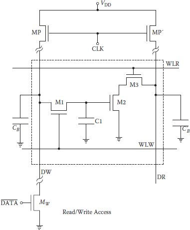
FIGURE 1.3
Three-transistor DRAM cell with the pull-up transistors. (Modified from CMOS Digital Integrated Circuits—Analysis and Design, S. M. Kang and Y. Leblebici, Tata McGraw Hill, 2003.)
To read a stored high, the read-select WLR is pulled high (once again with phase () low, following a precharge phase) which turns access read transistor M3 on, and conducting M2 and M3 create a conducting path between the column capacitance C′B and ground. The capacitance C′B discharges to ground and lowering of DR column voltage is detected by data read circuitry as stored logic 1 as shown in Figure 1.4(b). It is important to note that the read process is not destructive and the read operation can be performed repeatedly.
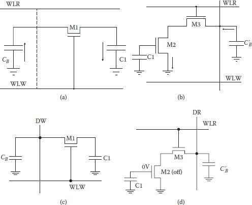
FIGURE 1.4
(a) Charge sharing while writing “1”. (b) The column capacitance C′B is discharged during the read “1” operation. (c) Both C1 and CB are discharged via M1 during the write “0”. (d) The bit line capacitance CB’ cannot discharge during the read “0” cycle. (Modified from CMOS Digital Integrated Circuits—Analysis and Design, S. M. Kang and Y. Leblebici, Tata McGraw Hill, 2003.)
For the write low operation, is made high, turning the write transistor Mw on, which pulls down the logic level of line DW low after the precharge phase (CLK). The signal WLW is turned high, during the second phase (); hence access transistor M1 is turned on. The voltage level on CB, which is at logic low, pulls the voltage level of C1 to low through M1, as shown in Figure 1.4(c). At the end of write low, the storage capacitance C1 is left with only a small charge, resulting in low gate voltage for M2, turning the transistor off.
To read the stored low, read select WLR is pulled high with (). The read access transistor M3 turns on; however, C′B cannot discharge because transistor M2 is off and no conducting path is available between DR line and the ground as shown in Figure 1.4(d). High level is retained on the DR column, which is interpreted by the data read circuitry as a low bit.
It is to be noted that repeated read operations can be performed because the read operation is nondestructive. However, charge stored on the storage capacitor C1 cannot be retained for long for various reasons of leakage, the main culprit being the drain junction leakage current of the write access transistor M1. Hence the leakage charge has to be restored at regular intervals. This restoration of charge or data, commonly known as refreshing the data, has to be done every 2 to 4 ms. For refreshing the data, it must be read, inverted, and then written back in the cell. Inversion of the read data is necessary during refreshing since the data output level reflects the inverse of the stored data. A number of refresh methods are used, the most common being one in which all the cells in a row are refreshed simultaneously.
An extra inverter is used in either the read or the write data path to get same logic in the memory data input and output. Simply put, refreshing does require some overheads; even then, cost per bit of DRAM is much less than for SRAMs. A major advantage of 3T DRAM cells is the absence of any static power dissipation during data storage, because of the fact that there is no continuous current path between VDD and ground. In addition, dynamic power dissipation is also reduced due to the use of precharge cycles instead of static pull-up. If static pull-up devices are used at the data output line DR, a higher average drain current would be needed after reading a high. Similarly, if static drivers are used at the data input line DW, fast changes in logic levels would require excessive power [3].
Dramatic reduction in cell size and complexity was achieved in a one-transistor DRAM cell, though at the expense of certain cell properties. One of the important constructional differences from 3T cell is shown in the one-transistor DRAM cell of Figure 1.5, which has an explicit storage capacitor Cs. Instead of using the parasitic gate and diffusion capacitances of the transistor M1 for data storage, a separate capacitor Cs must be fabricated. In the write operation, after the word line is enabled, the data is written into the cell through the transistor M1 and stored at the storage capacitor Cs. In the read operation, charge stored on the storage capacitor is shared with the bit line capacitance and hence the charge is changed significantly, making the read process destructive. For large memories, bit-line capacitance (column capacitance CB) is much larger than the storage capacitor; hence, only a small voltage change takes place at the bit line. It is therefore a must to detect this small change in voltage, amplify it quickly to full logic level, and rewrite (refresh) the data into the cell.
With only one transistor, one capacitor, and one line each for bit and word line, the DRAM cell consumes the smallest silicon area of all the static and dynamic memory cells. However, a minimum size storage capacitance is essential to develop small but sufficient voltage difference (Δv) on the bit line, which is to be detectable for correct read operation. The amount of Δv depends on the operating voltage (with a decreasing trend) and the ratio of the total bit line capacitance (which is increasing with increase in the size of the DRAM density) to the storage cell capacitance. DRAM designers and manufacturers have to make a continuous effort to develop and realize an effective minimum value storage capacitor that consumes as little chip area as possible.
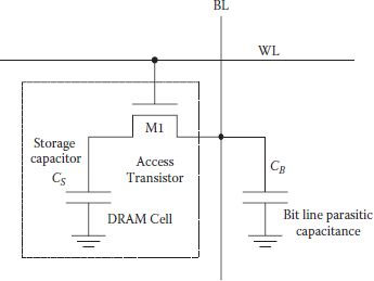
FIGURE 1.5
A one-transistor DRAM cell with its access transistor and data line. (Modified from CMOS Digital Integrated Circuits—Analysis and Design, S. M. Kang and Y. Leblebici, Tata McGraw Hill, 2003.)
Major reduction in cell area and complexity in comparison to a 3T DRAM cell was achieved in a single-transistor (1T) DRAM cell of Figure 1.5, which forced considerable difference in their operation. It happens because read-select and write-select lines are merged in single word line (WL) and data input and data output lines are also merged in single bit line (BL). Its basic operations are very simple. For both read and write, transistor M1 is turned on with the single WL. During the write cycle, data is written into the cell by placing data on the bit or column line. Depending on the data value, storage cell capacitance Cs is ether charged or discharged. However, before starting to read, BL is precharged to a voltage VPRE. Once WL is selected (high), charge distribution takes place between the BL capacitance CB and the storage capacitance Cs through the transistor M1. As a result, a small change takes place on the BL voltage of magnitude (Δν) as mentioned before, depending on the capacitance values (charge transfer ratio) CB and Cs, VPRE, and data voltage to be written. The direction of Δv depends on the logic state stored in the cell. The small voltage charge has to be converted to its final logic value, high or low, for completing the functionality of the (1T) DRAM cell. Thus, presence of a sense amplifier is a must for each bit line, not only for speeding up the read operation, as in the case of SRAM or 3T DRAM, but also for completing its function. Moreover, the sense amplifier design now becomes complicated due to the single-ended nature of 1T DRAM cell in comparison to the other cases where both data and its complement are available on two bit lines.
During the read operation the amount of charge on Cs is modified and remains so. Therefore, after reading, its original value must be restored or refreshed, so output of the sense amplifier is fed again onto the BL during the read process. Transistor M1 should remain on by keeping the WL raised during the refresh.
Another important point is the requirement of an explicitly fabricated capacitor Cs instead of using the parasitic gate and diffusion capacitance of the transistor M1. For reliable operation of the cell, the charge transfer ratio cannot be very small; hence, Cs must have a value not less than (say) 30 fF to have sufficient charge on it. Though small in absolute terms, realization of Cs in the submicron range is a tough problem. Some of the methods for realizing Cs, especially without consuming a bigger area, shall be discussed later in detail in Chapter 5.
1.4.1 One-Transistor DRAM Structures and Switching Waveforms—Review
In the early stages of the one-transistor DRAM cell, electrodes of the transistor and the storage capacitance were fabricated separately in a single polystructure [4]. With the introduction of double polysilicon structure, polysilicon electrode of the transistor and the polysilicon electrode of the capacitance were formed in different layers in an overlapping form, thus reducing the cell area. Further reduction in the cell area was achieved when triple polysilicon structures were developed. In this scheme bit line was fabricated as third polysilicon layers over the capacitor electrode. Reduction in the planar DRAM cell size resulted in considerable increase in the DRAM density. However, this arrangement in planar cell proved to be inadequate beyond 1–4 Mbit DRAM density. Several innovations and structures were developed for obtaining 30–40 fF storage capacitors without any increase in the cell area.
At initial stages, selection of a cell was done by the application of (N/2) address inputs each to both the row and column decoders in a (2N) capacity DRAM. For reading the data at the selected cell location, the chip is put in the read mode by asserting and enabling the chip through lowering the chip enable () pin of Figure 1.6(a). Figure 1.6(b) shows the timing relation between non-multiplexed address inputs and data available at the output pin Dout. Important timing specification for the DRAM are Read Cycle Time (tRC) and Read Access Time (tRAC), where tRC represents the minimum time required between any two read operations and tRAC is the duration between time instants when address is applied and the valid data becomes available at the output.

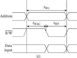
FIGURE 1.6
(a) Typical functional diagram of a 1kbit DRAM. (b) Typical DRAM Read cycle. (c) Typical DRAM Write cycle. (Modified from CMOS Digital Integrated Circuits—Analysis and Design, S. M. Kang and Y. Leblebici, Tata McGraw Hill, 2003.)
For writing data to a DRAM location, is made low with valid data available at the data input pin Din. As shown in Figure 1.6(c), Write Cycle Time (tWC) is the minimum time required between any two write operations and it normally equals tRC, and the Write Access Time tWAC is the duration between time instants when is made low or address is applied and when valid data is written. In addition, Write Pulse Width tWP is the duration for which input must remain present and then can change to high for another read/write.
For refreshing the DRAM, all the cells are accessed periodically through selecting every row one by one using the falling edge of the strobe. All the cells in a row are read and written back.
1.5 Initial-Stage DRAM Technology Developments
In spite of increased complexity especially due to refreshing, low cost per bit of DRAM has made it the memory of choice for large-volume commercial applications. Both 3T and 1T DRAM configurations became standard for various positive reasons. Even in 1973, one-transistor DRAM was easily available for 4 Kbit density. However, as DRAM’s read operation is destructive, sufficient value cell capacitance Cs was essential to get adequate value of voltage differential on bit line, especially as its capacitance increases for large-density memories. A number of technologies contributed in the progress of the DRAM developments—for example, use of high-permittivity dielectric material and advanced structures for the storage capacitance, without increasing effective occupied chip area; which was crucial and shall be studied separately in Chapters 3 and 5. Other key factors included advanced processing techniques including (but not limited to) photolithographic and etching techniques, without which it was not possible to continuously reduce DRAM size per bit. Improvement in array architecture like folded data line arrangement for noise reduction [5] and ½VDD data-line precharge [6] were also extremely important factors.
Advantages of precharging to ½VDD are manifold; for example, it improves noise immunity, reduces power consumption of bit line, and reduces electric field intensity across the capacitor Cs. Bit and sensing line equalizers are used to precharge the bit lines and sensing nodes to the precharge level of ½VDD before any operation starts. Considerable improvement in supporting circuit technologies like improvements in bit line signal sensing, use of dynamic amplifiers and drivers, and changeover to CMOS circuit, and so on, were other very important developments. Address transition detection (ATD) circuits were found to be quite useful in saving access time by performing useful circuit functions for those durations which were earlier wasted because of RC delay in word lines. Some of the technical developments shall be discussed in this chapter and others shall be taken at later stages in Chapters 3, 4, 5, and 6.
A DRAM cell uses a single bit line through which data is written into as well as read from the charge storage capacitor. When storage capacitor is connected to the bit line, charge transfer takes place between the storage capacitor Cs and the bit line capacitance CB. An important figure of merit is the charge transfer ratio, given as Cs/(Cs + CB). Value of Cs has to be kept small so that it occupies less chip area where as CB goes on increasing with the increase in the size of DRAM. Thus an amplifier commonly known as sense amplifier must be available, for the reason already mentioned. The sense amplifiers used with DRAMs are generally different from sense amplifiers used with SRAMs and ROMs. DRAM sense amplifiers are discussed in more detail in Chapter 8.
In SRAM sense signal is available differentially on the two bit lines, where as DRAM is essentially a single bit line structure. Arrangement has to be made of a reference bit line against which differential voltage change is detected. Since storage capacitance charge is disturbed in the reading process and it also loses charge due to leakage, its original state cannot be restored/refreshed unless done intentionally through the sense amplifier. Once sense signal is amplified to its full logic value, it remains stored in the sense amplifier output until the cell is precharged for the new read operation. Since one sense amplifier is connected with one row, it effectively acts as and is referred to as row buffer also. Correct detection of small column signal or bit line charge is one of the most difficult parts of the sense amplifier design for 1T DRAM cell.
A read and refresh schematic for a 1T DRAM is shown in Figure 1.7 in a simplified form. In normal course, small voltage change in single bit is difficult to detect, so the bit lines are divided in two halves. Consequently bit-line capacitance is also reduced by half, doubling the charge transfer ratio. The regenerative switching of dynamic flip-flop, working as a sense amplifier, detects the small deviation in bit line signal and restores/refreshes the high or low signal level [7].
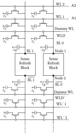
FIGURE 1.7
Sense/refresh arrangement with dummy and storage cells. (“Storage Array and Sense/Refresh Circuit for Single Transistor Memory Cell,” K.U. Stein, A. Sihling and E. Doering, IEEE Int. S.S. Circuits Conf., pp. 56–57, 1972.)
To read from 1T DRAM array, column lines (bit lines) are precharged to VPRE. Dummy cells on both sides of the sense amplifier are also turned on, charging the dummy cell capacitor to VPRE. One of the word lines, say WL1 is made high so that first set of cells on the top side is selected. Simultaneously, the dummy cell, WLD′ located on the opposite side of the sense amplifier is selected. No change of voltage takes place on the bit line BL0 as its voltage level is same as that of the voltage of WLD′. However, the voltage level on the top side of BL0 will change in value toward higher or lower side of VPRE depending on whether a high or a low is stored in the cell. It is important to select dummy cell on the other side of the sense amplifier with respect to the selected cell to balance the common-mode noise. The direction of the resulting small differential voltage difference between the selected cell and the dummy cell on the opposite half determines the final data state to be sent to the output buffer.
1.5.2 Open and Folded Bit-Line Structures
While differential sensing is the preferred approach, some variants, like charge-redistribution amplifiers schemes, were used in DRAMs, because of their inherent single-ended nature. However, this scheme works with a very small noise margin and needs a very careful design. At the same time with increase in DRAM density, noise components start increasing and single ended sensing does not remain a practical solution. Circuit modifications are done so that a differential sensing becomes possible, like that shown in Figure 1.7 where a differential amplifier is placed in the middle of the bit line. This scheme of having the bit line is called open bit-line architecture (OBLA). Advantage of the OBLA is that every crossing point of word line and bit line contains a storage cell. One of the important advantages of the OBLA is that one transistor–one capacitor DRAM cell and its interconnections with WL and BL can be fabricated in 4 F2 chip area, where F is the minimum feature size during the fabrication process, independent of the working technology. With continued demand on reducing the cell size, F become further small, bringing word lines and bit lines closer, storage cell smaller; and size of the transistors used in the cell as well as in the sense amplifiers also has to go down. However, it has limitations in terms of noise minimization. Coupling noise between word line and bit line increases considerably especially when word line is selected and the bit line is low. Parameters of the transistors in sense amplifiers like threshold voltage become mismatched and produce noise; two halves of the OBLA also do not match exactly. All these and some other noise sources combine together to make this architecture less robust. Many corrective measures have been suggested to reduce noise components; however, changeover to folded bit-line architecture (FBLA), as shown in Figure 1.8, is extremely useful in reducing the differential noises [8]. In this arrangement sense amplifiers are at one end, instead of being in the middle, and column decoders are at the other end. As the bit line is folded back on itself, noise generated on the column decoders appears as common mode and gets canceled. As seen from the diagram, cells are not placed at every cross section of word line and bit line. Minimum possible cell area in this architecture is 8 F2.
DRAM operating modes can be classified as (1) asynchronous and (2) synchronous. In asynchronous mode all control and operational signals depend on and strobes whereas in synchronous mode, these depend on a system clock.
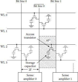
FIGURE 1.8
Memory architecture for a typical DRAM with folded bit-lines.
First is made low for any DRAM operation, which, along with activating , starts operation with row address buffers, row decoders, word line drivers, bit-line sense amplifiers, and so on. Depending on the address supplied by the selected combination of row and column address in a multiplexed address scheme, bit location is selected on the falling edge of and , respectively. Some precharge time is needed by the and strobes before locating a new address. Time duration between two falling edges is called read/write cycle time as mentioned in Section 1.4.1. Figure 1.9(a) shows simple single-bit access asynchronous operation mode. Typical operating frequency in this mode is in 20–30 MHz range. Other modes of asynchronous DRAM operation are page mode, nibble mode, static column mode, fast page mode (FPM), and extended data out (EDO).
Figure 1.9(b) shows the timing diagram of a page mode read and writes. With going low, selected word line is made high. Prior to the row selection it is precharged to a voltage VPRE (usually VCC/2) and the input/output (I/O) pin is in the high-z state. Next is made low and column address is decoded which selects addressed bit line, and data on the select bit location is read and goes out through (I/O) pin. When goes high, I/O pin goes back again to the high-z state. Another bit line can be accessed through the column address decoder, from the same selected word line to either read or write. The entire bit in a selected word line can be accessed by raising all bit lines one-by-one and total bits in a word line form one page. In fact, for bigger-size memories when the cell array is horizontally divided in N blocks, generally one word line address opens one word line in each of the block; in that case size of the page is increased by a multiplicative factor N.
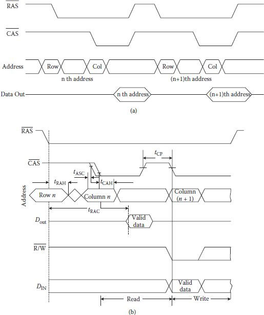
FIGURE 1.9
(a) Single bit read in an asynchronous DRAM. (b) Page mode operation.
In the fast page mode (FPM), column address is applied early, that is, even when is high. Some of the time taken in propagating the column address and high overlaps, this makes the mode of operation fast. Extended data output (EDO) is simply an FPM scheme in which the output is not forced to go to high-z state when goes high. In the nibble mode operation, column address changes by strobing through an internal presettable counter. Column address is loaded into the counter when the goes low first time (after the first RAS changing to low). With toggling, next cells are automatically selected for reading or writing without providing column address. In the nibble mode only four cells are selected in this way—hence the name nibble mode.
In the static column mode operation flow-through latches are used in the column address path. With low, when the column address is changed, it directly goes to the column address decoder; it does not wait for the falling edge of the . Output of the DRAM does not go to the high-z state and DRAM speed is increased. From the above discussion it is obvious that DRAM is being made fast by keeping a row selected, thus saving time.
Figure 1.10 shows a simplified structure of a 64 Mbit FPM DRAM with number of rows, columns, signal lines, and so on, also mentioned alongside [9]. Captions inside the blocks in the figure state their use. DRAMs based on other modes of operation have similar structures with subtle variations. All DRAM structures contain a logic circuitry in addition to the function blocks, like decoders, data buffers, sense amplifier array, and core array. The logic circuitry controls and assigns direction to all signals inside the DRAM chip, and in addition, it sends and accepts the signals from outside. In Figure 1.10, control logic receives, , , and signals as shown, as well as data-in at the I/O module. The rest of the signals inside the chip are generated and directed by the control logic. Important to note is that all movement of data is asynchronous in nature as it is not controlled by an external clock. The asynchronous nature of DRAM working has the advantage that different memory controllers can be designed at different frequencies depending on the internal clock generators. However, asynchronous nature restricts the use of pipelining, which is an important tool for speeding up processes in digital systems.
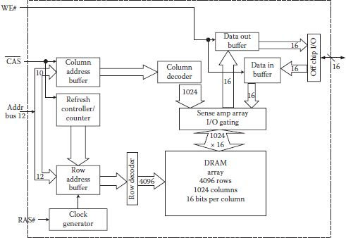
FIGURE 1.10
A 64 Mbit fast page mode DRAM simplified architecture.
Up to 16 Mbit density level, basic structure of Figure 1.10 was used, though other improvements were done for performance enhancements. However, the structure had major limitation in terms of only small improvement in DRAM’s access time. In 1993, JEDEC standards committee decided a new standard for synchronous operation of DRAMs in which all signals were to operate on a single clock. All control logic on the DRAM chip was to depend on this external clock. This brought a remarkable change in the DRAM complexity and the way bits moved around, and possibility of further increasing DRAM speed became a reality. A synchronous interface is added to the basic DRAM core so that all commands and operations are dependent on the rising edge of the master clock. Figure 1.11 shows a block diagram of a DDR synchronous DRAM (SDRAM) comprising of basic DRAM array with 32 bit I/O, command interface on the left and a DDR SDRAM interface on the right [10]. All previous generation signals like , , , and continued to do the same operation. Fundamental operations remained as before; however, because of modified structure of DRAM having multiple banks, necessary changes were to occur in the selection of row, column, and particular bit(s). Usage of number of banks enhances the speed of the DRAM, partly because of reduced bit line length for any selected bit(s), but a major contribution toward speed enhancement is because of the usage of pipelining. While one bank may be in precharging state, reading may be taking place in other bank and so on. latency and burst length and burst type are stored in a mode register; and stored latency field value decides the number of cycles between output and assertion of column read command. Burst type value determines the ordering of the data availability and the length gives the number of columns that the SDRAM will return to the memory controller as a result of one column read command. The mode registers go on becoming more complex for advanced synchronous DRAMs, commonly known as DDRx SDRAMs.
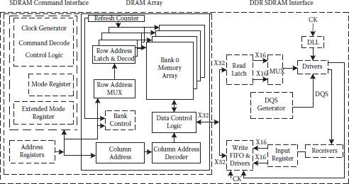
FIGURE 1.11
Block diagram of a DDR SDRAM showing the underlying SDRAM and DRAM. (“Application Specific DRAMs Today,” B. Prince, Proc. Int. Workshop on Memory Technology, Design and Testing (MTDT), 2003.)
DRAMs, which have been used as main memory devices, have quadrupled in size with every generation, but with limited speed improvements. Asynchronous DRAMs, be that EDO or Burst EDO, have not exceeded the bus speed beyond 66 MHz. The asynchronous interface and internal logic cannot achieve the page mode accesses required for bursts at over 66 MHz. High speed SRAM caches usually filled the bandwidth (= bus width × cycle frequency) gap between CPU and DRAMs which heavily relied on low miss rate to avoid main memory access. However, SRAM cache could not satisfy the requirements of software applications like multimedia, so miss rate increased. Hence improvement in bandwidth was possible with increase in bus transfer rate. In an intuitive evolution from the single data rate SDRAM, data transfer was doubled in double data rate (DDR) SDRAM. The data was transferred on both the rising and falling edges of the clock, though all commands and operations took place only on the rising edge of the clock [11].
In DDR SDRAM, a wide internal bus prefetches two words simultaneously, and they are parted as two separate words of equal width. Prefetch doubles the data rate with an additional advantage of lowering the array power as the array runs at half speed, compared to an array with higher data rate without prefetch. As an example, 32 bits are fetched from the array and converted into two 16-bit words as shown in the right-hand side of Figure 1.11, the DDR SDRAM interface. Choi and others [12] gave a 16 Mbit SDRAM using pipelined 2-bit prefetch architecture. A delay locked loop (DLL) shown in the SDRAM interface part of Figure 1.11, is used to lock the edges of the output and data strobe to the system clock.
In 1993, Takai and others presented a 3.3 V, 512 k × 18 × 2 bank synchronous DRAM using a 125 MHz clock with three stage pipelined architecture [13]. Use of the pipelining of the information, in and out of the SDRAM having synchronous interface, enhances the clock speed considerably. Speed is also increased using multiple banks, which are shown in the middle part of Figure 1.11. Even multiple banks can also be left open using the loaded sense amplifiers as caches.
The commodity DDR SDRAM is 256 Mb, with four array banks, 266 MHz data rate having 2.5 V stub series terminated logic 2 (SSTL2) interface. A terminated 2.5 V SSTL2 interface with low swing reduces ground bounce, hence improving system speed.
The DDR2 SDRAM simplifies the DDR SDRAM operation. Elpida Corporation gave a DDR2 SDRAM in 2002 having 256 Mbit densities, operating at 1.8 V and contained four array banks [14]. It used a clock speed of 200 MHz and provided data rate of 400 Mb/sec/pin in a large system using DIMMs and a data-rate of 600-Mb/sec/pin in a point-to-point system. A four word prefetch with two way data interleave was used to improve speed. In 2004, Fujisawa and others [15] gave a 1.8 V, 400 MHz clock, 800 Mbps/pin, 1 Gbit DDR2 SDRAM. It used a drivability-adjustable off-chip driver for DDR1 operation and an adjustable on-die termination register in DDR2 operation. A dual clock input latch scheme helped in reducing the cycle time from 3.0 ns to 2.15 ns. Several performing schemes were given in subsequent years for DDR2 and then for DDR3. One of the given configurations, SDRAM was a 1.5 V, 1.6 G bps/pin 1 Gbit DDR3 SDRAM, which used an 80 nm triple-metal dual-gate poly CMOS process [17].
Variants of DDR SDRAM have been reported in large numbers. Since the scope of discussion here is limited, the topic is not treated in depth. As mentioned before, specific applications required further higher bandwidths and graphic memories has been one such area. To achieve required bandwidth novel I/O technologies have been adopted and a whole new area of advanced research has been opened. Graphic DDR4 SDRAM at 4 Gb/s pin speed and GDDRS SDRAM at 7 Gb/s pin bandwidth have been realized [18] and further improvements are ongoing.
1.7 Silicon-on-Insulator Technology
With other fabrication processes being almost the same as in the bulk complementary MOS (CMOS) process, fabrication in silicon-on-insulator (SOI) technology is performed in a thin layer of silicon, which is deposited on a thick layer of SiO2. A number of techniques are available for producing starting wafer which is the basic difference with the bulk CMOS. SIMOX (separation by implanted oxygen) is the most commonly used technique in which a high dose of oxygen (O–) ions prepares a silicon wafer with a high quality layer of SiO2. Energy level of the implant is so selected that the peak of the implant is nearly 0.3–0.5 μm deep in the silicon. Crystallinity of the silicon surface is restored by heating it at 400°C during implantation, and then post-implant annealing is performed. Crystalline silicon surface layer is usually 100–300 μm thick [18] and if necessary epitaxial silicon is grown to increase its thickness.
Along with the use of lateral isolation techniques, completely latch up-free circuits are realizable in the SOI technology. Reduced parasitic and better on-off characteristic of transistors are its basic advantages. Other advantages include reduced short channel effect (SCE), reduced hot electron generation and sharper sub threshold slope. Usage of SOI chips remained restricted in high-performance, high-cost applications for long because of economic reasons. However, with continued reduction in minimum feature size in the bulk silicon technology, cost differential has come down considerably along with its improved performance in terms of reduced parasitic capacitance, lower threshold voltage, and body charging effects. Due to its floating substrate, kink effect, a dip in current-voltage relation, is observed in SOI MOSFETs, but it has been virtually eliminated in fully depleted SOI MOSFETs.
In another method wafers are produced in so-called bonded SOI wafer production in which ion implantation is not used. First two silicon wafers are heated so that oxide is formed on their surface. Next, the two oxide surfaces are bonded together to form the buried oxide, and one side of the silicon is partially removed. The SOI wafer is annealed and polished finally.
Figure 1.12 shows the cross-section of a partially depleted (PD) SOI device, in which every fabrication is the same as that in bulk CMOS except that buried oxide was already present. Silicon body having thickness tsi is completely surrounded on three sides and partially opens at the top. For a PDSOI device depletion region extends into the body of FET, as shown in the figure and does not deplete all the charge in the body. Remaining charge in the body is mobile and variable as it depends on the terminal voltages. This mobility of charge makes PDSOI device unique and is responsible for quite different characteristics than a bulk MOSFET.
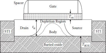
FIGURE 1.12
Cross-section of a partially depleted SOI FET. (Modified from SOI Circuit Design Concepts, K. Bernstein and N. J. Rohrer, Springer Science, 2007.)
In PDSOI-based MOSFETs, current-voltage characteristics are not constant as they depend on the amount of charge in the body. This prominent property is known as the history effect. Total charge in the body is the algebraic sum of incoming and outgoing charges due to various reasons like impact ionization which generates electron-hole pairs, junction leakage, source-body n-p junction, and so on. All of these depend on the gate, drain, and source potential.
Impact ionization is an important contribution of charge to the body, and it is observed that its peak occurs when the gate voltage is half of the supply voltage. So, any operation in which gate voltage remains close to VDD/2 for long duration, increases the body potential and threshold voltage variability. There are many more attributes and characteristics different from bulk CMOS and texts like [19] can give an excellent exposure.
DRAMs on thick SOI substrate were fabricated as early as 1994 at 256 Mbit density levels [20] and soon SOI DRAMs for multi-gigabit density were proposed [21]. For increased density on SOI substrate one transistor-one capacitor DRAM quite a few schemes were given, however a capacitor-less single transistor DRAM on SOI substrate was given in 2001 [22]. The idea of not using a capacitor was with the purpose of saving chip area and the complex fabrication steps involved in three-dimensional capacitors. Few such capacitor-less DRAMs are briefly discussed in the following section.
It was expected in 2007 that by 2011 high-end processors would be using 83% of chip area for the memory [23]. Hence, the designer shall be forced to accommodate continuously increasing amount of memory in as small chip area as possible. Though 1T1C DRAMs are continuously increasing density through many technological improvements, circuit innovations, and advanced transistors and capacitors, use of external capacitor was completely avoided in a slightly different idea in capacitor-less DRAMs. While pursuing the idea it was important not to add new complexities and materials in the already existing procedures, especially at sub-100 nm technology level. The first such attempt was made in 2001 [22] and in the following years [24] in which capacitor-less 1T DRAM was proposed using SOI substrate. Floating body of a partially depleted (PD) SOI MOSFET was used as a charge storage node, which served/replaced the purpose of the physical capacitor of a conventional 1T1C DRAM.

FIGURE 1.13
Changeover to capacitor-less DRAM. Presence or absence of excess positive charge decides its state. (Redrawn from “Masters of Memory,” S.K. Moore, IEEE Spectrum, pp. 45–49, 2007.)
A capacitor-less SOI DRAM cell have been given much earlier, using two transistors, but it was operationally complex and occupied larger chip area [24], whereas the aim was to get a DRAM cell in an area of 4F2. Such a simple structure, which used three signal lines and a single channel, was given [23] which used the property of body-charging effect in PD SOI MOSFET, an effect considered problematic in normal SOI MOSFET working. Utility of the concept was shown on MOSFETs at 0.25 μm and 0.13 μm SOI CMOS technology. Positive substrate charge was created through impact ionization near the drain by applying a positive drain voltage pulse, which increased the source current and it corresponded to a high. A high can also be written using source side impact ionization by negatively biasing the drain and gate. For a 0.25 μm NMOS, writing operation took 3 ns. A low state was written, again in 3 ns, through removing holes from the substrate at the source or drain side. Figure 1.13 shows the basic storage of high and low. Data stored was read by comparing the source current with that of a reference cell using a current sense amplifier. Reading was done at a low drain voltage to make it nondestructive.
At reduced feature size, cell retention time becomes extremely important. Moreover, sense margin obtained in early stage of capacitor-less SOI based DRAM was low. A double-gate fully depleted FinFET DRAM at gate length less than 50 nm [25] was used to try to overcome the limitation.
Excess holes can be generated not only by the impact ionization but also by gate-induced drain leakage (GIDL); due to band-to-band tunneling, GIDL current can flow under both negative gate bias and positive drain bias. One-transistor DRAM using GIDL is able to operate at high speed and with lower power consumption. Double-gate depleted FinFET DRAM was used to overcome limitations caused by the reduction of minimum feature size. The front part of such a FinFET functioned as a conventional transistor, whereas the back gate MOS structure was used to store excess holes in the body with proper biasing condition. Since the double-gate Fin DRAM uses very low doping concentration in the floating body, junction leakage current is very low and hence retention time is improved.
Several capacitor-less DRAMs have been reported other than the one mentioned above, but some of these were either simulations [26,27] or using wafer bonding approach [28], or used SOI substrate [29]. With a distinct shift, a double-gate capacitor-less 1T DRAM was fabricated on a bulk-silicon wafer [30]. Obviously, it was an advantage in terms of ease in fabrication process and integration. Functionality is similar to the earlier case with one gate side working as conventional MOSFET and the other gate creates floating-body storage node. To retain the excess holes in the body for a memory action, the second gate is to be reverse-biased. Because of the vertical orientation of source and gate, the two gates are physically isolated and there is no lithographic constraint on the channel length. As before, use of low doping concentration, junction leakage is low resulting in higher retention time. Impact ionization generates holes at the drain side and a quasi-floating-body is created in a few nanoseconds at the back (second) gate interface. Scaling of such a DRAM was achievable even up to 22-nm technology node. Apart from being called capacitor-less DRAM [26,28,30,31] it has been given some other names like zero (ZRAM) [22], unified (URAM) RAM [32,33], or simply 1T DRAM [34]. In the URAMs, functions of DRAM and nonvolatile memory are combined. It is expected that more efforts shall be made to make this kind of memory more acceptable for manufacturing.
1.8 Advanced Nonvolatile Memories
A large number of semiconductor nonvolatile (NV) memories, such as ROMs in which data is written permanently, PROMs in which data is entered by the user only once, and floating-gate technology EPROMs and EEPROMs in which data can be written and erased with endurance cycle in the range of 104–106 have been widely used. Special NV memories, which use static RAM array and backup array of EEPROM as well as those based on DRAMs and MNOS [35], were also in development. Memories in which all contents or big blocks of data can be erased electrically called flash memories in NOR and NAND structures are giving hard competition to the DRAMs. Requirements from the NV memories are very similar to those of other semiconductor memories, like low cost per bit, high scalability, fast access and read/write operation, and low power consumption. In addition its endurance cycle should be as high as possible. None of the NV RAMs has all the qualities and continuous efforts strive to find better NV technologies.
One such successful attempt was in the development of thin film ferroelectric technology in which lead zirconium titanate PbZr4Ti1-xO3 (PZT) (and few other dielectrics) was used as nonvolatile capacitive storage element to give ferroelectric random access memories (FRAMs) [36]. FRAMs were found to have higher endurance cycle and low cost per bit in comparison to other NV RAMs in the 1990s.
Another technological development is in the form of magnetoresistive (MR) memories (MRAMs), which are based on possible change in a material’s magnetoresistance in the presence of a magnetic field. The MR effect has been effectively utilized in forming storage elements comprised of a pair of magnetic film strips with a dielectric in between [37]. MRAMs have been fabricated in Mbit density. Spin-torque transfer (STT) magnetizing switching has further given a significant technological advancement, in which external magnetic field is not necessary that was required in a conventional MRAM. Read operation in MRAMs is non-destructive, and it possesses considerably higher endurance cycle in comparison to FRAMs.
A high-performance NV memory technology has been developed in the form of phase-change RAM (PCRAM), which uses GST (GeSbTe) chalcogenide alloys as memory elements [38]. The GST alloy is set to crystallize and reset or amorphize in a reversible process by the application of proper heating. Effect of the transition between set and reset is that resistance ratio between the two is in the range of 10 to 104, which is mainly responsible for giving large signal sensing margins. Theoretically PCRAMs have almost unlimited scalability. However a major limitation of PCRAMs is the requirement of larger current during reset process of GST, which in turn, requires large size of cell transistor. Efforts have continued to overcome the limitation.
Be it EPROM or EEPROM, memory is programmed using alteration in the threshold voltage of floating gate transistors. The programmed transistor retains modified threshold even when the supply is turned off. For reprogramming, an erase procedure was required, and it is this erase procedure which was mainly deciding the type of NV memory, its advantages, its limitations, and its applicability. By 1992 conventional EPROMs and EEPROMs lost their space to flash memories because of their larger cell size and the inconvenience in their use, especially for the erase procedure.
Flash memories have combined better properties of EPROM and EEPROM of higher density and faster programming capability, respectively. In flash devices content of the memory cells is erasable through the use of an electrical erase signal as a whole or in terms of big blocks. Most of the flash memories use avalanche hot-electron injection for programming of the cells, wherein a high-voltage application between source and gate-drain terminals converts electrons as hot with sufficient energy to cross thin gate oxide and get trapped on the floating gate, thus changing threshold voltage of the transistor. Erasure mechanism is through Fowler-Nordheim tunneling, as in the EEPROM cells.
A number of similar flash cells are available. One of these shown in Figure 1.14(a) is the ETOX flash cell given by Intel [39] which is similar to a FAMOS gate, except that tunneling gate oxide is very thin (~10 nm). Programming is performed through the right-hand area as shown, by applying 12 V on gate and drain with source grounded. Erasing is performed using left-hand area with gate grounded and the source at +12 V. Flash cells can be connected in NOR ROM or NAND ROM. For a NOR ROM, the programming cycle starts with complete erasure along with a monitoring procedure of the threshold voltage of all the transistors for reliability’s sake; writing is then performed for the selected cells. The memory is then ready for read operation(s) as shown in Figure 1.14(b). NOR ROM architecture has fast random access but writing the cell is slow on account of monitoring of the threshold voltage of the transistors. If faster random access is relaxed, cheaper, denser, and fast erasing and programming with fast access is obtained in NAND ROM where 8 to 16 floating-gate transistors are connected in series, as shown in Figure 1.14(c). Chain of the transistors is sandwiched by bit line and source line in series with two select transistors 1 and 2 [40]. Here select 1 ensures selectivity and select 2 ensures no current flow during programming of a cell. The cell can be erased as well as programmed using Fowler-Nordheim tunneling. Program cycle consists of (1) initial program by applying 20 V to the selected control gate (with 10 V applied to the rest of the gates) and grounding the bit lines for writing 1. For writing 0, bit lines are raised to 10 V. (2) For reading, control gate of the selected cell is grounded and 5 V is applied to the gate of the rest of the cells, with both select transistors 1 and 2 enabled.
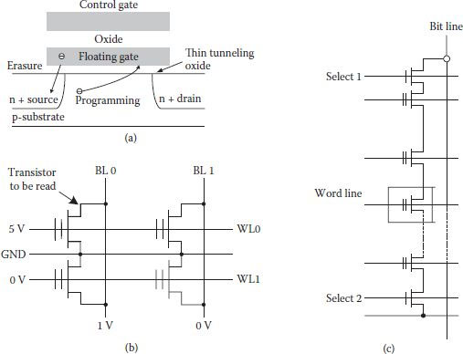
FIGURE 1.14
(a) ETOX device as used in flash EEPROM memories. (b) Basic read operation in a NOR flash memory. (c) NAND-based flash DRAM module. (Modified from Digital Integrated Circuits: A Design Perspective, J.M. Rabaey, A. Chandrakasan and B. Nikolic, Pearson, Prentice Hall, 2003.)
Many more architectures for flash memories are available, though the basic principle remains same. An excellent review is available in [41]. It is observable that all early flash memories used high voltages (>10 V) for programming and erasure. For those memories requiring smaller currents on chip charge pumps could be used. However, larger current memories needed external supply, increasing complexity of the system.
A unique advantage of flash memories is multibit storage in a single cell which enables high densities. However, there are limitations in scaling the technology node. Since NOR flash memories need higher drain voltage for hot electron generation and their injection into the floating gate, non-scalable Si-SiO2 energy barrier height becomes a basic scaling limiting factor [42,43]. This high drain voltage can create intercell interference. Furthermore, scaling down of transistor has short channel effect (SCE). To minimize these problems NOR flash technology adopted use of high dielectric material with low energy barrier height like HfO2 [44] and advanced transistor like FinFET [45]. It was expected that sub-50 nm technology node could be deployed for NOR flash. NAND flash structure has more scaling capability because of its architecture and device physics [46] but cell-to-cell interference is a major limitation for scaling. Closely placed cells have capacitive coupling which makes it probable to over program or under-erase failures [46]. As the NAND flash technology moves toward 50 nm sensing signal margin is reduced in conventional-type transistors. To overcome the scaling problem, once again use of low dielectric material and FinFET based SONOS (silicon-oxide-nitride-oxide-semiconductor) cell structures [47] are very effective.
Simplest cell structure and smallest cell size per bit make the NAND flash suitable for highest density. Packing density is further accelerated by 3-bit per cell and 64-bit cell string structures [48]. Kurata et al. [49] gave a 1 Gbit multilevel cell (MLC) flash memory with precise control of Vth. In 2007, Shibata et al. [50] presented 16 Gbit flash memory using 16-level cell at 70 nm technology. Another important flash cell development revival was in the form of a MONOS (metal-oxide-nitride-semiconductor) cell first given by Nozaki [51] in 1990 for embedded flash in microcontrollers, workable at 5 V. Depending on the speed of evolution of NAND DRAM, it was expected that 32–64 Gbit flash memories would be available by 2010 in sub-40 nm technology [52]. However, it required overcoming the scaling challenges in the form of lithography constraints and device characteristics. One of the promising techniques is the self-aligned double patterning [53], which has been shown to be feasible at 30 nm node. Main challenges in the device characteristics are coupling ratio, and previously mentioned cell-to-cell interference and SCE which becomes acute at smaller technology level. One of the solutions for reducing cell-to-cell interference comes in the form of charge trap NAND flash memory [54,55] and it also meets the coupling ratio requirement. Requirement of sufficient Ion/Ioff ratio in transistors beyond 40 nm is difficult to solve as it needs an increase in channel doping, which in turn increases depletion capacitance, degrading Vpass window; additionally, the problem of SCE is to be solved. Advanced transistors have been used for this purpose; a three dimensional transistor hemi-cylindrical FET (HCFET) appears to be a suitable candidate [56]. Beyond the 20 nm node, the most effective method of increasing NAND flash density is the vertical cell stacking [57,58]. It is expected that it will reduce the mentioned constraints of lithography, cell-to-cell interference, SCE, coupling ratio, and so on.
1.8.2 Ferroelectric RAM (FRAM)
A FRAM cell is similar to a DRAM cell, as it comprises an access transistor, a word line, a bit line, and a storage capacitor, which is realized using two metal electrodes and dielectric film in between. Similarity ends here as the dielectric used is a thin film of ferroelectric material. A number of such materials are available; however, lead zirconium titanate (PZT) is most commonly used, as it can store large charge on the order of 10 μC/cm2 (nearly 100 times that for SiO2). In a ferroelectric capacitor, when a positive voltage more than a critical voltage called coercive voltage is applied, the dielectric film is polarized in the positive direction and reaches a saturation level. If the applied voltage is removed, the film still remains positively polarized to a slightly lesser level than that of saturation level, and the level of polarization is called remnant polarization value. This polarization level is normally defined as low state. Changeover of applied voltage in the negative direction converts the polarization of the film in the opposite direction, reaches saturation, and once again rests at the opposite remnant value when applied voltage is removed. This value of polarization now corresponds to high state. The net result of the operation is that two digital states are clearly defined as the difference between remnant polarizations and the polarization condition remains in either state without application of external electric field or current. Hence storage of data does not require power for data retaining [59].
FRAM cell comprising one transistor and one capacitor operates similar to DRAM cell; however, the dual-element cell shown in Figure 1.15(a) is more common for reliability reasons as common-mode variations in the ferroelectric capacitor get canceled. In fact, one of the earliest FRAMs used such architecture to realize an experimental 512 Mbit NV memory. Here, a word line controls two access transistors, bit (BL) and bit bar () collect charge from the capacitor, and an additional component is a common drive line which actively drives the capacitors. Figure 1.15(b) show FRAM memory in its basic form [36]. For the write operation, desired data is supplied to the sense amplifier, which in turn sets BL and in such a way that when the drive line is pulsed high, grounded BL writes a low. When drive line returns to ground level, a high is written in the second capacitor connected to . Data written on the BL represent the stored data. During the read operation of FRAM, the sense amplifier is turned off with bit lines floating, and the drive line is pulsed. Because of opposite polarization in the differential cell BL and combination provides signal differential of the two.
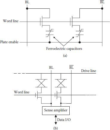
FIGURE 1.15
(a) A dual-element memory FRAM cell. (b) Read/write basic arrangement in FRAM. (Redrawn from Semiconductor Memories, Technology, Testing and Reliability, Ashok K. Sharma, IEEE Press, 1997.)
For the purpose of scaling of FRAM, it is observed that limiting factor is the realization of capacitor. Very obviously, sensing signal in FRAM depends on the capacitor area and the remnant polarization charge density mostly depending on the thin ferroelectric film. Beyond a certain FRAM density level, instead of planar ferroelectric capacitor, a three-dimensional structure has to be employed to increase its area, which may bring down the cell size in the range of 6 F2 to 8 F2. Thickness of the ferroelectric film is also reduced to get same remnant polarization at smaller cell size, but it also has a practical limit, possibly a few nanometers. At thin ferroelectric layer, its degradation reduced the remnant polarization and data retention time, which is greatly improved by better film growth techniques like MOCVD and optimization of seed layer.
1.8.3 Magnetoresistive RAM (MRAM)
Magnetoresistive random access memory (MRAM) is based on the integration of magnetic memory elements with silicon CMOS technology. Memory elements are based on the basic principle that the presence of magnetic field will change magnetoresistance of certain materials. Mainly two types of memory elements, namely giant magnetoresistance (GMR) [60,61] and magnetic tunnel junction (MTJ) [62,63], were studied and employed extensively. Current-in-plane (CIP) GMR structure of pseudo spin valve (PSV) type structure consisted of two magnetic layers of different thickness with copper in between as shown in Figure 1.16(a). At submicron dimensions, due to the shape anisotropy, magnetic layers having different thicknesses have different switching fields [64]. The magnetic moments of the two layers can be parallel or antiparallel and that makes resistance of the film low or high, respectively. Magnetoresistance ratio (MR), defined as the ratio between the difference of resistance in antiparallel (RAP) to parallel (RP) layers with Rp, that is, (RAP – RP)/Rp, ranges between 6% and 9% for the GMR structure. As the GMR sheet resistance is low, large currents are required (>1 mA), which in turn requires wider pass transistor, to get sufficient signal level [65]. In case of a typical current-perpendicular-to-plane (CPP) MTJ structure, shown in Figure 1.16(b), polarization of one magnetic layer is pinned in a fixed direction and resistance of the cell is large hence sense current is reduced in μA range. It allows the use of a minimum size transistor as the isolation device in conjunction with MTJ in an MRAM cell. The MTJ, a spintronics device, is based on quantum mechanical tunneling of spin-polarized electrons through a thin insulating layer.

FIGURE 1.16
(a) GMR based material stack structure. (b) Typical MTJ material stack for a memory bit. (Redrawn from “Progress and Outlook for MRAM Technology,” S. Tehrani et al., IEEE Trans. Magnetic, Vol. 35, pp. 2814–2819, 1999.)
Function of an MTJ in a memory cell includes storage of state in its parallel and antiparallel orientations of the free magnet with respect to the pinned magnet, and it should also be able to change its state (writing). As in GMR, RAP is larger and RP is lower in magnitude and a read operation is performed by assessing the MTJ resistance. For write operation, pulsed currents above and below the MTJ provide magnetic fields and orient the free magnet as desired. Materials shown in Figure 1.16(b) have MR in the range of 31%–34% and resistance-area (RA) product of nearly 11 kΩ-μm2. However, the behavior of MR and RA of MTJ material depends on AlOx layer thickness, its uniformity and oxidation time, and uniformity of the MR ratio; and absolute resistance values are critical, as these are compared with that of the reference cell during the read operation. The resistance variation in MTJ cell becomes large with small variation in AlOx thickness as resistance is exponentially dependent on it.
Figure 1.17(a) shows a schematic of an MRAM cell comprising a transistor and an MTJ bit. The transistor was first on and the MTJ bit was biased to 200 mV for the measurement of switching field, resistance, and MR [66]. Writing a single bit is achieved by applying orthogonal magnetic fields; one along the x-axis or directed along the length of the MTJ called easy axis field and the other along the y-axis or directed along the width of the MTJ, called hard axis field. Figure 1.17(b) shows an ideal switching asteroid curve which shows boundary between switching or not of the orientation of the free magnet. Not only is the practical switching asteroid slightly different from the ideal one, but there are fluctuations among the MTJs of the MRAM, which creates some kind of inconsistency while writing [67].
A 1 Mbit MRAM circuit has been fabricated using a 0.6 μm CMOS technology with less than 50 ns access and cycle times [68]. Because of its excellent performance of fast read/write time, nonvolatility, and unlimited write endurance, MRAM was considered a memory structure of high promise. However MRAM faced many challenges on the technical front. Some of these have been solved satisfactorily, for example, obtaining uniform MTJ resistance and prevention of writing disturbance in the unselected cells [69,70,71], though MRAM still faced the challenge of scalability with MTJ. Additional metal lines called digit lines for writing and MTJ connection required additional cell area, resulting in typical area of 20–50 F2 [45]. A modified digit line in split form, as shown in Figure 1.17(c) is able to reduce the cell size to 8 F2. Another important factor is the requirement of higher switching field as the MTJ size goes down. Large switching field means large current during writing which increases power consumption. If magnetic flux concentrating structure is used in digit lines and bit lines, writing current can be reduced [72]. Hence the degree of scaling considerably depends on the ability of reduction in MRAM’s writing current.
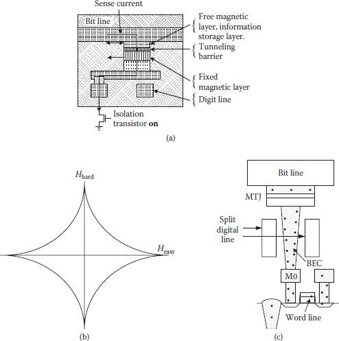
FIGURE 1.17
(a) Diagram of MTJ device in “read” mode with series isolation transistor. (“Recent Developments in Magnetic Tunnel Junction MRAM,” S. Tehrani et al., IEEE Trans. Magnetics, Vol. 36, pp. 2752–2757, 2000.) (b) Ideal switching asteroid. (Redrawn from “Memories of Tomorrow,” W. Reohr et al., IEEE Circuits and Device Magzine, pp. 17–27, Sept. 2002.) (c) 8F2 MRAM cell structure with split digital-line. (Modified from “Future Memory Technology including Emerging New Memories,” K. Kim and G-H. Koh, Proc. 24th Int. Conf. on Microelectronics (MIEL), Vol. 1, pp. 377–384, 2004.)
1.8.3.1 Spin–Torque–Transfer (STT) MRAM
In conventional MRAMs, writing current was a significant limiting factor, which was effectively overcome through the application of spin-torque transfer magnetizing switching (STS). In the STS scheme, instead of providing magnetic field externally, direct injection of spin polarized electrons was used to reverse the direction of magnetic layer. It was also expected that STS current would decrease with downscaling of technology mode.
A memory cell of the STT MRAM is shown in Figure 1.18, which has a source line instead of a digit line of a conventional MRAM. Operationally, the read process is the same; only the write process is modified in which word line is selected and a positive voltage is applied at bit line or source line of a selected column. A 4 kb STT MRAM was fabricated in 0.18 μm CMOS technology which employed an MTJ with CoFeB ferromagnetic layer and crystallized MgO tunnel barrier layer of 1 nm thickness. With the kind of materials used, an MR ratio of more than 160% at RA product of 20 Ωμm2 was obtained [73]. Fabricated STT MRAM proved the practical feasibility of switching driving force from the spin polarized current other than external induced field and exhibited high speed, low power, and high scalability. Fabrication in smaller technology mode would increase read/write speed and integration density. However, a major challenge in this direction is the process variation affects especially in MTJ. Variations in tunneling oxide thickness and the cross-sectional area of the MTJ cause incorrect read and inability in write process that considerably reduce yield of the MRAMs. Efforts have continuously been made for improving device design and process control [74] though without adequate success, in spite of using advanced fabrication technologies. Alternatively, a circuit level solution is suggested for reducing process variation effects. A detailed study concluded that the sizing of the n-channel MOSFET (NMOS) used is important [75]. NMOS wider than minimum size reduces write failure probability but increases read failures and incurs area penalty. Reduction in NMOS size affects conversely. A circuit-based scheme was proposed in which one MTJ, two NMOS transistors, one minimum sized for reading, and another NMOS, a bit larger for writing, were used. With an area overhead of ~9%, reduction in read failure probability was 39% and the reduction in write failure probability was 31% [75].
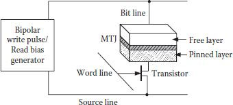
FIGURE 1.18
A schematic STT MRAM memory cell. (Redrawn from “A Novel Nonvolatile Memory with Spin Torque Transfer Magnetization Switching: spin ram,” M. Hosomi et al., IEDM Tech. Dig., pp. 459–462, 2005.)
Another way of looking at the read/write failure probability is from a system-performance perspective. Reads occur more frequently than writes and read operations are directly in the critical path too [76]. A design technique called stretched write cycle (SWC) is employed in which architectural modification is made with write operation consuming one more cycle; hence, the requirement of wider NMOS is relaxed, density is improved, and read failure probability is also reduced.
With continued interest in STT-MRAM bit cell design [77,78,79], low power, less susceptibility to process variation, and reliable memories are highly likely to be available at the high-density level [80].
Compact discs and DVD optical memory discs have extensively used phase change materials. However, a GeSbTe chalcogenide alloy-based memory cell element of an ovonic unified memory (OUM) in 180 nm technology was developed in 2001 [81]. State of the chalcogenide materials changes between being amorphous or crystalline. This change of state is possible with a small amount of heating through the application of a current pulse for a short duration. During amorphous phase, high resistance is offered known as SET state, whereas during crystalline state, low resistance is observed that is known as RESET state, and the difference of resistance in the two states is converted into high and low states of a memory cell. Figure 1.19(a) shows a simplified cross-section of an OUM memory cell element, which is a thin film two-terminal device and can be fabricated using conventional processes. For heating the cell, current pulse of comparatively high value of very short duration (a few ns) is required which melts the chalcogenide material, crystalline nature is totally disturbed and resistance becomes more than 100 kΩ. For conversion to crystalline state, current pulse of comparative small value flows for larger duration (2–50 ns) as shown in Figure 1.19(b), so that enough time is available for crystal growth and resistance becomes less than 1 kΩ.
Because of large resistance difference between two states, sufficient read signal margin becomes available. For the fabricated memory, read/write speed was comparable with contemporary DRAM. Read endurance is unlimited and scaling is mainly dependent on lithography. It is more adaptable for low power because of its low voltage operation [81]. Another OUM 4 Mbit NV memory is realized at 0.18 μm technology node [38]. In a study of its sequential operations, write/read/write complement/read, cycling at 5 MHz, a reset pulse of 8 ns was applied for ~5 ns falling edge and corresponding cell read resistance was found to be 85 kΩ. A set pulse of 85 ns changes the resistance to 2 kΩ showing wide resistance variation practically, and value of Vth at the beginning of set pulse is ~0.6 V. Another distinct advantage of OUM phase change memories is their compatibility with embedded systems because of low temperature processes used after transistor fabrication.
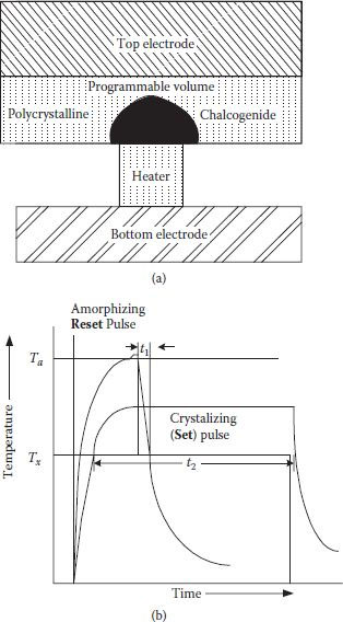
FIGURE 1.19
(a) Simplified cross-section of an ovonic unified memory element. (b) Current pulse width and temperature relationship of the phase change process. (“OUM-A 180 nm Nonvolatile Memory Cell Element Technology for Stand Alone and Embedded Applications,” S. Lai et al., IEDM Tech. Dig., pp. 803–806, 2001.)
There appears to be no scaling constraint in CMOS technology as far as the fabrication process of PRAM is concerned. Problem area is mainly concerned with its practical functionality, like large current consumption during the reset process when chalcogenic material changes to amorphous state. So it requires large size transistor and eventually a larger cell size. Another problem area is the possibility of set resistance increasing when reset current is decreased. As a consequence of large set resistance, read time is increased and noise immunity is reduced [45]. For reducing reset current, techniques used are modification in GST material and the cell structure, and reduction in cell dimensions. The PRAMs have an advantage that with the cell size reduction, reset current can be scaled down.
Not only to prove the manufacturability of PRAM but also to enhance its performance, a novel structure was given by Pellizzer and others [82], which was CMOS technology-compatible, had faster read/write access time and programming current was also reduced. The important concept used here was that of μTrench, the formation of a trench in which GST is deposited and a thin vertical semimetallic heater as shown in Figure 1.20. A common collector p-n-p BJT access device in vertical cell architecture was realized which results in a compact cell area of 10 F2 (0.32 μm2 at 0.8 μm CMOS technology). Proposed μTrench structure helps in reducing the programming current to 600 μA and endurance of 1011 programming cycles. Vertical salicided p-n-p BJT with the storage element comprising of heater and chalcogenide material on top is fabricated at 90 nm technology [83]. Smaller contact area of the μTrench heater reduces the programming current to 400 μA. Using a simple layout with one base contact for every emitter, cell size of 0.096 μm2 (equivalent to 12 F2) is obtained. A similar approach at 45 nm technology, but with one base contact with every four emitters has reduced the cell size to 5.5 F2 (.015 μm2) [84] while developing 1 Gbit PRAM for the first time.
FIGURE 1.20
Schematic cross-sections of the basic structure of PRAM. (“Novel μTrench Phase-Change Memory Cell for Embedded and Stand-Alone Non-Volatile Memory Applications,” F. Pellizzer et al., Symp. VLSI Tech. Dig. Tech. Papers, pp. 18–19, 2004.)
A Comparison of Important Next-Generation Nonvolatile Memories
FRAM (Ferroelectric) |
MRAM (Magnetic) |
PCM (Phase Change) |
|
Storage mechanism |
Permanent polarization of a ferroelectric material like PZT |
Permanent magnetization of ferromagnetic material in a MTJ |
Amorphous/polycrystal phases of chalcogenide alloy |
Cell size (F2) |
~20 |
~20 |
~6 |
Scalability |
Poor |
Poor |
Good |
Endurance |
1010 |
>1014 |
1012 |
Application |
Embedded, low density |
Embedded, low density |
Stand-alone, or embedded high density |
Source: “Phase Change Memory: Development Progress and System Opportunities,” G. Atwood, Interconnect Technology Conference (IITC), International, pp. 1–3, 2010.
With small contact area, μTrench structure is very suitable in reducing the reset current; however, it requires lithography to define the GST dimension and making a small contact for the underlying metal. A cross-spacer phase change memory cell has been developed which provides lithography-independent contact area that is very small (~1000 nm2) resulting in reduced reset current of 230 μA [85]. As already mentioned, reduction of reset current is an important area and further investigations are to continue toward the wall heater approach [82]. In addition, finding new chalcogenide material other than GST is also an important research area.
It is desirable to compare important alternative emerging NV memories. Few characteristics have been included in Table 1.1 [86], which may be helpful in selecting a suitable memory for an application.
1. J.M. Rabaey, A. Chandrakasan, and B. Nikolic, Digital Integrated Circuits: A Design Perspective, Pearson, Prentice Hall, 2003.
2. M. Takada and T. Enomoto, “Review and Prospects of SRAM Technology,” Trans. IEICE, Vol. E74, pp. 827–839, 1991.
3. S.M. Kang and Y. Leblebici, CMOS Digital Integrated Circuits—Analysis and Design, Tata McGraw-Hill, 2003.
4. V.L. Rideout, “One-Device Cells for Dynamic Random Access Memories: A Tutorial,” IEEE Trans. Electr. Dev., Vol. ED-26, pp. 839–852, 1979.
5. R.C. Foss, “The Design of MOS Dynamic RAMs,” IEEE ISSCC. Tech. Dig., p. 140, 1979.
6. N.-C. Lu and H.H. Chao, “Half-VDD Bit-Line Sensing Scheme in CMOS DRAMs,” IEEE J. Solid State Circuits, Vol. SC-22, pp. 451–454, 1984.
7. K.U. Stein, A. Sihling, and E. Doering, “Storage Array and Sense/Refresh Circuit for Single Transistor Memory Cell,” IEEE Int. S.S. Circuits Conf., pp. 56–57, 1972.
8. Y. Katayama, “Trends in Semiconductor Memories,” IEEE Micro, pp. 10–17, 1997.
9. B. Prince, High Performance Memories, John Wiley and Sons, Chapter 2, 1999.
10. B. Prince, “Application Specific DRAMs Today,” Proc. Int. Workshop on Memory Technology, Design, and Testing (MTDT), 2003.
11. A.B. Cosoroaba, “Double Data Rate SYNCHRONOUS DRAMs in High Performance Applications,” Proc. IEEE WESCON Conf., 1997.
12. Y. Choi et al., “A 16 Mbit Synchronous DRAM with 125 Mbytes/sec Data Rate,” VLSI Circuits Symp. Dig., pp. 65–66, 1993.
13. Y. Takai et al., “250 Mbyte/sec Synchronous DRAM Using 3-Stage-Pipelined Architecture,” VLSI Circuits Symp. Dig., pp. 59–60, 1993.
14. Elpida Corporation, “DDR II 512 M SDRAM Specification,” 2002.
15. H. Fujisawa et al., “1.8-V 800-Mb/s/pin DDR2 and 2.5-V 400-Mb/s/pin DDR1 Compatibly Designed 1 Gb SDRAM with Dual Clock Input Latch Scheme and Hybrid Multi-Oxide Output Buffer,” Symp. VLSI Circuits, Dig. Tech. Papers, pp. 38–39, 2004.
16. Y.K. Kim et al., “A 1.5 V, 1.6 Gb/s/pin, 1 Gb DDR3 SDRAM with an Address Queuing Scheme and Bang-Bang Jitter Reduced DLL Scheme,” Symp. VLSI Circuits, Dig. Tech. Papers, pp. 182–183, 2007.
17. T.-Y. Oh et al., “A 7 Gb/s/pin 1 Gbit GDDR5 SDRAM with 2.5 ns Bank to Bank Active Time and Ni Bank Group Restriction,” IEEE. J. Solid State Circuits, Vol. 46, pp. 107–118, 2010.
18. Ashok K. Sharma, Semiconductor Memories, Technology, Testing, and Reliability, IEEE Press, 1997.
19. K. Bernstein and N.J. Rohrer, SOI Circuit Design Concepts, Springer Science, 2007.
20. K. Suma et al., “An SOI-DRAM with Wide Operating Voltage Range by CMOS/SIMO Technology,” IEEE ISSCC Tech. Dig., pp. 138–139, 1994.
21. S. Kuge et al., “SOI-DRAM Circuit Technology for Low Power High Speed Multi-Giga Scale Memories,” VLSI Circuits Symp. Dig., pp. 103–104, 1995.
22. S. Okhonin et al., “A SOI Capacitor-less 1-T DRAM Concept,” Proc. IEEE. Int. Conf., pp. 153–154, 2001.
23. S.K. Moore, “Masters of Memory,” IEEE Spectrum, pp. 45–49, 2007.
24. H.J. Wann and C. Hu, “A Capacitor-less DRAM cell on SOI Substrate,” IEDM Tech. Dig., pp. 635–638, 1993.
25. T. Tanaka, E. Yoshida, and T. Miyashita, “Scalability Study on a Capacitor-less 1T-DRAM: From Single-Gate PD-SOI to Double Fin DRAM,” IEDM Tech. Dig., pp. 919–922, 2004.
26. C. Kuo, T.-J. King, and C. Hu, “A Capacitor-less Double-Gate DRAM Cell,” IEEE Electr. Dev, Lett., Vol. 23, pp. 345–347, 2002.
27. E. Yoshida, T. Miyashita, and T. Tanaka, “A Study of Highly Scalable DG-Fin DRAM,” IEEE Electr. Dev. Lett., Vol. 26, pp. 655–657, 2005.
28. C. Kuo, T.-J. King, and C. Hu, “A Capacitorless Double-Gate DRAM Cell Design for High Density Applications,” IEDM Tech. Dig., pp. 843–846, 2002.
29. I. Ban et al., “Floating Body Cell with Independently-Controlled Double Gates for High Density Memory,” IEDM Tech. Dig., pp. 1–4, 2006.
30. M.G. Ertosun et al., “A Nanoscale Vertical Double-Gate Single-Transistor Capacitorless DRAM,” IEEE Electr. Dev. Lett., Vol. 29, pp. 615–617, 2008.
31. M. Bawedin et al., “A Capacitorless 1T-DRAM on SOI Based on Dynamic Coupling and Double-Gate Operation,” Electron. Dev. Lett., Vol. 29, pp. 795–798, 2008.
32. S.-W. Ryu et al., “Unified Random Access Memory (URAM) by Integration of a Nano Crystal Floating Gate for Nonvolatile Memory and a Partially Depleted Floating Body for Capacitorless 1-T DRAM,” Solid State Electronics, Vol. 53, pp. 389–391, 2009.
33. J.-W. Han et al., “Partially Depleted SONOS FinFET for Unified RAM (URAM)-Unified Function for High-Speed 1T DRAM and Nonvolatile Memory,” IEEE Electron. Dev. Lett., Vol. 29, pp. 781–783, 2008.
34. J.-Y. Lin et al., “Performances of a Capacitorless 1R-DRAM Using Polycrystalline 1T-DRAM Using Polycrystalline Silicon Thin-Film Transistors with Trenched Body,” IEEE Electr. Dev. Lett., Vol. 29, pp. 1222–1225, 2008.
35. Y. Yatsuda et al., “Hi-MNOS II Technology for a 64 Kbit Byte-Erasable 5V only EEPROM,” IEEE J. Solid-State Circuits, Vol. SC-20, p. 144, 1985.
36. J.T. Evans and R. Womack, “An Experimental 512-bit Nonvolatile Memory with Ferroelectric Storage Cell,” IEEE J. Solid State Circuits, Vol. 23, pp. 1171–1175, 1988.
37. J.M. Daughton, Thin Film Magnetic RAM Devices, Honeywell Inc., 1988.
38. M. Gill et al., “Ovonic Unified Memory—A High Performance Nonvolatile Memory Technology for Stand-Alone Memory and Embedded Applications,” ISSCC Tech. Dig., pp. 202–204, 2002.
39. R. Pashley and S. Lai, “Flash Memories: The Best of Two Worlds,” IEEE Spectrum, pp. 30–33, 1989.
40. M. Momodami et al., “An Experimental 4-Mbit CMOS EEPROM with a NAND Structure Cell,” IEEE J. Solid State Circuits, pp. 1238–1243, 1989.
41. K. Itoh, VLSI Memory Chip Design, Springer-Verlog, 2001.
42. S. Pawan et al., “Flash Memory Cell—An Overview,” Proc. IEEE, Vol. 85, pp. 1248–1271, 1997.
43. R. Bez et al., “Introduction to Flash Memory,” Proc. IEEE, Vol. 91, pp. 489–502, 2003.
44. H.-H. Tseng et al., “ALD HfO2 Using Heavy Water (D2O) for Improved MOSFET Stability,” IEDM Tech. Dig., pp. 83–86, 2003.
45. K. Kim and G.-H. Koh, “Future Memory Technology including Emerging New Memories,” Proc. 24th Int. Conf. on Microelectronics (MIEL), Vol. 1, pp. 377–384, 2004.
46. J.D. Lee et al., “Effects of Floating-Gate Interference on NAND Flash Memory Cell Operation,” Electr. Dev. Letters, Vol. 23, pp. 264–266, 2002.
47. C.H. Lee et al., “A Novel SONOS Structure of SiO2/SiN/Al2O3 with TaN Metal Gate for Multi-giga Bit Flash Memories,” IEDM Tech. Dig., pp. 613–616, 2003.
48. Yan Li et al., “A 16 Gb 3b/cell NAND Flash Memory in 56 nm with 8 MB/s Write Rate,” ISSCC Tech. Dig., pp. 506–507, 2008.
49. H. Kurata et al., “Constant-Charge-Injection Programming for 10-MB/s Multilevel AG-AND Flash Memories,” VLSI Circuits Symp. Dig., pp. 302–303, 2002.
50. N. Shibata et al., “A 70 nm 16 Gb 16-Level-Cell NAND Flash Memory,” VLSI Circuit Symp. Dig., pp. 190–191, 2007.
51. T. Nozaki et al., “A 1 Mbit EEPROM with MONOS Memory Cell for Semiconductor Disc Application,” VLSI Circuit Symp., pp. 101–102, 1990.
52. K. Kim, “Future Memory Technology: Challenges and Opportunities,” Int. Symp. VLSI Technology, Systems, and Applications (VLSI-TSA), pp. 5–9, 2008.
53. C.B. Kim et al., Memory Cell Capacitor Using Cross Double Patterning Technology for Gigabit Density DRAM, ISDRS, 2009.
54. Y.C. Shin et al., “A Novel NAND-Type MONOS Memory Using 63 nm Process Technology for Multi-gigabit Flash EEP ROMs,” IEDM Tech. Dig., pp. 327–330, 2005.
55. Y. Park et al., “Highly Manufacturable 32 Gb Multi-Level NAND Flash Memory with 0.0098 μm2 Cell Size Using TANOS (Si oxide-Al2O3-TaN) Cell Technology,” IEDM Tech. Dig., pp. 29–32, 2006.
56. D. Kwak et al., “Integration Technology of 30 nm Generation Multilevel NAND Flash for 64 Gb NAND Flash Memory,” VLSI Tech. Dig., pp. 12–13, 2007.
57. E.-L. Lai et al., “A Multilayer Stackable Thin-Film Transistor (TFT) NAND Type Flash Memory,” IEDM Tech. Dig., pp. 37–40, 2006.
58. Y. Fukuzumi et al., “Optical Integration and Characteristics of Vertical Array Devices for Ultra-High Density, Bit-Cost Scalable Flash Memory,” IEDM Tech. Dig., pp. 449–452, 2007.
59. W.A. Geideman et al., “Progress in Ferroelectric Memory Technology,” IEEE Trans. Ultrason., Ferr., Freq. Contr., Vol. 38, 1991.
60. T. Miyazaki and N. Tezuka, “Giant Magnetic Tunneling Effect in Fe/Al2O3/Fe Junction,” J. Magn. Mater., Vol. 139, L231, 1995.
61. W.J. Gallagher et al., “Microstructured Magnetic Tunnel Junction,” J. App. Phy., Vol. 81, pp. 3741–3746, 1997.
62. M.N. Babich et al., “Giant Magnetoresistance of (100) Fe/(001) Cr Magnetic Superlattices,” Phy. Rev. Lett., Vol. 61, pp. 2742–2745, 1988.
63. J.M. Slaughter, E.Y. Chen, and S. Tehrani, “Magnetoresistance of Ion-Beam Deposited Co/Cu/Co and NiFe/Co/Cu/Co/NiFe Spin Valves,” J. App. Phys., Vol. 85, pp. 4451–4453, 1999.
64. S. Tehrani et al., “High Density Nonvolatile Magnetoresistance RAM,” IEDM Tech. Dig., pp. 193–196, 1996.
65. S. Tehrani et al., “Progress and Outlook for MRAM Technology,” IEEE Trans. Magnetic, Vol. 35, pp. 2814–2819, 1999.
66. S. Tehrani et al., “Recent Developments in Magnetic Tunnel Junction MRAM,” IEEE Trans. Magnetics, Vol. 36, pp. 2752–2757, 2000.
67. W. Reohr et al., “Memories of Tomorrow,” IEEE Circuits and Device Magazine, pp. 17–27, Sept. 2002.
68. S. Tehrani et al., “Magnetoresistive Random Access Memory Using Magnetic Tunnel Junctions,” Proc. IEEE, Vol. 91, pp. 703–713, 2003.
69. M. Motoyoshi et al., “High Performance MRAM Technology with an Improved Magnetic Tunnel Junction Material,” VLSI Tech. Dig., pp. 212–213, 2002.
70. M. Durlam et al., “A 0.18 μm 4 Mb Toggling MRAM,” IEDM Tech. Dig., pp. 995–997, 2003.
71. M. Durlam et al., “A Low Power 1 Mbit MRAM Based on 1M 1MTJ Bit Cell Integrated with Copper Interconnects,” VLSI Circuits Dig. Tech. Papers, pp. 158–161, 2002.
72. M. Durlam et al., “A 1 Mbit MRAM Based on 1 T 1 MTJ Bit Cell Integrated with Copper Interconnects,” J. Solid State Circuits, Vol. 38, pp. 769–773, 2003.
73. M. Hosomi et al., “A Novel Nonvolatile Memory with Spin Torque Transfer Magnetization Switching: Spin RAM,” IEDM Tech. Dig., pp. 459–462, 2005.
74. M. Motoyoshi et al., “A Study for 0.18 μm High-Density MRAM,” VLSI Symp. Dig. Tech. Papers, pp. 22–23, 2004.
75. J. Lee et al., “Variation-Tolerant Spin-Torque Transfer (STT) MRAM Array for Yield Enhancement,” IEEE Custom Int. Circ. Conf., pp. 193–196, 2008.
76. P. Ndai, A. Goel, and K. Roy, “A Scalable Circuit Architecture Co-Design to Improve Memory,” IEEE Trans. VLSI, Vol. 18, pp. 1209–1219, 2010.
77. C.J. Lin et al., “45 nm Low Power CMOS Logic Compatible Embedded STT MRAM Utilizing a Reverse-Connection 1T/1MTJ Cell,” IEDM Tech. Dig., pp. 279–282, 2009.
78. T. Kawahara et al., “2 Mb Spin-Transfer Torque RAM (SPRAM) with Bit-by-Bit Bidirectional Current Write and Parallelizing-Direction Current Read,” Proc. ISSCC, pp. 480–482, 2007.
79. J. Li et al., “Design Paradigm for Robust Spin-Torque Transfer Magnetic RAM (STT MRAM) from Circuit/Architecture Perspective,” IEEE Trans. VLSI, pp. 1710–1723, 2008.
80. C. Augustine et al., “Spin-Transfer Torque MRAMs for Low Power Memories: Perspective and Prospective,” IEEE Sensor Journal, 2011.
81. S. Lai et al., “OUM-A 180 nm Nonvolatile Memory Cell Element Technology for Stand Alone and Embedded Applications,” IEDM Tech. Dig., pp. 803–806, 2001.
82. F. Pellizzer et al., “Novel μTrench Phase-Change Memory Cell for Embedded and Stand-Alone Non-Volatile Memory Applications,” Symp. VLSI Tech. Dig. Tech. Papers, pp. 18–19, 2004.
83. F. Pellizzer et al., “A 90 nm Phase Change Memory Technology for Stand-Alone Non-Volatile Memory Applications,” Symp. VLSI Tech. Dig. Tech. Papers, 2006.
84. G. Servalli, “A 45 nm Generation Phase Change Memory Technology,” IEDM Tech. Dig., pp. 113–116, 2009.
85. W.S. Chen et al., “A Novel Cross-Spacer Phase Change Memory with Ultra-Small Lithography Independent Contact Area,” IEDM Tech. Dig., pp. 319–322, 2007.
86. G. Atwood, “Phase Change Memory: Development Progress and System Opportunities,” Interconnect Technology Conference (IITC), International, pp. 1–3, 2010.