Low cost per bit and high packing density of DRAMs are unmatched by any other semiconductor memory. Within the limitations of fabrication processes, mainly lithography, area of the memory cell layout is very crucial as it has direct impact on the performance and the cost. The initial-stage cell was a simpler entity, of course, in comparison to the complex products of today, in the form of a single access transistor and a storage capacitor laid side by side in two dimensions; it has been called a planar DRAM cell. Overall cell size continued to shrink without any serious obstacles till the 1–4 Mbit range. However, beyond that, shrinking of the cell in two dimensions became impracticable, because planar capacitor alongside access transistor could not hold sufficient charge (or realize enough capacitance) in a small area. Sizing of the transistors was also going to be a challenge with shrinking the cell, but it was a delayed factor at a much lower minimum feature size of around 100 nm. Different alternatives were used while making the cell three-dimensional. One approach was the stacked capacitor cell in which the capacitor was realized on top of the switching transistor. Cells in which the capacitor was fabricated in the substrate came to be known as trench capacitors cells. Varieties of both the stacked capacitor and the trench capacitor cell came into practice.
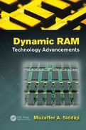
Single transistor memory cell at the initial stage consisted of a MOSFET switch and a charge storage capacitor as shown in Figure 2.1(a), where total storage consisted of two capacitances: Cjn (junction capacitance) and a bias-independent MOS capacitance Cox, which was normally 5 to 10 times larger than Cjn [1]. The storage capacitor electrode which connects to the MOSFET source could be either an n-type diffused region or an inversion layer (of electrons for p-substrate in NMOS), as shown in Figure 2.1(b) and (c), respectively. The charge storage capacitor remains (1) in the neutral/stable 0 state while having electrons normally present in n-type doped region as shown in Figure 2.1(b) or in a surface inversion layer under a biased plate electrode as shown in Figure 2.1(c) or (2) in the charged/unstable 1 state by removing electrons through the MOSFET switch. Leakage current through the MOSFET very quickly restores electrons in the 1 state, converting it to the 0 state; hence, removal of these charges or refreshing is a must.
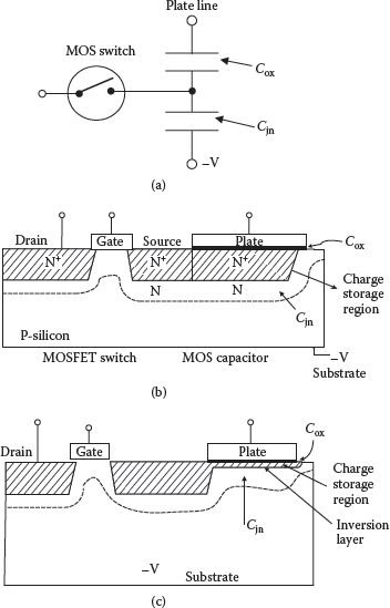
FIGURE 2.1
Planar transistor memory cell. (a) Equivalent circuit, basic structure (b) with diffusion storage, and (c) with inversion storage. (Redrawn from “One-Device Cells for Dynamic Random—Access Memories: A Tutorial,” V.L. Rideout, IEEE Trans. Electr. Dev. Vol. 26, pp. 839–852, 1979.)
During the evolutionary phase of the above-mentioned planar one-transistor DRAM (1T DRAM), several modifications and forms of realizations were found feasible. As the DRAM size increased from 4/16 Kbit to 64 Kbit and then to 1 Mbit per chip, cell structure changed its form due to (1) various MOSFET technologies, and (2) arrangement of the bias and control lines to drain, gate and capacitor plate, and storage capacitor formation itself along with few variations as well in each entity. Details of MOSFETs are discussed in Chapter 4, for advanced MOSFETs, as the conventional two-dimensional MOSFET theory and fabrication process is already well studied. During DRAM development stages two important figures of merit for a DRAM cell were/are given due importance. A number of lithographic squares (i.e., a square whose side equals the minimum feature size) consumed by the cell and the charge transfer ratio, as given in Chapter 1 generally in the range of 5 to 20, form a performance figure of merit [2]. However, other figures of merit like processing complexity (number of lithographic masking operations, etching steps, and high temperature treatments), chip performance (access/cycle time, refresh period, and power dissipation), and cost (chip size, yield, and packaging), must also be considered. Based on the consideration of all figures of merit, enumerated above, it was clear as early as 1979 that polysilicon-to-polysilicon (poly-to-poly or double-poly) storage capacitor [3] shall be a suitable structure for planar cell configuration. It was verified later by many researchers that such a cell was indeed very suitable, however, only up to the 1 to 4 Mbit density level [2].
It is important to know the reasons behind more innovative cell/capacitor structures/organizations involving relatively difficult processing option like a double-poly planar cell. Figures 2.2(a) and (b) show the cross-section of the double-poly planar cell structure and its equivalent circuit representation. Here, VBL, VWL, and VSP are the voltages applied at the bit line, word line, and the storage plate, respectively. Charge transfer between the bit line and the storage region takes place when the word line is high. The access transistor gate has a higher threshold voltage compared to that of the storage region and its effect is that when word line is high the surface potential below the transfer gate is lower than both the electrostatic potentials of the bit line and the storage area for the same applied voltage to these regions [4].
FIGURE 2.2
(a) Cross-section of a double poly one-transistor DRAM cell and modification (within dotted line) to convert as H-C cell and (b) circuit representation. (Redrawn from “Design Parameters of the Hi-C DRAM Cell”, Y.A. EL-Mansy and R.A. Burghard, IEEE. J.S.S. Circuits, Vol. SC-17, pp. 951–956, 1982.)
It is observed that the amount of charge Q in the storage region corresponding to low-state, Q (low), for a full-charge well, is a function of Cos, the oxide capacitance per unit area for the storage region; NB, bulk doping concentration; Pf, the surface potential corresponding to full charge well; and VSP. The charge Q remaining in the storage area corresponding to an empty-cell, Q (high) is a function of Cos, NB, VSP, and Pe, the surface potential in the transfer gate region at gate voltage VWL. So, the maximization of charge signal ΔQ = Q(low) – Q(high) for a given storage area (or increasing the storage charge capacity) is done through, (1) increase of Cos, (2) reduction in threshold voltage in the storage gate area, and Pf, and (3) increase of Pe. Increase in the depletion capacitance CD through increase of bulk doping concentration NB is another option. All these options effectively require reduction of oxide thickness both at the storage and the transfer gate region, and reduced doping concentration below the storage gate. Obviously, reduction in SiO2 thickness could be attempted up to a certain minimum level. Even if breakdown does not occur, carriers can pass through very thin oxide layer. Increase in permittivity through use of another dielectric was not given a consideration at that stage, which later became a strong point. The other option was to increase CD, which required an increase in the doping concentration below the storage gate—a requirement contradictory to the earlier options, as it reduces storage gate threshold voltage. A modified Hi-C cell was introduced to satisfy both the requirement of increasing the substrate doping in the storage area for high depletion capacitance while maintaining low threshold voltage by Sodini and Kamins [5] and by Tasch et al. [6]. A boron layer is implanted in the storage area to increase substrate doping (and hence increases CD); then the resulting increase in threshold voltage is offset by implanting a layer of n-type impurities at the surface shown as modification in Figure 2.2. The Hi-C cell has also been shown to operate with grounded plate (Vsp = 0), which is desirable for high-density memory chips.
The packing density and capacity of 1T DRAM cells continued to increase in conformity with the device scaling theory of Dennard [7]. It was predicted as early as 1975 that planar MOS capacitor 1T cell with a two-dimensional structure would encounter following problems:
1. Scaling down limitation is serious because MOS capacitor area could not be scaled down to have minimum signal charge ΔQ in the range of 200 fC corresponding to the storage capacitance of 65 fF at VDD of 3.3 V. With scaled-down insulator thickness of 10 nm, estimated needed capacitor area was approximately 20 μm2, which was about twice the cell area for a 4 Mbit DRAM chip of 75 mm2, for which cell area has to be below 10 um2 (assuming ~60% of the chip area earmarked for the core).
2. Another problem of a serious nature was in the form of signal reduction due to the minority carriers generated in the silicon substrate. This occurs because the charges in the inversion layer and the depletion layer of the storage capacitor are affected by the minority carriers, which are thermally or optically generated, or generated by the irradiation of cosmic rays like alpha particles.
3. Fabrication of access transistor, whether by the side of storage capacitor, on top of it, or below it, was also going to be a serious problem, with increasing DRAM density and shrinkage of minimum feature size. To keep transistor performance as per requirements, DRAM cell was also going to be three-dimensional, thereby changing its shape drastically.
As a result of the number of fabrication and operational difficulties mentioned, further advancement in DRAM density was not possible beyond 1–4 Mbit using the planar DRAM cell. Higher density 1T DRAMs were realized through innovation in cell design, mainly through various forms of three-dimensional capacitors and cells, such as trench and stacked structure, at least up to 1 Gbit density level. Be it trench or stacked capacitor, capacitance had to be enhanced without increasing projected area (in fact area was to be decreased) with increasing DRAM density. Schemes for the capacitance enhancement are discussed in Chapter 5, whereas development of a few early stage three-dimensional cells is discussed in the following sections. First-generation trench capacitor cells laid the foundation of the fabrication of capacitors below the surface of the wafer. Various kinds of the first-generation trench capacitors have been discussed in Section 2.3.1. To save the trench capacitors from likely intercell punch-through and for the minimization of the effects of cosmic ray irradiation inverted trench capacitor cells were realized. These cells, which kept the storage node inside a trench, are discussed in Sections 2.3.2 and 2.6. In almost all such cells access transistor was fabricated by the side of the trench capacitor which consumed chip area. A modified cell structure in which chip area is saved by fabricating access transistor above the trench capacitor is given in Section 2.4. Section 2.5 describes a DRAM cell in which both the vertical transistor and storage capacitor are realized in a trench. In late 1980, fabrication of vertical transistor was not mature and few cells were fabricated with planar transistors and capacitors buried under them. However, a popular choice for higher density DRAM became available in the form of stacked capacitor cells in which storage capacitor was stacked above the access transistor. Stacked capacitor cell basics and some variations are discussed in Section 2.8. Though their properties, characteristics, and advantages like using metal-insulator-metal (MIM) form capacitor and/or capacitor-over-bit line (COB) structure are discussed in Chapter 6.
2.3 Three-Dimensional Capacitor DRAM Cell
Exceeding a 4 Mbit conventional planar access transistor and a planar capacitor in a two-dimensional structure was highly unpractical so cell structures had to use advanced processing techniques to meet the design criteria. It became necessary to move toward a third dimension for the capacitor as well as for the cell structure. As mentioned before, main categorization was in terms of trench or stacked form. First, trench capacitor cells of the first generation, that have storage plates of the capacitor outside the insulated trench are described.
2.3.1 First-Generation Trench Capacitor Cell
As the name suggests, storage of charge is done in a trench that is below the surface level and inside the substrate in trench capacitor cell, thereby reducing the projected area of the capacitor. Although this kind of structure was attempted in vertical MOS (VMOS) DRAM [8,9] earlier, it did not succeed due to the sharp edges at the bottom, which resulted in the thinning of the gate oxide at corners, making it unmanufacturable. The main reason for this problem in VMOS structure was the use of orientation based etching. Whereas reactive ion etching (RIE) was used in the realization of trench capacitor with breakdown characteristics similar to the planar capacitor. Attempts were made to get better performance with a combination of trench etch control, edge rounding technique and the use of the dielectrics which were a combination of thermal and deposited layers [10]. However, the first reports on manufacturable trench capacitor appeared in 1982–83 [11,12] in the form of corrugated capacitor cells, which are discussed in the following section. A few more first-generation trench capacitor cells are then discussed.
2.3.1.1 Corrugated Capacitor Cell
Sunami [11] gave the concept and structure of a corrugated capacitor cell (CCC) having a capacitor formed in a dry etched moat into silicon substrate but a more physically realizable trench cell form was given later which is shown in Figure 2.3 [10]. As the trench capacitor stores charge along the outside walls as well as at the bottom of the trench, the storage area is greatly enhanced with even reduced planar projected surface for the capacitor. The main advantage of the trench idea was that by simply increasing the depth of the trench, capacitance could be increased. Obviously, the fabrication of a huge number of uniformly etched trenches was a challenge without having dielectric breakdown. However, the objective was successfully achieved [13] and 1 Mbit to 4 Mbit DRAM chips using trench capacitor were realized. Modified and improved versions of trench capacitor cells have also been successfully manufactured, in spite of the fact that some design concerns were expressed in the original trench capacitor structure of ref. [11]. A major concern was that as the charge was stored around the trench surface in the substrate silicon, the larger storage areas became highly susceptible to minority carrier leakage and prone to high soft error rate (SER). High-leakage currents could also arise between adjacent trenches and the active device of the next cell due to the punch-through or surface conduction. Furuyama et al. suggested a solution of the problem in an experimental 4 Mbit DRAM [14]. To make the cell less susceptible to soft errors due to the irradiation of the α-particles, an n-channel depletion type trench cell is fabricated in a p-well on a p-substrate similar to the one in Figure 2.3. In addition, p-well impurity concentration was increased that narrowed down the depletion region and suppressed leakage current between adjacent cells. With increased doping concentration, leakage is reduced but it was likely to cause avalanche breakdown. Trench spacing was limited by the diffusion depths of doping profiles and depletion regions. Another option used was to make a deeper trench, however, these were difficult to fabricate, hence more problematic. The problem of leakage in a deep trench was solved to some extent in a 4 Mbit DRAM by T. Sumi et al. [15] that is shown in a cross-sectional view of the cell (Figure 2.4). In deep trench capacitors, the bottom of the electrode is more susceptible to leakage on account of lower p-well concentration. To overcome it, arsenic was doped at the sides and bottom of the trench to form N-type regions, preventing the decrease in memory cell capacitance. In addition, boron was doped to form a Hi-C structure. A memory cell of 8.0 μm2 (1.7 μm × 4.6 μm) with a 40 fF as capacitance and a 4 μm trench depth was fabricated which could suppress leakage current between the adjacent cells even at Vcc = 7 V.
FIGURE 2.3
Trench capacitor cell (CCC-Hitachi). (“Trench and Compact Structures For DRAM’s”, P. Chaterji et al., Proc. IEDM, pp. 128–131, 1986.)
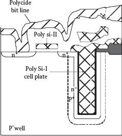
FIGURE 2.4
Cross-sectional view of a deep trench cell. (Adapted T. Sumi et al., “A 60 ns 4Mb DRAM in a 300 mil DIP,” ISSCC Dig. Tech. Papers, pp. 282–283, 1987.)
To maintain required capacitance for higher-density DRAM, the trench needs to be made deeper in CCC, giving rise to the leakage problem via punch-through between neighboring trenches, in addition to the practical problem of etching a deeper trench and suffering from high SER. To minimize the problems cell structures where the trench also serves part of the isolation function have been proposed. One such practical realization for this purpose is a folded capacitor cell (FCC). Instead of using the four sidewalls and bottom of the trench capacitor for charge storage, it was proposed to make the storage capacitor on the vertical wall of a long trench [16]. Increase in the surface area is achieved by folding the capacitor of the conventional trench cell over the isolation edge. The FCC could increase the storage capacitance considerably, therefore, it was then used for realizing larger-density DRAMs. Neighboring capacitors were effectively shielded from each other by high-threshold voltage transistors formed at the bottom; hence, capacitors could be placed closer to each other.
2.3.1.3 Vertical Capacitor Cell
Another trench capacitor with a design similar to that of FCC is a vertical capacitor (VC) cell, which has been realized by Furuyama and Frey [17]. As shown in Figure 2.5, storage MOS capacitor is located vertically only on one sidewall of the trench. Another trench filled with SiO2 and orthogonal to the first provides field isolation between cells. In addition, the bottom part of the trench also isolates capacitors of the neighboring cell, similar to FCC. The VC cell has been shown to have advantage in comparison to a conventional trench cell, in terms of capacitor area and cell area as a function of minimum feature size F. The cell is shown to work satisfactorily for the realization of 16 Mbit DRAM on a 100–120 mm2 chip with a 0.5 μm process, a 2 μm deep trench, and a 6.0 nm thick oxide or equivalent insulator for the capacitor.
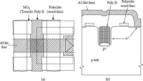
FIGURE 2.5
(a) Top view and (b) cross-sectional view of a vertical cell. (Adapted from T. Furuyama and J. Frey, “A Vertical Capacitor Cell for ULSI DRAMs,” Symp. on VLSI Tech. Dig. Tech. Papers, pp. 16–17, 1984.)
2.3.1.4 Isolation-Merged Vertical Capacitor and Buried Isolation Capacitor Cells
Similar to the FCC cell, merging of storage node and isolation is done in isolation-merged vertical capacitor (IVEC) cells [18,19]. As shown in Figure 2.6, the storage node is a poly layer inside the trench instead of being housed in bulk silicon, improving on soft error rate. Both the storage and the plate electrodes are in a grid-type trench surrounding the access transistor. The storage capacitance is large, but parasitic channel sidewall leakage can increase due to a gated-diode structure across the ends of the device channel [18]. Cell process is complex and provision of layer of high dielectric insulator may be difficult between poly layers. First 16 Mbit DRAM using IVEC was realized occupying 4.9 μm2 area in 0.7 μm technology involving 20 masking steps [19]. Overcoming some of the limitations of IVEC, like avoiding the possible sidewall leakage or sacrificing some performance like having a little less capacitance, similar cells have been realized, such as the surrounding Hi-C capacitance cell in a 4 Mbit chip [20].
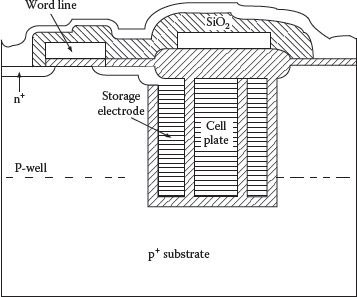
FIGURE 2.6
Cross-section of an isolation-merged vertical capacitor cell. (Redrawn from “Advanced cell structures for dynamic RAMs”, N.C.C. Lu, IEEE Circuits and Devices Magazine, pp. 27–36, Jan. 1989.)
The basic concept of merging the capacitor and isolation region into a buried capacitor formed in a trench is applied in another cell by Nakamura et al. [21]. In the buried isolation capacitor (BIC), cell sidewall of the trench and the polysilicon buried within the trench form two plates of the capacitor. The structure is free from punch-through between adjacent cells; thus, a memory cell of nearly 7 μm2 was realized in 0.8 μm technology, which could make the production of 4 Mbit chip practical. Storage capacitor in each cell is formed on a part of the trench sidewall, which surrounds every two-bit cell periphery, reducing considerably its horizontal surface area. A B+ implantation is done into the bottom of the trench to provide isolation between adjacent cells and silicon dioxide is filled into the trench to complete the fabrication.
In all the implementations where merging of isolation and capacitor is done in a trench, like FCC, IVEC, BIC, and so on, some walls of the trench must act as the cell capacitor while other walls of the trench must act as insulator. Charging (discharging) of the capacitor is done from one edge of the trench as sidewalls are otherwise used; hence, all parasitic paths from the other edges of the trench must be plugged. Different methods were used to achieve this objective such as selective oxidation of the bottom of the trench. Filling different walls of the trench with polysilicon and oxide was the technique employed in the first generation of these cells. The second generation of these cells has employed ion implantation at an angle to selectively dope different faces of the trenches depending on applications [22,23]. Use of these techniques provides some flexibility in reducing/increasing the trench depth.
An advanced 4-MBit density DRAM has been realized occupying 72.3 mm2 chip area, using 0.8 μm design rule, in which different faces of the trenches have been selectively doped forming a folded bit line adaptive side-wall isolator capacitance (FASIC) cell [22,23]. FASIC cell achieves effectively larger sidewall area in a grid-type trench structure as shown in Figure 2.7 and uses several advanced processing steps such as oblique implantation and deep isolation with groove refill. Using oblique implantation, shallow n+ junction at the sidewall is formed uniformly and the junction depth can be controlled by ion beam incident angle. Shallower junction depth depresses the collection of excess electron by 40%. The isolation characteristics of cell are excellent with parasitic leakage current being nearly of the same order as that of a planar memory cell. Formation of cell plate is easier than conventional isolation-merged cell as it is formed on a planar area rather than in the bottom of the trench. However, the cell needs higher number of masks and some signal charge is stored in the bulk.
FIGURE 2.7
Perspective view of the FASIC cell. (From “A 90 ns 4Mb DRAM in a 300 mil DIP”, K. Mashiko, IEEE Intern. Solid-State Circuits Conf., pp. 312–315, 1987.)
2.3.2 Second-Generation Inverted-Type Trench Cells
In spite of few improvements in design and advancements in structures as discussed in the last section, first generation trench cells were not able to realize DRAMs beyond 4 Mbit density levels, without using deeper trench cells, though some attempts have been made at 16 Mbit level [19,24]. As a major difference, trenches were developed with the storage electrode placed inside the trench instead of outside. The main purpose was to shield the storage electrodes from each other to reduce punch-through and soft error problems. These were mentioned as inverted-type trench cells.
These problems also could be solved by placing the cell array within a CMOS well, but it limits considerably the depth of the trench as well as the shallowness of the well. A similar problem is encountered if the trench cells are implemented in an epitaxial CMOS technology with heavily doped substrate for reducing substrate noise and probability of latch-up. A few examples are now discussed using inverted type trench cells.
2.3.2.1 Substrate Plate Trench-Capacitor Cell
The substrate plate trench-capacitor (SPT) cell [25,26,27] employs polysilicon in a trench as the storage node and the bulk silicon surrounding the trench acts as the plate electrode of the capacitor. Figure 2.8 shows the cross section of the SPT cell, where the access transistor is a PMOS transistor within an n-well in a p-type epi on p+ substrate. The p+ source region of the access transistor and the p+ polysilicon electrode inside the trench are connected through a conducting strip. The substrate is connected to ground and the n-well is biased at or above VDD. A composite insulator of 10 nm equivalent thickness of SiO2 is formed between the polysilicon filled in the trench and the bulk silicon substrate. A major component of the capacitor thus formed is primarily due to four trench sidewalls in the p+ substrate and the trench bottom, whereas the rest of the realized capacitance is formed in the n-well region as shown in Figure 2.8.
In spite of larger capacitance area (and value) in comparison to planar capacitor cells, soft error rate (SER) is much less, again due to the location of the storage node inside the trench, which is insulated by the composite dielectric layer.
In the conventional trench cell with diffused or inversion-layer storage nodes, it is required that capacitor resides completely within the lightly doped region of the array bulk, which means suffering from doping and geometry limitations. In SPT cell there is no such restriction, thus allowing use of CMOS epitaxial thickness and depth of the well according to optimum device design considerations. Therefore, array of PMOS in an n-well CMOS technology results in several advantages, including greatly reducible minimum distance between adjacent cells; greater cell packing density can be achieved. In addition, configuration of the array using PMOS devices also has a metallurgical junction between the substrate and the array that provides a barrier to minority carriers generated in the substrate. Thus the SPT cell is inherently a low leakage, low SER structure. However, the cell cannot easily employ a half-VDD plate, as this approach loses some storage signal [26], and the insulator thickness could not be scaled down in proportion to the field stress when effective tox,eq was less than 10 nm.
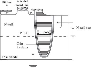
FIGURE 2.8
Schematic of the SPT cell cross section. (Redrawn from “A Substrate-Plate Trench-Capacitor (SPT) Memory Cell for Dynamic RAM’s”, N.C.C. Lu et al., IEEE. J.S.S Circuits, Vol. SC-21, pp. 627–633, Oct. 1986.)
For the SPT cell, an important design effort is to minimize the access device sub-threshold leakage in the well without compromising performance. This has been achieved in a 65 ns 4 Mbit DRAM with a cell area of 10.5 μm2 with 0.8 μm design rules [27]. In another realization using the SPT cell with its storage capacitor merged into the transistor isolation area, this area could be shrunk to 4 μm2 at 0.5 μm design rule and 16 Mbit chips were made available.
The SPT cell contains a vertical parasitic p+ (access transistor drain) n (n-well) p+ (substrate) FET along the trench wall, gated by the node polysilicon as shown in Figure 2.9, which is not present in the other trench cells. As gate and source are connected together, this parasitic device should remain in the limit of weak inversion, making it safe. In addition, making depletion region narrower is also attempted by using moderately doped retrograde n-well implant, making it safer. Although parasitic, the FET has its usefulness as it provides effective isolation between access transistor source region and the substrate, which can be used to further reduce the cell size by butting the source region to the trench wall. The leakage is thus smaller, because the n-well can either reject or sink carriers to reduce the disturbance to the storage node [28].
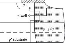
FIGURE 2.9
Parasitic FET device along the SPT cell trench sidewalls. (Redrawn from “A Substrate-Plate Trench-Capacitor (SPT) Memory Cell for Dynamic RAM’s”, N.C.C. Lu et al., IEEE. J.S.S Circuits, Vol. SC-21, pp. 627–633, Oct. 1986.)
If the SPT cell is not located within a well like first generation and other inverted trench cells, some extra design efforts would be needed. It is normal and essential in DRAMs to apply an array back-gate bias to reduce minority-carrier injection into the array [29]; however, if this back-gate bias is generated on chip, its application would generate considerable noise [30]. If the substrate is used both as the array bulk and the capacitor plate, this noise would be coupled directly to the storage node, and noise margin would be considerably reduced [26,30], whereas in the SPT cell located within a well the p+ substrate is connected to the low-noise ground and the n-well serves as the bulk array to which the generated back gate bias is applied.
In some advanced cell designs of this type, both the plate and storage electrode are fabricated inside the trench opening, which allows both electrodes to be completely oxide isolated. This provides the cell with punch-through protection even if the cells are placed very close to each other and reduces the soft-error rates relative to other inverted trench cells. A few of these are described below in brief.
2.3.2.2 Dielectrically Encapsulated Trench Cell
Capacitor structure of a dielectrically encapsulated trench (DIET) cell realized for a 16 Mbit DRAM is shown in Figure 2.10. The storage capacitor is formed with a poly-to-poly structure in the trench, and an insulator layer surrounds it to provide isolation between cells. As a result, it claims to have potential for achieving extremely small distance between cells with the advancement of fabrication process. The storage electrode formed in a trench cell is surrounded by a cell plate and storage electrode adjoins only a small depletion layer around the source/drain region of MOSFET. Such a structure leads to immunity from punch-through and drastically lowers the soft error rate compared to that for conventional trench capacitor cell. Doped impurities within the cell plate are prevented from diffusing out during the heat cycle in fabrication because the dielectric layer covers the cell plate. Without this, a depletion layer shall be present in series with the storage capacitor and its value shall be reduced. The cell plate bias voltage is fed from the substrate through a hole opened at the bottom of the dielectric capsule. This structure allows the cell to be made small, but there is a drawback that it is difficult to work with half-VDD biasing of the cell plate. Realization of a 16 Mbit DIET cell required a capacitor size of 0.87 μm x 1.6 μm with a depth of 4.0 μm that provided a capacitance of 28 fF with 25 nm thick oxide [31].
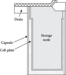
FIGURE 2.10
Schematic cross section of a DIET cell capacitor. (Redrawn from “Dielectrically Encapsulated Trench Capacitor Cell”, M. Taguchi et al., IEDM, pp. 136–138, 1986.)
2.3.2.3 Half-Vcc Sheath-Plate Capacitor Cell
The half-Vcc sheath-plate capacitor (HSPC) cell employs an inner storage node and half-Vcc plate operation through the use of buried plate-wiring which controlled capacitor plate voltage. The inner storage node has the advantage of low inter-trench current leakage and good immunity against injection of minority carriers due to cosmic irradiation. The half-Vcc plate operation allows the capacitance to be doubled and a negative substrate voltage to be used. Due to its highly self-aligned cell structure, it occupies only a small cell area of 4.2 μm2 (1.3 μm × 3.2 μm) for a 16 Mbit DRAM, in 0.6 μm technology, in which Si3N4-SiO2 composite film of 5.5 nm equivalent thickness was used to get 51 fF capacitance. The sheath plate is formed inside SiO2 sheath and is connected to the buried plate-wiring at the bottom of the groove. The word line is isolated from the storage node by the SiO2 layer, which is fabricated by using a self-aligned oxidation technique [32].
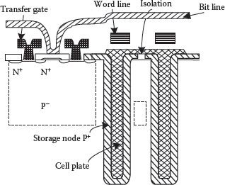
FIGURE 2.11
Schematic drawing of a DSP cell. (Redrawn from “Double Stacked Capacitor with self-aligned poly source/drain transistor (DSP) cell for megabit DRAM”, K. Tsukamoto et al., Proc. IEDM, pp. 328–331, 1987.)
2.3.2.4 Double Stacked Capacitor with Self-Aligned Poly Drain/Source Transistor Cell
A schematic diagram of a double stacked capacitor with self-aligned poly drain/source transistor (DSP) cell is shown in Figure 2.11. The storage capacitance, which is a combination of two capacitors, (1) between first polysilicon and substrate, and (2) between first and second polysilicon, which are stacked in a trench, results in a larger capacitance. The access transistor has a self-aligned poly source/drain, where the source/drain region is formed by a dopant diffusion into the substrate from the first polysilicon. Using unique self-aligned structure, 0.7 μm technology results in a cell of 5.92 μm2. With a trench depth of 4 μm, a storage capacitance over 50 fF could be obtained [33].
2.4 Access Transistor Stacked above Trench Capacitor Cell
In trench cell designs, access transistor is placed beside the trench and occupies a significant area of the cell, similar to planar access transistor cell where the capacitor was occupying a large part of the cell area. A more efficient use of cell area is achieved in a key development with transistor being stacked above the trench capacitor to form a vertical cell. It was first tried in VMOS DRAM cell [9] but could not succeed in manufacturability due to technological/processing problems in realizing sharply edged v-grooves with good oxide integrity. However, advances in process technology made it possible to realize three-dimensional buried trench cell for 64 Mbit and higher densities. Examples of such cell are described now.
2.4.1 Trench Transistor with Self-Aligned Contact Cell
The trench transistor with self-aligned contact (TSAC) cell has been developed for 4 Mbit and beyond density level, using following technologies: (1) a shallow trench forming the channel of the access transistor, as formation of such a transistor channel is for the improvement of short and narrow channel effects, and (2) bit line contact is formed with self-alignment to the word line; hence, the name TSAC. In the structure, marginless contact design capability enables substantial reduction of the memory cell size. In fact, TSAC revived efforts toward the formation of trench transistor cell which were terminated after the experience of VMOS discussed earlier [34].
The concept of storing signal charge on the poly was heavily attempted between 1984 and 1986. One of such configurations is the trench transistor cell (TTC) given by W.F. Richardson and others and soon used by A.H. Shah and others [35,36]. Both implemented TTCs were in 4 Mbit chips with cell areas of 10.6 μm2 in 0.8 μm technology and 9 μm2 in 1.0 μm technology, respectively. The TTC realizes a vertical transistor and capacitor in a deep trench. Earlier most of the cell designs focused on decreasing the planar area of the capacitor and/or optimizing the configuration of the capacitor to the access device. This occurred because well-researched and practiced planar technology gave excellent results when used in the fabrication processing of the devices and components. However, it became obvious to DRAM researchers that further scaling down of the cell area was not possible and change from planar to vertical device was unavoidable [37].
A schematic diagram of a trench transistor cell is shown in Figure 2.12. An 8 μm deep trench (1.3 μm × 1.5 μm) is etched in a 4.5 μm p-type epitaxial layer on a p+ substrate. A vertical access transistor is made in the top 2 μms whereas the storage capacitor is below the transistor in the trench. The inner plate of the capacitor is an n+ polysilicon plug, and the outer plate is the p+ substrate. The source of the transistor is connected to the n+ polysilicon plug of the capacitor by a buried lateral contact which is made by oxide undercut etch and refilled with polysilicon [35]. The drain, gate, and source of the trench pass transistor are made of diffused-buried n+ bit line, n+ polysilicon word line, and a buried lateral contact, respectively. The gate oxide thickness and channel length are around 25 nm and 1.5 μm, respectively, while the transistor width is determined by the perimeter of the trench.
FIGURE 2.12
Trench transistor cell schematic cross-section. (Redrawn from “Advanced cell structures for dynamic RAMs”, N.C.C. Lu, IEEE Circuits and Devices Magazine, pp. 27–36, Jan. 1989.)
The early DRAMs employing TTC used the open bit line architecture for the array, however the signal-to-noise ratio deteriorated with higher level of integration. The double ended adaptive folded (DEAF) bit line architecture has been used to obtain a 4 Mbit DRAM, which is in the form of a truly cross-point cell array [36]. The DEAF architecture has all the advantages of the conventional folded bit line scheme, and at the same time realizes a very dense cross-point memory cell array [38].
Characteristics of the access transistor in the TTC cell as well as the properties of the charge storage element have been studied in detail. Banerjee and others [39,40] reported the characteristics of the vertical trench transistor like that of reference [35] which was characteristically different from a planar transistor. Simulation of the trench transistor shows good agreement (within 10%) in both the linear and the saturation regions, but the threshold of the transistor is controlled by deep boron implant, having a nonuniform Gaussian profile. It indicates good sub-threshold slope, which allows low sub-threshold leakage, and statistical data from a large number of transistors indicate good uniformity of device characteristics and parameters.
In the earlier versions of TTCs, there were certain limitations. The trench sidewalls got oval cross section after patterning and reactive ion etching (RET), which resulted in different crystallographic orientation and hence gave different oxide thicknesses. The cell stored charge on the poly inside the trench, which was not located within a well and, therefore, could suffer substrate-plate bump effect if a substrate bias generator was used [40]. It was also observed that though thickness of thermal oxide dielectric was nonuniform around the oval trench perimeter, the oxide quality and leakage were comparable to planar oxide, and the capacitance was sensitive to the trench edge angle and depth [41]. Both the TSAC and TTC cells suffer high mask count due to using vertical devices in the array but having planar devices in peripheral circuits [36].
It is well known that thermally grown oxide becomes thinner both at top and bottom corners of trenches. It was extremely difficult to control precisely the growth of thin thermal oxide film without impurity redistribution using conventional furnace at high temperature. However, by using rapid thermal oxidation (RTO) process, highly reliable thin gate oxide can be grown reproducibly to realize the high performance megabit class DRAMs [42].
2.6 Buried Storage Electrode Cell
Buried storage electrode (BSE) cell is another example of an inverted trench cell in which storage electrode is inside a trench [43,44]. Basic structure of the BSE cell is shown in Figure 2.13(a), where a buried polysilicon electrode stores the signal charge. The storage node polysilicon refilled into the capacitor trench is connected to the access transistor electrode. The heavily doped substrate of a p/p++ epi wafer serves as the capacitor plate [43]. Most of the portion of the capacitor trench is deeply penetrated into the p++ substrate. Because of the use of heavily doped substrate, depletion layer at the capacitor surface is very thin, and hence inversion layer would not form. The cell is inherently free of punch-through between neighboring trenches and immune to soft errors. Due to its better immunity to soft errors, smaller storage capacitor is allowable. In a test cell in 0.8 μm design rules, an 8.8 μm2 cell realized 35 fF capacitance. With 0.8 μm trench isolation between capacitor trenches show negligible interference between adjacent cells, which is a major advantage at 4-MBit level in comparison to the first generation trench cells [13]. BSE cells and internal constant voltage (VBLS) convertor combined with half bit line voltage precharge, and high signal-to-noise ratio sensing, a 4 Mbit DRAM have been obtained [44]. Figure 2.13(b) shows a top layout view of BSE cells with folded aluminum bit line structure. The cell size is 2.3 μm × 4.6 μm with a 50 fF storage capacitance using 5 μm deep trenches. In 4 Mbit DRAM design using BSE cells the bit line driving high voltage must be limited to prevent the characteristic degradation of 1 μm gate cell transistors on account of hot carrier effects and to suppress voltage bounce of the cell capacitor electrode substrate. A suitable internal voltage converter could easily solve the problem.
FIGURE 2.13
(a) Schematic cross-section of a BSE cell. (b) Layout of a BSE cell. (Both figures redrawn from“Buried Storage Electrode (BSE) Cell for Megabit DRAMs”, M. Sakamoto. et al., Proc. IEDM, pp. 710–713, 1985.)
Because of the work-function difference between the p++ substrate and the n+ poly used in BSE cell capacitor, a higher voltage is dropped across its insulator compared to p+ poly in the SPT cell. The problem of voltage drop across the insulator is enhanced when a boosted word line is used or a substrate bias is used for the BSE cell. The constraint limits the scalability of the insulator thickness; otherwise the dielectric might break down. In addition, since along the trench sidewall in the cell there is a gated diode structure, leakage can become a serious concern, especially when the storage node voltage is high [45].
2.7 Buried Capacitor or Stacked Transistor Cell
Vertical access transistor has been used at 4–16 Mbit density DRAM level, like trench transistor cell [35], to reduce the cell area. However, the vertical transistor fabrication processes could not match the advantage of self-aligned planar technology, like better device uniformity, shallow junctions, shallow threshold implant adjustment, lightly doped drains, etc., which result in high performance. Alternatively a few cells have been designed in which capacitor is buried under the access device or the access transistor is stacked over the capacitor. Examples of stacked cell included a silicon-on-insulator (SOI) substrate-plate trench-capacitor (SS-SPT) cell [46] and a stacked switching transistor in SOI (SSS) cell [47]. The cells could be realized in a small area, as well as with very low SER and leakage on account of having SiO2 as the substrate for the planar transistor; however, its quality depended on the technology advancements in SOI technology. Obtaining SOI films of fine quality for submicron devices was difficult in the 1980s. In addition, a floating-substrate transistor has different characteristics in comparison to the bulk planar transistor.
Development of a self-aligned epitaxy-over-trench (SEOT) technology in a submicron CMOS process has realized a three-dimensional buried trench (BT) cell having a potential for high-density DRAMs. The technology allowed a bulk horizontal access transistor formed on top of the trench transistor with self-aligned vertical via connection to the buried capacitor. Hence, the BT cell showed a high performance transistor and small size, with possibility of realizing DRAM of 64 Mbit densities and beyond [48].
Figure 2.14 shows the schematic view of the BT cell in which the trench storage capacitor is accessed through the horizontal transistor, and it is completely isolated from the heavily doped substrate, which serves as grounded plate. The bulk horizontal transistor is fabricated in an epitaxial layer over the BT capacitor. The self-aligned vertical via connection between access transistor and top of the buried capacitor is known as neck. A single-crystal p-type silicon layer is grown over the p++ substrate till it completely surrounds and reaches the top level of the trench capacitor. A self-aligned window is formed on the top of the trench and the oxide on top of the trench is etched; neck is formed on top of the exposed polysilicon in the trench, and then a second epi film is grown. A flat surface results after a certain minimum amount of epitaxial growth, followed by isolation, and a MOS transistor is fabricated.
FIGURE 2.14
Schematic of a BT cell, showing possible parasitic backside leakage path as well. (Redrawn from “A Buried-Trench DRAM Cell Using a Self-Aligned Epitaxy over Trench Technology”, N.C.C. Lu et al., IEDM Tech. Dig., pp. 588–590, 1988.)
Operation of the cell is similar to that of a conventional SPT cell [49]. However, the BT cell suffers from a minimal backside leakage path between the storage node and the bit line node, i.e., between the source and the drain of the access transistor gated by the node polysilicon inside the trench as shown in Figure 2.14. The possible leakage depends on the n-well doping level and its bias, oxide capacitor thickness tcap, epitaxial film thickness tnec and the trench extension from the source edge text. Simulated results have shown that the backside leakage component can be made negligible [48].
In planar MOS capacitor cells, signal charges were considerably reduced in the inversion and depletion layers due to the influence of the minority carriers generated in silicon substrate. Koyanagi tried to eliminate the inversion capacitance and the depletion capacitance by employing a different passive capacitance known as metal insulator metal structure as a storage capacitor in a three-dimensional (3-D) cell in 1978 and named it stacked capacitor cell (STC). Figure 2.15 shows the basic structure of a stacked capacitor cell where the storage capacitor is three dimensionally stacked on a switching transistor [50]. Self-aligned contact is used to connect the bottom electrode of the capacitor to the source/drain region, and to connect the bit line to source/drain of the switching transistor. By using the stacking, not only was the area occupied by the capacitor reduced, but the use of high dielectric material as capacitor insulator also became practically feasible. First Si3N4 was used instead of SiO2 as capacitor insulator and polycrystalline silicon for the two electrodes to increase the storage capacitance and then Ta2O5 film, having dielectric constant five to six times that of SiO2 was employed [51]. A discussion on MIS/MIM capacitors is included in Chapter 5.
FIGURE 2.15
Basic structure of stacked capacitor cell (STC). (“The Stacked Capacitor DRAM Cell and Three Dimensional Memory”, M. Koyanagi et al., IEEE SSCS News, pp. 37–41, Winter 2008.)
Memory cells with three-dimensional capacitors such as stacked capacitor cells [52] were realized for obtaining sufficient storage capacitance at still higher memory density levels. Starting from the basic idea of the STC cell, further progress was made; cylindrical capacitor [53] and double stacked capacitor [54] are typical examples, and shall be studied later. Another significant advantage of stacked capacitor was that the signal charges stored in the MIS/MIM capacitor were not affected by the carriers generated in the substrate. This means that the structure is considerably less affected by soft errors.
The trendsetter stacked capacitor [52] had some limitations as well. It required the connection of bit-line to the access transistor’s drain through the window in the plate electrode. If alignment tolerance limit between the plate and the bit line contact hole is taken into consideration, the storage node pattern design results in the decrease of storage capacitance. The limitation was overcome by forming stacked capacitor structure by a number of studies in the 1980s at the DRAM level of 4 Kbit to 64 Kbit. Koyanagi and others [55] gave three similar stacked capacitor cell structures with slight difference in the position of the stacked capacitor as shown in Figure 2.16. In Figure 2.16(a) the storage capacitor had a poly-Si,-Si3N4-Al layer stacked on the access transistor, bit line and field oxide; in Figure 2.16(b), the storage capacitor as a poly-Si-Si3N4-poly-Si structure is stacked on the access transistor and field oxide, and in Figure 2.16(c) capacitor is stacked on the field oxide only. Stacked capacitor of Figure 2.16(c) was used for the realization of 16 Kbit memory because of better compatibility with the conventional fabrication process. Another stacked capacitor cell was realized by forming storage capacitor on bit line using a diagonal active stacked-capacitor with a high-packed storage node (DASH) for use in a 16 Mbit DRAM [56]. In this scheme active area is set diagonal to both the word line and bit line. Figure 2.17 shows some process steps of the DASH. After word line formation, the polycide bit line is formed directly on the word line. When SiO2 sidewall is formed, the storage node contact area is automatically opened. No precise patterning is needed; the bit lines are covered by the storage node and the plate electrode. Storage capacitance of 35 fF/bit was obtained in a cell size of 3.4 μm2 using 0.5 μm design rule with 5 nm thin composite dielectric film of SiO2 and Si3N4. Similar attempt was made by using double layered storage node structure with slightly modified fabrication procedure of exchanging the order to open contact window and to deposit poly-Si of the lower electrode to get sufficient cell capacitance in 16 Mbit DRAMs [57].
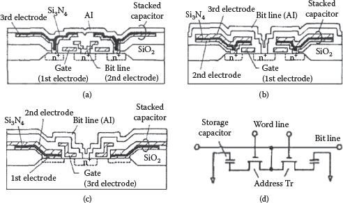
FIGURE 2.16
Cross-sectional configuration of three types of STC cells. (a) Top capacitor type, (b) intermediate capacitor type, (c) bottom capacitor type, and (d) its equivalent circuit. (“A 5-V Only 16-kbit Stacked-Capacitor MOS RAM”, M. Koyangi et al., IEEE. Journal of Solid State Circuits, Vol. SC-15, No. 4, 1980.)
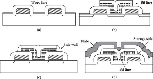
FIGURE 2.17
Process flow of the DASH. (a) Transfer gate formation, (b) bit line formation, (c) bit line isolation by sidewall SiO2, and (d) capacitor formation by storage node and plate. (“A New Stacked Capacitor DRAM Cell Characterized by a Storage Capacitor on a Bit-Line Structure”, S. Kimura et al., Proc. IEDM, pp. 596–599, 1988.)
Realizing capacitor over bit lines (COB) changed the memory cell structure and the fabrication steps considerably. These capacitor-over-bit line (COB) cells were found to have immunity to inter-bit-line noise as the bit lines were shielded by the storage electrode. Structure has shown potential for realizing gigabit DRAM by introducing high dielectric constant capacitor film [58]. Earlier COB structures [59,60] required complex active area pattern to form the capacitor contact due to which DRAM in gigabit density could not be produced commercially. However, in a straight-line-trench isolation and trench-gate transistor (SLIT) simple straight line layout of the active area is formed [62]. In addition, isolation width and the gate length are also reduced to less than design rule using the sidewall-aided fine pattern etching (SAFE) technique.
With Pt/Ta as capacitor electrode, (BaxSr1-x) TiO3 film was used for the first time to realize a 256 Mbit DRAM in COB structure [58]. A 100 nm thick dielectric film was equivalent to 8 Å of SiO2. Combination of COB and high dielectric constant material in MIM capacitors then progressed fast. Stacked capacitor cell was employed in a 1 Mbit DRAM production for the first time by Fujitsu, with a cell area of 26.46 μm2 with having 55 fF capacitance [62]. Increase in the cell capacitance from 35 fF to 55 fF was possible by utilizing the curvature and sidewall of second layer poly-Si as shown in Figure 2.18. First layer polycide forms the word line and the second layer poly-Si, which is extended over its own word line and the next word line forms the storage node. Cell capacitor is formed between the second and third layer poly-Si, which forms the cell plate.
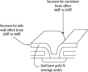
FIGURE 2.18
Increase of cell capacitance using three dimensions, a projected area of 10.0 um2 realizing a 35 fF capacitance. (Redrawn from “A 1Mb DRAM with 3-Dimensional Stacked Capacitor Cells”, Y. Takemae et al., IEEE. Int. Solid State Circuit Conference, pp. 250–251, 1985.)
Hitachi produced a 4 Mbit, 1-Mbit × 4 DRAM using a stacked capacitor cell in 1987 using a twisted driveline sense amplifier (TDSA) scheme and the multiphase drive circuit (MPD) on a 0.8 μm double-well CMOS technology [63]. In the TDSA scheme two drive lines of the CMOS amplifiers cross each other in the middle of the array, which reduces the total capacitance associated with each drive line to half of its value. The MPD circuit for PMOS drives reduces peak charging current of bit lines and maintains at nearly constant value. Combination of TDSA and MPD helped in obtaining the access time of 65 ns.
Further scaling of stacked capacitor cell (STC) from 4 Mbit level to 64 Mbit was hardly able to satisfy both the cell area and storage capacitance requirement because dielectric films with less than 3 nm SiO2-equivalent thickness was required at 64 Mbit DRAM. To overcome this limitation one of the methods applied was to use poly-Si film with rugged surface of electrode; that is, morphology of the poly-Si storage electrode decides increase in effective surface area/capacitance realized. A second alternative was to use more than one layer of storage electrode and/or by using both sides of the electrode, surrounded by thin dielectric and top capacitor plate; effective capacitance was to be increased without increasing the projected area. Polysilicon storage electrodes, which are called membranes or fins, can expand horizontally, vertically, or in both directions. It was found that 0.1 μm poly-Si film deposited at 570°C had 2.5 times larger rugged surface area than the film deposited at conventional temperature of 620°C, giving larger capacitance [64].
2.8.1 Horizontal and Vertical Fin Structured Capacitor Cells
Examples of the horizontal fin structures include double stacked [54, 60], and spread stacked [65]. The storage node completely overlaps the storage contact in the double stacked horizontal fin structure; however, it also needed two additional masking steps. Since 16 Mbit DRAMs were not feasible with single fin stacked capacitors, a curved storage electrode was used by Takemae and others [62]. It is observed that sidewall storage effect on capacitance realized is more significant, but thick storage polysilicon makes further processing difficult. To overcome this problem a new cell architecture in which bit lines are formed before storage electrode is realized [60]. A comparison of the cell architecture with a conventional cell for comparison is shown in Figure 2.19. It is observed that large capacitor in this fin type capacitor cell is obtained as bit line contact hole is not needed. In addition, bit line coupling can be reduced because the cell plate acts as a shield. Another significant example of horizontal fin structure is spread stacked capacitor (SSC) cell with its schematic cross section shown in Figure 2.20 [65]. As shown in Figure 2.20, storage electrode of a memory cell is expanded to the neighboring memory cell area, so each storage electrode occupies two memory cell areas, enhancing the storage capacitance to 1.8 times that of a conventional cell. Table 2.1 shows the advantage of the storage capacitance of the SSC cell over the conventional STC cell. For 64 Mbit DRAMs, cell size must be less than 1.3 μm2 with minimum feature size of 0.3 μm and a 4 nm SiO2-equivalent dielectric film. The SSC cell can achieve satisfactory value of 27 fF whereas conventional STC cell capacitance is less than 15 fF.
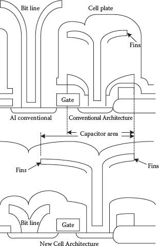
FIGURE 2.19
Comparison of conventional and new cell architecture in which bit lines are formed before storage electrode. (Redrawn from “3-Dimensional Stacked Capacitor Cell For 16M And 64M DRAMs”, T. Ema et al., IEDM Tech. Dig., pp. 592–595, 1988.)
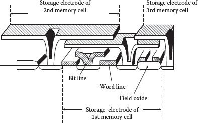
FIGURE 2.20
Schematic cross-section of the spread stacked capacitor cell. (Redrawn from “A Spread Stacked Capacitor (SSC) cell for 64 Mb DRAMs” S. Inone et al., in Proc., IEDM, p. 31, 1989.)
Comparison of Storage Capacitance Realized in Conventional STC Cell and SSC Cell
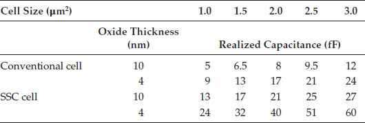
Figure 2.21 shows the schematic cross-section view of a dual cell plate (DCP) cell [66] used in a 64 Mbit DRAM. To increase the storage capacitance, dual cell plates completely surround the whole surface of the storage poly-Si. Using 0.5 μm lithography, a fabricated cell needs 2.88 μm2 chip area and realizes 50 fF capacitance with 5 nm thin dielectric and 600 nm thick storage poly-Si. The DCP cell has a potential to realize more than 25 fF in 1.3 μm2 cell area when 0.3 μm design rule is used. The DCP cell may be considered as one of the variations of the fin-type stacked cell.
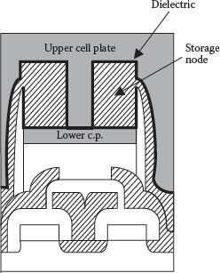
FIGURE 2.21
Schematic cross-sectional view of a DCP CELL. (Redrawn from “A Spread Stacked Capacitor (SSC) cell for 64 Mb DRAMs” S. Inone et al., in Proc., IEDM, p. 31, 1989.)
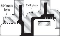
FIGURE 2.22
Simplified view of a cylindrical cell. (Adapted from “Novel Stacked Cell for 64 Mb DRAM”, W. Wakamiyia et al., Symp. VLSI Techn., Dig. Tech. Papers, p. 31, 1989.)
Vertical fin structure cells at initial phase of development are now discussed briefly. In 1989, Wakamiya and others [53] gave the cylindrical storage node cell. Figure 2.22 shows cylindrical storage node cell in simplified form used by Mitsubishi [67]. About 0.5 μm high cylinder realizes 25 fF capacitance using 1.5 μm2 cell area, with a condition that the shielded bit line electrode is combined with the cylindrical capacitor. The cell is realized in fully self-aligned manner and fabrication process is simple. Another advantage of the cell is that difference of steps between memory cell area and peripherals circuits are reduced, improving interconnections. Another bit line shielded stacked capacitor cell with storage capacitor formed over bit line cylindrical storage node structure is realized by Kawamoto and others in 1990 [59]. The cylindrical storage node is formed using polymide sacrificial layer and poly-Si using CVD on it. In addition, planarized bit line wiring reduces the bit line resistance making high-speed operation possible. The planarized bit line along with cylindrical storage node is shown in cross-section form in Figure 2.23.
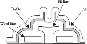
FIGURE 2.23
Cylindrical storage node using polymide reverse pattern and poly-Si CVD. (Adapted from “A 1.28 μm2 Bit-Line Shielded Memory Cell Technology for 64 Mb DRAMs”, Y. Kawamoto et al., VLSI Symp. Tech. Digest, pp. 13–14, 1990.)
A self-aligned crown-shaped stacked capacitor cell has been developed by T. Kaga and others [68], using 0.3 μm electron-beam lithography having a cell area of 1.28 μm2. A large effective capacitance area of 3.7 μm2 and a Ta2O5 film equivalent to a 2.8 nm SiO2 film ensures a large capacitance charge of 33 fC, which is equivalent to storage capacitance of 44 fF at 1.5 V (Vcc/2) operation. Layout of the CROWN cell is an improved version of the DASH cell [69]. Larger plane area could be created without any alignment problems because storage capacitors are formed on the openings among the data lines and the word lined after these lines are formed. Figure 2.24 shows the cross section of the CROWN cell.
A double cylindrical storage spread-vertical capacitor (SVC) cell has been given for 64 Mbit and 256 Mbit DRAM [70,71]. As shown in Figure 2.25, an exploded view of SVC illustrates that storage capacitor spreads to the neighboring cell area. Each storage electrode A′ and B′ of the two adjacent memory cells (A, B) is connected through a poly-Si via to the memory cells A and B, respectively. The storage electrodes A′ and B′ form the inner wall loop and the outer wall loop, respectively. Structure of SVC provides a simple fabrication and 24 fF capacitance for 256 Mbit DRAM with only 0.4 μm capacitor height. Since storage capacitance is proportional to the peripheral length of the foot prints of the capacitor including two adjacent memory cells, it becomes three times that of the conventional stacked capacitor (STC).
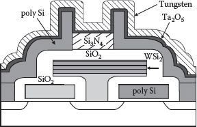
FIGURE 2.24
Schematic view of a CROWN cell. (Redrawn from “Crown-Shaped Stacked-Capacitor Cell for 1.5V Operation 64-Mb DRAMs”, T. Kaga et al., IEEE Trans. Electron. Devices, Vol. 38, No. 2, pp. 255–260, 1991.)
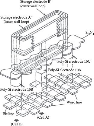
FIGURE 2.25
An exploded view of the spread vertical capacitor cell. (“Spreaded Vertical Capacitor Cell (SVC) for beyond 64 MBit DRAMs”, N. Matsuo et al., IEDM, pp. 473–476, 1991.)
1. V. Leo Rideout, “One-Device Cells for Dynamic Random-Access Memories: A Tutorial,” IEEE Trans. Electron Devices, Vol. ED-26, no. 6, pp. 839–852, June 1979.
2. K.U. Stein and H. Friedrick, “A 1-mil2 Single Transistor Memory Cell in Silicon-Gate Technology,” IEEE J. Solid State Circuits, Vol. SC-8, pp. 319–323, Oct. 1973.
3. V. Leo Rideout, “Double Polysilicon Dynamic Memory Cell with Polysilicon Bit Line,” IBM Tech. Disc. Bull., Vol. 21, pp. 3828–3831, Feb. 1979.
4. Y.A. El-Mansy and R.A. Burghard, “Design Parameters of the Hi-C DRAM Cell,” IEEE. J.S.S. Circuits, Vol. SC-17, pp. 951–956, 1982.
5. C.G. Sodini and T.I. Kamins, “Enhanced Capacitor for One Transistor Memory Cell,” IEEE Trans. Electron Devi., Vol. ED-23, p. 1187, 1976.
6. A. Tasch et al., “The Hi-C RAM Cell Concept,” Trans. Electron Devi., Vol. ED-25, p. 33, 1978.
7. R.H. Dennard et al., “Design of Ion Implanted MOSFETs with Very Small Physical Dimensions,” IEEE J.Solid State Circuits, Vol. SC-9, pp. 256–268, Oct. 1974.
8. F.B. Jenne, U.S. Patent 4,003,036, 1977.
9. J.J. Barnes, S.N. Shabde, and F.B. Jenne, “The Buried Source VMOS Dynamic RAM Device,” Electron Devices Meeting, (10.1109/IEDM.1977.189135) Vol. 23, pp. 272–275, Dec. 5–7, 1977.
10. P. Chaterji et al., “Trench and Compact Structures for DRAM’s,” Proc. IEDM, pp. 128–131, 1986.
11. H. Sunami et al., “A Corrugated Capacitor Cell (CCC) for Megabit Dynamic MOS Memories,” IEEE IEDM Technical Digest, pp. 806–808, Dec. 1982.
12. T. Mano et al., “Submicron VLSI Memory Circuits,” IEEE ISSCC Tech. Digest, pp. 234–235, Feb. 1983.
13. H. Sunami et al., “Scaling Consideration and Dielectric Breakdown Improvement of Corrugated Capacitor Cell (CCC) for Future DRAM,” IEDM Dig. Tech. Papers, pp. 232–235, 1984.
14. T. Furuyama et al., “An Experimental 4Mb CMOS DRAM,” ISSCC Dig. Tech. Papers, pp. 272–273, 1986; also IEEE J.Solid State Circuits, Vol. 21, pp. 605–611, Oct. 1986.
15. T. Sumi et al., “A 60 ns 4Mb DRAM in a 300 mil DIP,” ISSCC Dig. Tech. Papers, pp. 282–283, 1987.
16. M. Wada, K. Heida, and S. Watanabe, “A Folded Capacitor Cell (FCC) for Future Megabit DRAMs,” Proc. of IEDM, pp. 244–247, 1984.
17. T. Furuyama and J. Frey, “A Vertical Capacitor Cell for ULSI DRAMs,” Symp. on VLSI Tech. Dig. Tech. Papers, pp. 16–17, 1984.
18. S. Nakajima et al., “An Isolation Merged Vertical Capacitor Cell for Large Capacity DRAMs,” IEDM Dig. Tech. Papers, pp. 240–243, 1984.
19. T. Mano et al., “Circuit Technologies for 16 Mb DRAMs,” ISSCC Dig. Tech. Papers, pp. 22–23, 1987.
20. H. Kotani et al., “A 4 Mb DRAM Design Including 16-Bit Concurrent ECC,” Symp. on VLSI Circuits Dig. Tech. Papers, pp. 87–88, 1987.
21. K. Nakamura et al., “Buried Isolation Capacitor (BIC) Cell for Megabit MOS Dynamic RAM,” IEEE IEDM Tech. Digest, pp. 236–239, Dec. 1984.
22. M. Nagamoto et al., “A High Density 4M DRAM Process Using Folded Bitline Adaptive Sidewall Isolated Capacitor (FASIC) Cell,” IEDM Tech. Dig., pp. 144–147, 1986.
23. K. Mashiko, “A 90 ns 4Mb DRAM in a 300 mil DIP,” IEEE International Solid-State Circuits Conference, pp. 312–315, 1987.
24. P. Bakeman et al., “A High Performance 16-Mb DRAM Technology,” Symp. on VLSI Technology, pp. 11–12, 1990.
25. N.C.C. Lu et al., “A Substrate-Plate Trench-Capacitor (SPT) Memory Cell for Dynamic RAM’s,” IEEE J.S.S Circuits, Vol. SC-21, pp. 627–633, Oct. 1986.
26. N.C.C. Lu, H.H. Chao, and W. Hwang, “Plate Noise Analysis of an On-Chip Generated Half-VDD Biased Plate PMOS Cell in CMOS DRAMs,” IEEE J. Solid-state Circuits, Vol. SC-20, no. 6, pp. 1272–1276, 1985.
27. R. Parent et al., “A 4 Mb DRAM with Double-Buffer Static Column Architecture,” ISSCC Dig. Tech. Papers, pp. 14–15, 1987.
28. W. Noble et al., “Parasitic Leakage in DRAM Trench Storage Capacitor Vertical Gated Diode,” IEDM Dig. Tech. Papers, pp. 340–343, 1987.
29. H. Masuda et al., “A 5V Only 64K Dynamic RAM Based on High S/N Design,” IEEE J.Solid State Circuits, Vol. 15, pp. 846–854, Oct. 1980.
30. M. Takada et al., “A 4 Mb DRAM with Half Internal Voltage Bitline Precharge,” ISSCC Dig. Tech. Papers, pp. 270–271, 1986.
31. M. Taguchi et al., “Dielectrically Encapsulated Trench Capacitor Cell,” IEDM, pp. 136–138, 1986.
32. T. Kaga et al. “A 4.2 μm2 Half-VCC Sheath Plate Capacitor DRAM Cell with Self-Aligned Buried Plate-Wiring,” IEDM, pp. 332–335, 1987.
33. K. Tsukamoto et al., “Double Stacked Capacitor with Self-Aligned Poly Source/Drain Transistor (DSP) Cell for Megabit DRAM,” Proc. IEDM, pp. 328–331, 1987.
34. M. Yanagisawa, K. Nakamurs, and M. Kikuchi, “Trench Transistor Cell with Self-Aligned Contact (TSAC) For Megabit MOS DRAM,” IEDM Dig. Tech. Papers, pp. 132–135, 1986.
35. W.F. Richardson et al., “A Trench Transistor Cross Point DRAM Cell,” Proc. IEDM, pp. 714–717, 1985.
36. A.H. Shah et al., “A 4 Mbit DRAM with Trench Transistor Cell,” IEEE J.Solid-State Circuits, Vol. 20, pp. 618–626, Oct. 1986.
37. N.C.C. Lu, “Advanced Cell Structures for Dynamic RAMs,” IEEE Circuits and Devices Magazine, pp. 27–36, Jan. 1989.
38. A.H. Shah et al., “A 4 Mb DRAM with Cross-Point Trench Transistor Cell,” IEEE Int. Solid-State Circuits Conf., pp. 267–268, 1986.
39. S.K. Banerjee et al., “Characterization of Trench Transistors for 3-D Memories,” VLSI Tech. Symp. pp. 79–80, May, 1986.
40. S. Banerjee, et al., “Leakage Mechanism in the Trench Transistor DRAM cell,” Trans. Electr. Dev., Vol. ED-35, pp. 108–116, 1988.
41. K. Rao et al., “Trench Capacitor Design Issues in VLSI DRAM Cells,” IEDM Dig. Tech. Papers, pp. 140–143, 1986.
42. K. Yoneda et al., “Trench Capacitor Using RTO for Megabit DRAMs,” VLSI Techn. Dig. Tech. Papers, pp. 95–96, 1987.
43. M. Sakamoto et al., “Buried Storage Electrode (BSE) Cell for Megabit DRAMs,” Proc. IEDM, pp. 710–713, 1985.
44. M. Takada et al., “A 4 Mb DRAM with Half Internal Voltage Bitline Precharge,” IEEE Int. S.S.C. Conf., pp. 270–271, 1986.
45. S. Banerjee et al., “A Band-to-Band Tunneling Effect in the Trench Transistor Cell,” Symp. VLSI Tech., Dig. Tech. Papers, pp. 97–98, 1987.
46. N.C.C. Lu, “Three Dimensional Dynamic RAM Cell,” U.S. Patent 620,667, 1984.
47. M. Ohkura et al., “A Three Dimensional DRAM Cell of Stacked Switching Transistor in SOI (SSS),” IEDM Dig. Tech. Papers, pp. 718–721, 1985.
48. N.C.C. Lu et al., “A Buried-Trench DRAM Cell Using a Self-Aligned Epitaxy Over Trench Technology,” IEDM Tech. Dig., pp. 588–590, 1988.
49. N.C.C. Lu et al., “The SPT Cell—A New Substrate-Plate Trench Cell for DRAMs,” IEDM Dig. Tech. Papers, pp. 771–772, 1985.
50. M. Koyanagi et al., “The Stacked Capacitor DRAM Cell and Three Dimensional Memory,” IEEE SSCS News, pp. 37–41, Winter 2008.
51. M. Koyanagi et al., “Novel High Density, Stacked Capacitor MOS RAM,” Extended Abs. 10th Conf. Solid State Devices, 1978.
52. M. Koyanagi et al., “Novel High Density, Stacked Capacitor MOS RAM,” IEDM Tech. Dig., pp. 348–351, Dec. 1978.
53. W. Wakamiyia et al., “Novel Stacked Cell for 64 Mb DRAM,” Symp. VLSI Techno., Dig. Tech. Papers, p. 31, 1989.
54. T. Kisu et al., “Novel Storage Capacitance Enlargement Structure Using a Double Stacked Storage Node in STC DRAM Cell,” SSDM Ext. Abs., p. 581, 1988.
55. M. Koyangi et al., “A 5-V Only 16-kbit Stacked-Capacitor MOS RAM,” IEEE Journal of Solid State Circuits, Vol. SC-15, pp. 661–666, 1980.
56. S. Kimura et al., “A New Stacked Capacitor DRAM Cell Characterized by a Storage Capacitor on a Bit-Line Structure,” Proc. IEDM, pp. 596–599, 1988.
57. H. Watanable, K. Kurosawa, and S. Sawada, “Stacked Capacitor Cell for High-Density Dynamic RAMs,” Proc. IEDM, pp. 600–603, 1988.
58. K. Koyama et al., “A Stacked Capacitor with (BaxSr1-x) TiO3 for 256M DRAM,” IEDM. Tech. Dig., pp. 823, 1991.
59. Y. Kawamoto et al., “A 1.28 μm2 Bit-Line Shielded Memory Cell Technology for 64 Mb DRAMs,” VLSI Symp. Tech. Digest, pp. 13–14, 1990.
60. T. Ema et al., “3-Dimensional Stacked Capacitor Cell for 16M and 64M DRAMs,” IEDM Tech. Dig., pp. 592–595, 1988.
61. M. Sakao et al., “A Straight-Line-Trench Isolation and Trench-Gate Transistor (SLIT) Cell for Giga-bit DRAMs,” IEEE Symp. VLSI Tech., 1993.
62. Y. Takemae et al., “A 1Mb DRAM with 3-Dimensional Stacked Capacitor Cells,” IEEE Int. Solid State Circuit Conference, pp. 250–251, 1985.
63. K. Kimura et al., “A 65-ns 4 Mbit CMOS DRAM with a Twisted Driveline Sense Amplifier,” IEEE J. of Solid State Circuits, Vol. SC-22, no. 5, Oct. 1987.
64. M. Yoshimura et al., “Rugged Surface Poly-Si Electrode and Low Temperature Deposited Si3N4 for 64 MBit and Beyond STC DRAM Cell,” Proc. IEDM, pp. 659–662, 1990.
65. S. Inone et al., “A Spread Stacked Capacitor (SSC) Cell for 64 Mb DRAMs,” Proc. IEDM, p. 31, 1989.
66. H. Arima et al., “A Novel Stacked Capacitor Cell with Dual Cell Plate for 64 Mb DRAMs,” Proc. IEDM, pp. 651–652, 1990.
67. T. Matsukawa and T. Nakano, “Stacked Capacitor Cells for 64 Mb DRAM,” VLSI Tech. Systems and Appl., pp. 264–267, 1991.
68. T. Kaga et al., “Crown-Shaped Stacked-Capacitor Cell for 1.5V Operation 64-Mb DRAMs,” IEEE Trans. Electron. Devices, Vol. 38, no. 2, pp. 255–260, 1991.
69. S. Kimura et al., “A Diagonal Active-Area Stacked Capacitor DRAM Cell with Storage Capacitor on Bitline,” IEEE Trans. Electron Devices, Vol. 37, pp. 737–743, 1990.
70. N. Matsuo et al., “Spreaded-Vertical-Capacitor Cell (SVC) for beyond 64 MBit DRAMs,” IEDM, pp. 473–476, 1991.
71. N. Matsuo et al., “Spread-Vertical-Capacitor Cell (SVC) for High-Density DRAM’s,” IEEE Trans. Electron Devices, Vol. 40, no. 4, pp. 750–753, 1993.