
Chapter 10. Creating Custom Components
The more you work with Arduino devices in general, and the AVR microcontroller in particular, the more you may come to realize just how flexible and versatile they are. There seems to be a sensor or shield for almost any application you might imagine, and new shields appear on a regular basis. Even so, there are still a few applications for which there is no shield. There may be times when you spend hours online searching fruitlessly for a shield with specific capabilities, only to finally realize that it just doesn’t exist. In that situation you basically have three choices: first, you could just give up and try to find another way to solve the problem; second, you might find someone to build it for you (for a fee, usually); or third, you could design and build your own PCB. This chapter describes two projects that illustrate the steps involved in creating a custom shield and an Arduino software–compatible device.
The first project is a shield, shown in Figure 10-1, that is intended for a specific range of applications. The GreenShield, as I’m calling it, is based on a conventional shield form factor. It utilizes surface-mount components in a layout that includes potentiometers, relays, and LEDs.
When coupled with an Arduino the GreenShield will be able to function as a stand-alone monitor and controller for gardening or agricultural applications. This shield can also serve as the foundation for an automated weather station, a storm warning monitor, or a thermostat (note that a programmable thermostat built using ready-made modules and sensors is described in Chapter 12).
The second half of this chapter describes the Switchinator, an AVR ATmega328-based device that doesn’t rely on the Arduino bootloader firmware, but can still be programmed with the Arduino IDE and an ICSP programming device. The Switchinator PCB is shown in Figure 10-2.
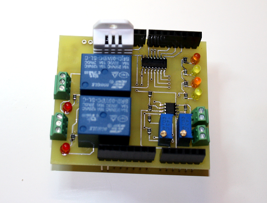
Figure 10-1. The GreenShield
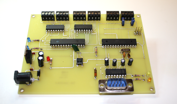
Figure 10-2. The Switchinator
The Switchinator can remotely control up to 14 DC devices such as relays or high-current LEDs, drive up to 3 unipolar stepper motors, or control AC loads using external solid-state relays. It uses an RS-232 interface and does not require a connection to a host PC via USB.
The Switchinator incorporates all of the essential components of an Arduino into a board of our own design. We won’t need to worry about the socket header dimensions and layout considerations required for a shield PCB; the only constraints on overall size and shape will be those that we impose on the design.
With some patience and a plan you can easily create a custom PCB that doesn’t look anything like an Arduino, but has the same ease of programming. Best of all, it will do exactly what you design it to do, and in a physical form that exactly meets your requirements.
Creating a PCB is not all that difficult, but it is a task that requires some knowledge of PCB design and electronics. There are low-cost/no-cost software tools available to handle PCB layout chores, and getting a circuit board fabricated is actually rather easy. The projects in this chapter will also require some soldering skill, particularly in the case of surface-mounted components. If you’re already experienced in these areas, then you’re almost there. If not, then learning how to create a schematic, work with PCBs, use a soldering iron, and select the right parts can be an enjoyable and rewarding experience.
For the shield PCB we will use the Eagle schematic capture and PCB layout tool, and for the Arduino-compatible PCB we’ll use the Fritzing tool. Both of these are very common and capable tools. Best of all, they are free (well, Fritzing is free, and the entry-level version of Eagle, with limitations, is available at no cost).
Note
When creating custom shields or Arduino-compatible boards, you can do yourself a huge favor by keeping a notebook. Even if it’s nothing more than a collection of printed or photocopied pages in a three-ring binder, you will be grateful if you need to look up some tidbit of information in the future for a similar project. Why not just save it all on disk in your PC? Because it can evaporate if the disk drive fails without a backup, or even get lost in the crowd if there are lots of things already stored on the drive (this happens to me more than I’d like to admit). Also, putting it into a notebook allows you to go back later and annotate things as you gain experience with testing, fabricating, and deploying your device. Red pens aren’t just for high school English teachers.
This chapter also provides a list of resources for software, parts, and PCB fabrication. The only assumption I’ve made is that you may already have some electronics experience, or at least be willing to put in a little extra effort to learn some of the basics. Be sure to take a look at the brief overview of tools in Appendix A, and definitely check out the reading suggestions found in Appendix D. Finally, don’t forget to peruse articles from websites like Hackaday, Makezine, Adafruit, SparkFun, and Instructables. You can also find tutorial videos on YouTube. Many others have been down these paths before, and many of them have been kind enough to document their adventures for the benefit of others.
Note
Remember that since the main emphasis of this book is on the Ardunio hardware and related modules, sensors, and components, the software shown is intended only to highlight key points, not present complete ready-to-run examples. The full software listings for the examples and projects can be found on GitHub.
Getting Started
As with any endeavor worth devoting any significant amount of time to, planning is essential. This applies to electronics projects just as it applies to the development and implementation of complex software, building a house, designing a Formula 1 race car, or mounting an expedition to the Arctic. As the old saying goes, “Failure to plan is planning to fail.”
Every project that is beyond trivial can be broken into a series of steps. In general, there are seven basic steps to creating an electronic device:
-
Define
-
Plan
-
Design
-
Prototype
-
Test
-
Fabricate
-
Acceptance test
Some projects may have fewer steps and some more, depending on what is being built. Here’s some more detail about each step:
- Define
-
In formal engineering terms this might be referred to as the requirements definition phase, or, more correctly, the functional requirements definition phase. A brief description of what the end result of the project will do and how it will be used is sufficient for simple things. A more detailed description will probably be needed for something complex, like a shield for use with an Arduino on board a CubeSat. But regardless of the complexity, putting it down in writing can help chart the course for the steps to come, and it can also reveal omissions or errors that may otherwise go unnoticed until it’s too late to easily make substantive changes. Lastly, it’s a good idea to write the project definition such that it can be used to test a prototype or a finished device. If the functional requirements don’t clearly state what the device is supposed to do in such a way that someone could use this description to test the device, then it really isn’t a good set of requirements and it doesn’t define the desired device or system very well.
Writing functional requirements may sound like the equivalent of watching paint dry, but it’s actually an essential aspect of engineering. If you don’t know where you are going, how can you tell when you get there? A good requirement, of any type, should have four basic characteristics: (1) it should be consistent with itself and the overall design, (2) it should be coherent so that it makes sense, (3) it should be concise and not overly wordy, and (4) it must be verifiable. A functional requirement that states that “The device must be able to heat 100 milliliters of water in a 250 ml beaker to 100 degrees C in 5 minutes” is testable, but a statement like “The device must be able to make hot water” is not (How hot? How long? How much water?).
- Plan
-
Sometimes planning and definition can happen in the same step, if the device is something relatively simple and well understood. But in any case, the planning step involves identifying the information necessary for the design step and getting as much essential information assembled in one place as possible—things like component datasheets, parts sources, identification of necessary design and software tools, and so on. The idea is to go into the design step with everything needed to make good decisions about what is available, how long it may take to get it, and how it will be used.
The planning step is also where you make some educated guesses as to how long it will take to complete each of the upcoming steps: designing, prototyping, testing, fabrication, and acceptance testing. I say “educated guesses” here because you should have some idea of what will be involved after collecting as much information as possible, but these are guesses because no one has a crystal ball that can let them see the future. Unexpected things can happen, and sometimes it takes longer to complete some aspect of the project than could be realistically anticipated. This is just how things go in the real world. It’s also why people who do project management for a living multiply their time estimates by a factor of two or three. It’s better to overestimate and get it done early than to underestimate the amount of time necessary and deliver it late.
A planning tool is handy both for establishing a realistic schedule and as a way to gauge progress. My favorite tool for quick and simple scheduling is the timeline chart, also known as a Gantt chart in fancier form. These can be complicated affairs created using project management software, or simple charts like the one shown in Figure 10-3.
For many small projects the fancy charts are not necessary, and the added complexity is just extra work. The important things are: (1) all the necessary tasks are accounted for in the planning, (2) the plan is realistic from both time and resource perspectives, and (3) the plan has a definite objective and ending. One other thing to notice about the simple timeline chart is that some tasks start before a preceding task is complete, and the chart does not show the dependencies that would indicate a critical path. I have found that for small projects involving one or just a few people, this overlapped scheduling more realistically reflects how things really happen.
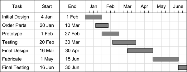
Figure 10-3. Example timeline chart
- Design
-
For a hardware project, the design step is where the circuit diagrams start to emerge and the design of the physical form takes shape. With the project definition and the planning information in hand, what needs to be done should be clear. While defining the circuitry is what most people think of when considering design, other significant activities in the design step include selecting components for form and fit, evaluating electrical ratings of components and environmental considerations (humidity, vibration, and temperature), and perhaps even potential RFI (radio frequency interference) issues.
When designing a new device there are always choices to be made. Sometimes the reason for choosing one method over another comes down to cost and availability of parts or materials. The intended functionality is another consideration, such as in the case where an input control may need to perform more than one function. Other times the choice might be based on aesthetics, particularly if there is no cost benefit of going one way over another. Lastly, in some cases it’s just a matter of using something that is known and familiar rather than working with something unknown. This isn’t always the best reason for making a choice, but it does happen quite often.
Regardless of the type of project (hardware, software, structure, or whatever), the design step is typically iterative. It’s not realistic to expect that the design will just fall into place on the first attempt, unless perhaps it’s something profoundly trivial (and even then, it’s not a sure thing). Actually, design and prototyping (discussed next) work together to identify potential problems, devise feasible solutions, and refine the design. This is common in engineering, and while sometimes aggravating, iteration is an essential part of design refinement.
- Prototype
-
For simple things, such as a basic I/O shield with no active circuitry, building a prototype may not really be necessary (or even feasible). In other cases, a prototype can be used to verify the design and ensure that it performs according to the definition created at the start of the project. For example, it might not be a good idea to jump right into laying out a PCB for a device that combines an AVR processor, an LCD display, a Bluetooth transceiver, a multiaxis accelerometer, and an electronic compass, all on the same PCB. It might all work the first time, but if there are unforeseen subtle issues, they may not be apparent until after the PCB has already been made and paid for. Building and testing a prototype first can save a lot of aggravation and money later.
Problems identified with a prototype feed back into the design to help improve it. In an extreme case the prototype might even demonstrate that the initial design is just wrong, and you might need to start over. While this is annoying, it’s not a disaster (it’s actually more common than you might think). Building a hundred circuit boards only to find out that there is a fundamental design flaw—now that’s a disaster. Prototyping, testing, and design revision can prevent that from occurring.
- Test
-
The essence of testing is simply, “Does it correctly do what it’s supposed to do, and does it do it as safely and reliably as intended?” The project definition created at the outset is the yardstick used to determine if the device has the desired functionality and exhibits the required safety and reliability. This is basic functional testing. It can get a lot more complicated, but unless you plan to send your design into space (or to the bottom of the ocean), or it will be controlling something that could cost a lot of money if something goes wrong (or damage something else, such as human beings), then basic functional testing should be sufficient for the prototype.
A word about the differences between “correct,” “safe,” and “reliable”: just because something behaves in a correct way doesn’t means it’s safe (safe can also mean “operates without introducing unacceptable risk”), and something that behaves in a safe way isn’t necessarily correct or even reliable. If a device won’t turn on, it could be considered to be safe and reliable (it reliably will not do anything), but it definitely would not be correct. Lastly, to say that something is correct and reliable does not automatically mean that it’s safe. A power tool such as a handheld circular saw may correctly and reliably cut lumber, but it will also correctly and reliably cut off a hand just as easily. An electrical device with an internal short circuit will reliably emit smoke (and perhaps even some flames) when power is applied, but the overall operation is neither safe nor correct.
- Fabricate
-
After the prototype has been tested and has demonstrated correct behavior in accordance with the functional requirements, the design can move on to the fabrication stage. This step may involve fabricating a PCB and then loading it with parts. It might also refer to the integration of prefabricated modules and associated cables and wires into an enclosure or a larger system. In terms of possible delays, fabrication can be problematic. A supplier might be out of stock of a critical component, or if the assembly has been contracted, the assembly house might be having some problems or be overbooked. Custom-made parts might be late for any number of reasons.
Fortunately, if you are only making one or a few of something and you are doing all of the fabrication yourself, then you can avoid many of these potential problems. It still doesn’t hurt to give yourself plenty of time, however. Making a run to the hardware store for a box of 3/8 inch 6-32 machine screws takes time, and if they’re out of stock then it is going to take that much longer to try another store. Of course, if the planning and design steps were done with an eye toward what would be needed for fabrication, then you should have all the components, PCBs, nuts, bolts, screws, washers, connectors, wire, brackets, and glue you will need.
- Acceptance test
-
This last step is also known as final testing, since it is the last thing to occur before the device is deemed ready to use or deploy. Some basic functional testing was already done with the prototype, but now it is time to test the final product. This is definitely not duplicated effort. It’s all too easy to mount the wrong part on a PCB, or even install a part backward. Also, circuits on a PCB will sometimes behave differently than those built on a solderless prototyping block, so thoroughly testing the assembled device is always a good idea.
The testing is typically conducted in two steps. The first step verifies that the device or system behaves in the same manner as the prototype. The idea is to apply the same tests used with the prototype to verify that nothing has changed. In software engineering this is referred to as regression testing. The next step of testing involves additional tests to verify that the thing you’ve built works correctly in its final configuration with actual I/O. This is why this step is referred to as acceptance testing, and the main point is to answer the question, “Is the device or subsystem acceptable for its intended application?”
Custom Shields
There are basically three primary form factors to consider when designing an Arduino shield. These are the baseline, extended, and Mega pin layouts. The original or baseline (a.k.a. R2) layout, found on the Duemilanove, Uno R2, and other older boards, can be considered to be the standard for shield layouts, but that doesn’t mean a shield can’t be designed to utilize the extended (a.k.a. R3) layout found on later-model Uno and Leonardo boards. Shields can also been designed to utilize all of the pins on a Mega-style Arduino, and there’s no reason why a shield has to have the same outline shape as an Arduino. Some shields, such as those with relays or large heat sinks, have a physical form factor suited to the components on the shield, rather than the Arduinos to which they are connected.
A novel approach that ignores size constraints is to create a large PCB with a set of pins arranged so that an Arduino can be connected in an inverted position. This might sound odd, but take a look at Figure 10-4. This is a board from a Roland SRM-20 desktop CNC milling machine. You can read more about it at Nadya Peek’s infosyncratic.nl blog.
Figure 10-4. An inverted Arduino on a large PCB (image courtesy of Nadya Peek)
If you are designing a shield to sell commercially, then you may want to use the baseline layout as your template, since it will also work just fine with an Uno or Leonardo board, as well as a Mega-type PCB. Chapter 4 describes each of these board types and provides dimensions and pinout information.
The small form-factor Arduino boards such as the Nano, Mini, and Micro are unique in that they have all of the I/O pins on the bottom of the PCB, rather like a large IC. Adding a shield to one of these boards entails using an adapter, like the one shown in Figure 10-5, to bring out the signals to pin sockets for connecting a shield PCB.
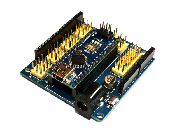
Figure 10-5. Arduino Nano interface adapter PCB
You might notice in Figure 10-5 that pin socket headers have been added to the PCB. This was done largely as an experiment to see what would be involved in physically interfacing a Nano with a regular shield. With some creativity one could conceivably plug a shield into the board, except for the fact that the Nano sits too high on its socket headers. One solution would be to use extensions for the shield pins, which are just extended pin socket headers with some of the pin length removed. A more drastic solution would be to desolder the existing headers for the Nano and replace them with shorter types. I recommend the pin extension option. This chapter doesn’t cover the steps involved in creating this type of adapter.
Using something like a Nano, Mini, or Micro Arduino with a shield actually doesn’t make a whole lot of sense most of the time (although in Chapter 12 there is an example where this was done for a particular application). It does make sense to treat these small PCBs as if they were large ICs, and use them as components on a large PCB.
Physical Considerations
Be aware that on the Duemilanove PCB, and probably other boards as well, there are two surface-mounted capacitors that can collide with the extra pins found on the power and analog connector row of some shields designed for the R3 extended baseline layout. Some variants of the Uno also have components that can collide with shield pins.
Another consideration is that the type B USB jack found on the Duemilanove and Uno boards can potentially short out against a shield PCB. The DC power jack on these boards can also interfere with a shield PCB. Although it is plastic and won’t short anything, it can prevent the shield from seating completely. Figure 10-6 shows this situation with a Duemilanove and an Ethernet shield.
For these reasons, it’s a good idea to either size the length of the shield so that it won’t interfere with the underlying Arduino, or design the component placement on the shield PCB to leave collision areas blank. See the next section, Chapter 4, and Chapter 8 for more on PCB dimensions and shield stacking.
When designing a shield you may also want to consider what will no longer be accessible on the Arduino under the shield and what can, or cannot, be mounted on it. This includes the reset button, the surface-mounted LEDs, and the ICSP pin group. Some shields deal with this by simply replicating the pinout of the Arduino board. Others, like most LCD shields, may not replicate the Arduino’s pins to the top side of the shield PCB, but sometimes provide a reset button. With an LCD shield this makes sense, of course, since it would be the top shield in a stack in any case.
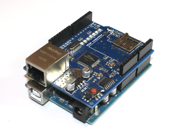
Figure 10-6. Duemilanove with shield
Stacking Shields
One of the nice things about the Arduino form factor is the ability to stack shields. You could create a stack containing a base Arduino board (an Uno, for example) with an SD memory card shield on top of it, followed by an input/output shield of some sort, and then an LCD or TFT display shield on top of all of that. Presto, you now have a basic data logging device.
What can be mounted above a shield should always be a consideration, be it another shield or perhaps some type of sensor module. When selecting components for a shield it is wise to consider the height of the various parts. If the parts are too high and another shield cannot be physically attached without interfering with something, then that shield will always need to be on the top of the stack.
There are basically two ways to allow for shield stacking: staggered socket and pin headers, and extended pin socket headers. Staggered, in this context, means that the upper connectors (socket headers) are offset from the lower pins (pin headers) by some amount, with both the upper digital I/O and power/analog headers shifted to the same side by the same amount.
In Figure 10-7 you can see a modular I/O shield on a Duemilanove. There are a few things to notice here. First, the modular I/O shield uses the staggered connector approach, so it is not vertically edge-aligned with the underlying Arduino board. This may need to be taken into account if the assembly will be mounted in some type of enclosure that might be subjected to shock or vibration—it may not be possible to secure the shield with nuts and bolts. Secondly, the shield does not bring out the ICSP pins, so that functionality is effectively lost (which may, or may not, be a big deal). Lastly, the pins of the connectors along the edge of the shield above the Arduino’s power and USB connector can (and do) collide, so some type of insulating shim is necessary.
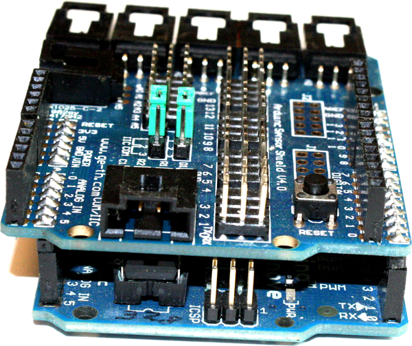
Figure 10-7. Example of a staggered shield
Extended pin connector sockets are a common variation on the 0.1 center connectors that have a long pin that goes through the PCB. The pin is long enough to make a solid connection with an underlying board, and the connector sockets provide for another shield board to mount on top and be in alignment with the shield below it. These are found on many shields, and you should look for them when selecting a shield.
A big consideration in shield design is Arduino pin usage. This is in addition to stacking concerns. The pins used by a shield determine what else can be used with that shield in a stack. Avoiding exclusive use of the SPI and I2C pins means other shields can be used in a stack, including SD and microSD flash memory, I/O expander, Bluetooth, ZigBee, Ethernet, and GSM shields. In other words, don’t repurpose the SPI or I2C pins unless the shield design absolutely needs them.
Sometimes you may encounter shields that someone obviously thought were a good idea, but which don’t always work out so well in practice. I/O shields often have multiple blocks of connector pins that are rendered inaccessible if another shield is placed on them. Other shields have solder pads that interfere with the ICSP pins on the Arduino PCB. Problems like these are not uncommon. Unfortunately it’s not always possible to know in advance if there are problems with a shield, and sometimes the only way to know if a particular shield might have physical mounting issues is to purchase one and try it.
Electrical Considerations
If your custom shield has nothing but passive components (i.e., connectors, switches, resistors), power supply requirements probably won’t be an issue for the board. However, if it has LEDs or active circuitry, it is a good idea to consider how much power it will need, and where it will get it. Even something as simple as an LED draws some power, and enough of them can overload an AVR processor and do some damage.
As a general rule, if a shield has one or more relays or connectors to attach things that could draw more than a few milliamps each, then some type of driver circuit or IC should be considered. It is possible to operate a shield from a separate power supply, but passing signals between the Arduino and the shield can sometimes be tricky.
If a shield has its own DC power source, then ground might also be something to consider. There are three ground sockets on a baseline Arduino: two on the side with the analog inputs and one on the digital I/O side. If you use only one of the Arduino’s ground sockets for the signal ground reference for a shield, you can avoid potential problems with induced noise and ground loops. Although these situations are very rare, they are still a possibility, particularly for shields that may incorporate high-gain operational amplifiers or high-frequency circuits. Applying good design practices can help avoid strange and hard-to-diagnose problems in the future.
The GreenShield Custom Shield
In this section we will create a custom shield to illustrate the steps involved in the design and fabrication of an Arduino shield. The shield will be a humidity, temperature, ambient light, and soil moisture monitor. It is intended mainly for use in a greenhouse, although with the correct enclosure, some solar cells, and a wireless transceiver of some sort it could be put into a field to monitor the turnips (or whatever). As water gets scarcer in some parts of the world (including the Western United States), keeping an eye on the soil moisture content as well as temperature and humidity can help to minimize watering times and volumes while still keeping the crops healthy. The farmer can sit in the living room and get a quick readout of how things are doing in the field from a smartphone, tablet, or desktop PC.
I’m calling this the GreenShield, for obvious reasons, and the definition and planning steps are combined into one step. The GreenShield is physically very simple, and the main hardware design challenge will be fitting some large components (two relays and a DHT22) onto a small shield PCB.
Objectives
The goal of this project is to create a shield that can be used as an autonomous remote monitor to sense temperature, humidity, soil moisture content, and ambient light level. Based on predefined sensor input limits, it will control two relays.
The relays can be used to control a water valve, and perhaps a fan or maybe some lights to compensate for cloudy days. It also has six LEDs: two for high and low humidity points, two for high and low soil moisture levels, and an LED for each relay to indicate activity.
The software will support a command-response protocol and maintain an internal table of automatic relay functions mapped to sensor inputs and limits. Alternatively, a host control computer can obtain the sensor readings on demand and control the relays directly.
Definition and Planning
The shield will incorporate a DHT22 combination temperature and humidity sensor, a light-dependent resistor (LDR) sensor (see Chapter 9) to detect the ambient light level, and a conductivity-based soil moisture probe. Two relays will provide automatic or commanded control of external devices or circuits.
Sensor inputs:
-
Temperature
-
Relative humidity
-
Soil moisture (relative)
-
Ambient light level
Control and status outputs:
-
Two control relays, software function definable, 10A control capability
-
Four LEDs to indicate soil moisture and humidity limits
-
Two LEDs to indicate relay status
Electrical interface:
-
Two-position terminal block for moisture probe input
-
Two-position terminal block for LDR connection
-
One three-position terminal block per relay (NC, C, and NO)
-
+5V DC supplied by attached Arduino board
Control interface:
-
Command-response protocol, control host driven
-
Sensor readings available on demand
-
Relay override by control host
All of the components will be placed on a standard baseline-type shield, with dimensions as described in Chapter 4. Most of the components will be surface-mount types, with the exception of the terminal blocks, the relays, and the DHT22 temperature and humidity sensor.
Design
The GreenShield is intended to be used without a display or user controls. In other words, it and an Arduino will operate as an autonomous remote sensor and controller. It can be connected to another computer system (the master host system) to receive operating parameters, return sensor data, and override relay operation.
Autonomous in this case means the GreenShield will be able to operate the relays automatically when specific conditions are met, such as humidity, soil moisture, or light levels. The software will accept commands from a master computer to set the various threshold levels and override the operation of the relays. It will generate a response on command containing the current temperature, humidity, light level, and relay states. All interactions between the control host and a GreenShield Arduino will be command-response transactions.
The GreenShield software will be developed entirely with the Arduino IDE. The host computer used to compile and upload the finished code will also serve as the test terminal interface when the code is running on the Arduino. Ideally one would want to create a custom interface program using something like Python, or, in a Windows environment, a terminal emulator like TeraTerm. It includes an excellent scripting facility, and I highly recommend it.
Functionality
The first consideration is the physical design of the shield PCB. The block diagram shown in Figure 10-8 gives an overview of what types of functions will be on the shield.
Note that in Figure 10-8 none of the hardware functions interact directly. The sensors, LEDs, and relays are just extensions of the Arduino’s basic I/O capabilities.
The humidity/temperature sensor is mounted on the PCB, while the photocell (a light-dependent resistor) and the soil moisture probe can be located off-board if desired. Miniature terminal blocks are used for sensor connections, so no soldering or connector crimping is required.
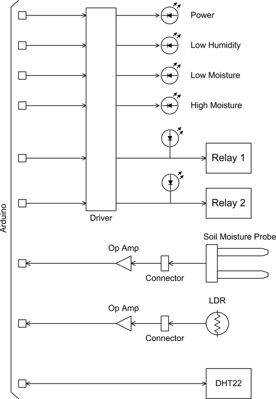
Figure 10-8. GreenShield block diagram
The GreenShield is intended to be the last (top) shield on a stack. This is due to the relays and the temperature/humidity sensor, all of which are tall enough to prohibit stacking another shield.
Hardware
Circuit-wise the GreenShield isn’t very complicated, as can be seen in the schematic shown in Figure 10-9. A ULN2003A is used to drive status LEDs and two relays. A dual op amp is used to buffer the voltage level from a soil moisture sensor and an LDR for input to the AVR ADC.
The sensors connected to the op amp inputs are effectively variable resistors, and with the two trimmer potentiometers they form a voltage divider. The trimmers can be adjusted to achieve an optimal response from the op amp without driving it too far one way or the other voltage-wise.
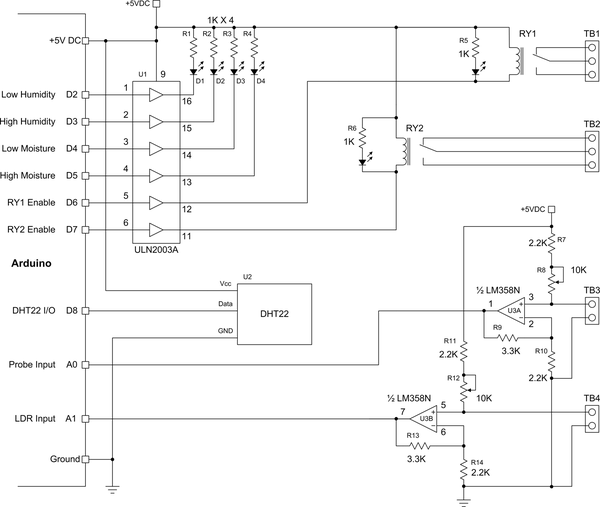
Figure 10-9. GreenShield schematic
The GreenShield has been designed to allow for extending the Arduino shield stack by avoiding critical digital and analog I/O pins. Table 10-1 lists the Arduino pins and assignments used for the GreenShield.
| Pin | Function | Pin | Function |
|---|---|---|---|
D2 |
ULN2003A channel 1 |
D7 |
ULN2003A channel 6 |
D3 |
ULN2003A channel 2 |
D8 |
DHT22 data input |
D4 |
ULN2003A channel 3 |
A0 |
Soil moisture sensor input |
D5 |
ULN2003A channel 4 |
A1 |
LDR sensor input |
Notice that the SPI pins—D10, D11, D12, and D13—are not used, so they are available for SPI shields. D0 and D1 are also available if you want to connect an RS-232 interface and forgo the USB. A4 and A5 are available for I2C applications.
Now that we have a schematic we can assemble a complete parts list, which is given in Table 10-2.
| Quantity | Type | Description | Quantity | Type | Description |
|---|---|---|---|---|---|
2 |
SRD-05VDC-SL-C |
Songle 5A relay |
4 |
2.2K ohm, 1/8W |
Resistor |
1 |
DHT22 |
Humidity/temperature sensor |
2 |
3.3K ohm, 1/8W |
Resistor |
1 |
Generic |
LDR sensor |
2 |
10K trim |
PCB mount potentiometer |
1 |
SainSmart |
Soil moisture probe |
2 |
0.1” (2.54 mm) |
3-position terminal block |
6 |
3 mm |
LED |
2 |
0.1” (2.54 mm) |
2-position terminal block |
1 |
LM358N |
Op amp |
2 |
0.1” (2.54 mm) |
8-position socket header |
1 |
ULN2003A |
Driver IC |
2 |
0.1” (2.54 mm) |
6-position socket header |
6 |
1K ohm, 1/8W |
Resistor |
1 |
Custom |
Shield PCB |
Software
The GreenShield software is based on three primary functions: sensor input, command parsing and output generation, and relay function mapping. The first function is responsible for obtaining data from each of the four sensor inputs (temperature, humidity, soil moisture, and ambient light level) and storing the values for use by other parts of the software. The command parsing functions interpret the incoming command strings from a host PC and generate responses using the command-response protocol described here. The output functions control the relays based on the sensor inputs and preset limits defined by the various commands.
The command-response protocol used for transactions between the host computer and the GreenShield Arduino is shown in Table 10-3. Note that the GreenShield only responds to the host; it will never initiate a transaction on its own.
You can use the built-in serial terminal tool in the Arduino IDE, or you can exit from the IDE and connect directly to the USB port that the Arduino with the GreenShield happens to be using. This approach can be used to create a user interface application for setting up the GreenShield and monitoring its operation. In practice the idea is to configure the GreenShield software on an Arduino and then let it run unattended.
- Status query commands
-
The GreenShield software provides four query commands. These are listed in Table 10-4. These commands allow a control host to get the current on/off state of either of the two relays, the last value read from either the LDR or the moisture sensor analog input, and the latest temperature and relative humidity reading from the DHT22 sensor.
Table 10-3. GreenShield command-response protocol (all commands) Command Response Description AN:n:?AN:n:valGet analog input
nin raw DNGT:HMXGT:HMX:valGet humidity max value
GT:HMNGT:HMN:valGet humidity min value
GT:LMXGT:LMX:valGet light max value
GT:LMNGT:LMN:valGet light min value
GT:MMXGT:MMX:valGet moisture max value
GT:MMNGT:MMN:valGet moisture min value
GT:TMXGT:TMX:valGet temp max value
GT:TMNGT:TMN:valGet temp min value
HM:?HM:valReturn current humidity
RY:n:?RY:n:nReturn status of relay
nRY:n:1OKSet relay
nONRY:n:0OKSet relay
nOFFRY:A:1OKSet all relays
ONRY:A:0OKSet all relays
OFFRY:n:HMXOKSet relay
ntoONif humidity >= maxRY:n:HMNOKSet relay
ntoONif humidity <= minRY:n:LMXOKSet relay
ntoONif light level >= maxRY:n:LMNOKSet relay
ntoONif light level <= minRY:n:MMXOKSet relay
ntoONif moisture >= maxRY:n:MMNOKSet relay
ntoONif moisture <= minRY:n:TMXOKSet relay
ntoONif temp >= maxRY:n:TMNOKSet relay
ntoONif temp <= minST:HMX:valOKSet humidity max value
ST:HMN:valOKSet humidity min value
ST:LMX:valOKSet light max value
ST:LMN:valOKSet light min value
ST:MMX:valOKSet moisture max value
ST:MMN:valOKSet moisture min value
ST:TMX:valOKSet temp max value
ST:TMN:valOKSet temp min value
TM:?TM:valReturn current temperature
Table 10-4. GreenShield query commands Command Response Description RY:n:?RS:n:nReturn status of relay
nAN:n:?AN:n:valGet analog input
nin raw DNTM:?TM:valReturn latest DHT22 temperature
HM:?HM:valReturn latest DHT22 humidity
- Relay override commands
-
The relays on the GreenShield may be controlled via software commands. Four relay control commands allow an individual relay to be set to either on or off, or both relays may be set on or off at one time. Table 10-5 lists the relay override commands.
Note
Note that when a relay is set using an override command any previous setpoint mapping is deleted. To use the relay again with a setpoint, one of the setpoint commands must be sent to the GreenShield.
Table 10-5. GreenShield relay commands Command Response Description RY:n:1OK
Set relay
nONRY:n:0OK
Set relay
nOFFRY:A:1OK
Set all relays
ONRY:A:0OK
Set all relays
OFF - Relay action mapping commands
-
The activation of either of the two relays may be mapped to a specific minimum or maximum setpoint condition for humidity, light level, soil moisture content, or ambient temperature. Table 10-6 lists the relay setpoint commands. When mapping an action to a relay, the most recent mapping command will override any previous command.
- Setpoint commands
-
The minimum and maximum setpoints are defined using the ST commands, listed in Table 10-7. The setpoint value may be returned to the host control PC using the GT commands. The setpoint values may be modified at any time.
The relay function mapping associates a relay with a sensor input and a set of state change conditions in the form of upper and lower limits. A relay may be enabled if a sensor value is above or below a limit set by the host control system. Relay association is not exclusive, meaning that both relays could be assigned to the same sensor input and limit conditions. This might not make sense to do, but it can still be done.
| Command | Response | Description |
|---|---|---|
|
|
Set relay |
|
|
Set relay |
|
|
Set relay |
|
|
Set relay |
|
|
Set relay |
|
|
Set relay |
|
|
Set relay |
|
|
Set relay |
| Command | Response | Description |
|---|---|---|
|
|
Set humidity max value |
|
|
Set humidity min value |
|
|
Set light max value |
|
|
Set light min value |
|
|
Set moisture max value |
|
|
Set moisture min value |
|
|
Set temp max value |
|
|
Set temp min value |
|
|
Get humidity max value |
|
|
Get humidity min value |
|
|
Get light max value |
|
|
Get light min value |
|
|
Get moisture max value |
|
|
Get moisture min value |
|
|
Get temp max value |
|
|
Get temp min value |
Although the GreenShield is currently configured for two relays, there is no hard limit on the number of relays that could be used. As can be seen from Table 10-1 the I2C pins (A4 and A5) are available, so an I2C digital I/O expander shield can be used to connect additional devices to the Arduino.
Prototype
To create the prototype for this project I’m using something called a Duinokit, which is shown in Figure 10-10. This clever thing has an array of sensors, LEDs, switches, and other accessories along with an Arduino Nano, all mounted on a large PCB with lots of socket headers. It also has a position for attaching a conventional shield (or stack of shields). It’s like a modern take on the old all-in-one electronics project kits that were once popular.
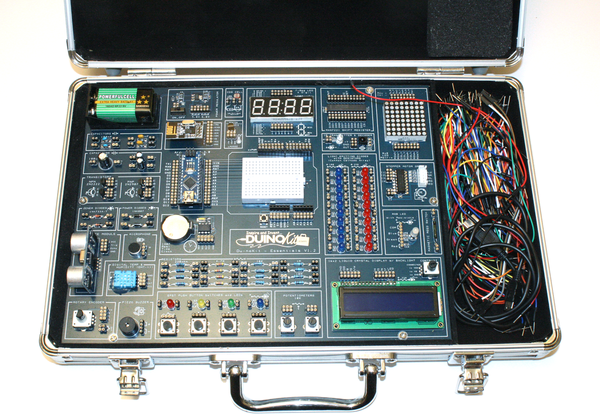
Figure 10-10. The Duinokit
An equally valid approach would be to assemble all the necessary components from a sensor kit and just about any Arduino, but the Duinokit keeps things neat and tidy, and it provides a nice development platform to use to create the software while waiting for the PCB and some of the other parts to show up. The Duinokit is available from http://duinokit.com and through Amazon.com.
The Duinokit has one DHT11 temperature/humidity sensor, which is a slower, lower-resolution version of the DHT22 that will be used with the GreenShield. In terms of software, the DHT11 and DHT22 are similar but not identical. The DHT22 uses a different data word (bit string) than the DHT11 to accommodate the improved accuracy of the DHT22 sensor.
The LDR and soil moisture sensor use an LM358 dual op amp, with one-half assigned to each input. I placed the LM358 on the solderless breadboard provided on the Duinokit’s single large PCB. This also provided a place to mount the resistors, and the two 10K potentiometers on the Duinokit served as the input offset trim controls.
Prototype software
The software will be developed in prototype and final forms. The first step is to create software to run on the Duinokit prototype that will read sensor inputs, verify that the LM358 op amp circuits are behaving as expected, and support some testing to determine initial input range limits. The next step is the development of the final software that will support the command-response protocol defined in “Software” and the relay function mapping. The actual shield hardware will be used to develop the final software.
The prototype software is intended for reading data from the analog inputs and the on-board DHT11 sensor. This is what will be used for prototype testing when the initial input ranges are established. The output appears in the serial monitor window provided by the Arduino IDE. The prototype test software shown in Example 10-1 is contained in a single sketch file called gs_proto.ino.
Tip
The functions shown in Example 10-1 for the various temperature conversions and dewpoint values aren’t really necessary for the basic Greenshield. I’ve included them as examples if you want to use them.
Example 10-1. GreenShield sensor prototype software
// GreenShield prototype software// 2015 J. M. Hughes//// Uses DHT11 library from George Hadjikyriacou, SimKard, and Rob Tillaart//// Repeatedly reads and outputs temperature, humidity, soil moisture,// and light level. No relay setpoint functionality.#include <dht11.h>// Definitions#define LHLED 2// D2 Low humidity LED#define HHLED 3// D3 High humidity LED#define LMLED 4// D4 Low moisture#define HMLED 5// D5 High moisture#define RY1OUT 6// D6 RY1 enabled#define RY2OUT 7// D7 RY2 enable#define DHT11PIN 8// D8 DHT11 data#define SMSINPUT A0// A0 SMS input#define LDRINPUT A1// A1 LDR input// Global Varsintcurr_temp=0;// current (latest) temperatureintcurr_hum=0;// current humidityintcurr_ambl=0;// current ambient light levelintcurr_sms=0;// current soil moistureintcntr=0;// dht11 object is globaldht11DHT11;// Read data from DHT11 and store in curr_hum and curr_temp global// variables for later usevoidreadDHT(){if(!DHT11.read(DHT11PIN)){curr_hum=DHT11.humidity;curr_temp=DHT11.temperature;}}// Read data from analog inputs via LM358 op amp circuits and store// in curr_ambl and curr_sms for later usevoidreadAnalog(){curr_ambl=analogRead(LDRINPUT);curr_sms=analogRead(SMSINPUT);}// Celsius to Fahrenheit conversion// From example code found at http://playground.arduino.cc/main/DHT11LibdoubleFahrenheit(doublecelsius){return1.8*celsius+32;}// Celsius to Kelvin conversion// From example code found at http://playground.arduino.cc/main/DHT11LibdoubleKelvin(doublecelsius){returncelsius+273.15;}// dewPoint() function NOAA// reference: http://wahiduddin.net/calc/density_algorithms.htm// From example code found at http://playground.arduino.cc/main/DHT11LibdoubledewPoint(doublecelsius,doublehumidity){doubleA0=373.15/(273.15+celsius);doubleSUM=-7.90298*(A0-1);SUM+=5.02808*log10(A0);SUM+=-1.3816e-7*(pow(10,(11.344*(1-1/A0)))-1);SUM+=8.1328e-3*(pow(10,(-3.49149*(A0-1)))-1);SUM+=log10(1013.246);doubleVP=pow(10,SUM-3)*humidity;doubleT=log(VP/0.61078);// temp varreturn(241.88*T)/(17.558-T);}// delta max = 0.6544 wrt dewPoint()// 5x faster than dewPoint()// reference: http://en.wikipedia.org/wiki/Dew_point// From example code found at http://playground.arduino.cc/main/DHT11LibdoubledewPointFast(doublecelsius,doublehumidity){doublea=17.271;doubleb=237.7;doubletemp=(a*celsius)/(b+celsius)+log(humidity/100);doubleTd=(b*temp)/(a-temp);returnTd;}voidsetup(){// Init the serial I/OSerial.begin(9600);// Set up the AVR's pinspinMode(LHLED,OUTPUT);pinMode(HHLED,OUTPUT);pinMode(LMLED,OUTPUT);pinMode(HMLED,OUTPUT);pinMode(RY1OUT,OUTPUT);pinMode(RY2OUT,OUTPUT);// Initial current data variablescurr_temp=0;curr_hum=0;curr_ambl=0;curr_sms=0;}voidloop(){// Get DHT11 readingsreadDHT();// Get LDR and SMS readingsreadAnalog();// Print data to outputSerial.println("");Serial.("Raw LDR : ");Serial.println(curr_ambl);Serial.("Raw SMS : ");Serial.println(curr_sms);Serial.("Humidity (%) : ");Serial.println((float)DHT11.humidity,2);Serial.("Temperature (oC) : ");Serial.println((float)DHT11.temperature,2);Serial.("Temperature (oF) : ");Serial.println(Fahrenheit(DHT11.temperature),2);Serial.("Temperature (K) : ");Serial.println(Kelvin(DHT11.temperature),2);Serial.("Dew Point (oC) : ");Serial.println(dewPoint(DHT11.temperature,DHT11.humidity));Serial.("Dew PointFast (oC): ");Serial.println(dewPointFast(DHT11.temperature,DHT11.humidity));// Scroll up to align displayfor(inti=0;i<12;i++)Serial.println();delay(1000);}
The setup() function simply initializes and opens the serial I/O, sets some pin modes, and
clears the global variables for current data readings. Each time the readDHT()
and readAnalog() functions are called they will obtain the latest
values from the DHT11 and the analog inputs and place them into these variables.
The main loop reads the analog inputs and the DHT11, formats the data, and writes the current values to the USB serial monitor. It does not communicate with a control host computer and it doesn’t do any relay setpoint mapping. Its purpose is to continuously obtain and display sensor data.
The prototype uses an open source library for the DHT11. The final version will use
a custom library for the DHT22, but it’s not needed for the prototype. The DHT11
library by George Hadjikyriacou, SimKard, and Rob Tillaart is available from
the Arduino Playground. The Fahrenheit(), Kelvin(), dewPoint(),
and dewPointFast() functions are from the same source.
Prototype testing
Using the Duinokit we can test the various sensor input functions of the GreenShield and fine-tune the operation. If there’s a problem with the circuitry (which will be easy to resolve, given that it’s so simple), this is where you would want to find it and fix it. Trying to fix a problem on a PCB after it has been fabricated and loaded with parts can be really frustrating, and there is always the risk of something being damaged in the process.
For the GreenShield we want to verify that the sensors work correctly, the software is able to derive sensible values for things like the soil moisture sensor and the LDR, and the humidity/temperature sensor is operating as expected. To do this we’ll use some dry sand, water, a reliable digital thermometer, a refrigerator, an oven, and a sunny day.
The first thing to check is the humidity/temperature sensor. Using a external thermometer (in this case I used a digital thermometer with the sensor on a long lead), I started with an ambient reading. The next step was to put the Duinokit and the thermometer into a refrigerator. A small netbook PC provided power and displayed the temperature, and the USB cable was thin enough to allow the door of the refrigerator to close completely. Last, the Duinokit and the thermometer were placed in a warm oven that was at about 140° F (60° C). With three data points we can generate a rough calibration curve to compensate for variances in the temperature sensor.
Testing the humidity response is a bit trickier, but getting readings near the ends of the usable range isn’t too hard to do. A short stay in the freezer section of the refrigerator will expose the sensor to a very low-humidity environment. Freezers are dry because moisture in the air condenses on the coils inside the freezer compartment. This is what causes “freezer burn,” by the way, when food isn’t properly sealed before being frozen. It’s also the principle behind freeze-drying, although that is typically done at much colder temperatures (around –112° F, or –80° C), and in a partial vacuum. In the case of a kitchen freezer we would expect to see something like 5% humidity, or perhaps a bit lower.
Tip
Another method is the so-called “salt test.” This technique uses water-saturated salt to establish a constant relative humidity in a sealed environment. You can read one way to perform a salt-base calibration at the Ambient Weather wiki. If you elect to do this, be careful not to get any of the salt or water on the circuit components. This might not be very practical with a large item like the Duinokit, but it can be used with the finished Greenshield.
Once we have a low-humidity reading, the next step is to boil some water on the stove and use a small fan to blow the steam over the sensor. The resulting flow of air won’t be fully saturated, but it will be in the 80 to 90% humidity range. These tests verify that the sensor is working, but we can’t really use the data for anything beyond that because we have no reference to compare it to. If you happen to have an accurate humidity sensor available, then by all means use it and create a calibration curve like the one that was created for the temperature.
Testing the soil moisture sensor involves some clean, dry sand, a scale, and some water. First, get a large glass jar or ceramic bowl. Either will work; choose one that can hold a quart or so (or about 1 liter). Don’t use a metal bowl for this test, because the moisture probe uses current flow and a metal bowl could create a false reading. First, weigh the container and record the value. We’ll need this later on. Next, measure out about 1/2 pound (or about 225g) of sand into the container. Put it back on the scale and weigh it again. The actual weight of the sand is whatever the scale shows minus the weight of the container. You can leave the container on the scale for the rest of the test procedures if you want to.
Now insert the soil moisture probe into the dry sand and note the reading shown on the Arduino IDE’s serial monitor output. Remove the sensor and add water until the weight is about one-quarter more than the original weight of the sand plus the weight of the container. Let it sit for a bit to allow the water to work through the sand. The sand should feel damp to the touch, but it shouldn’t be wet or muddy.
Reinsert the sensor and observe the output. The sand is now about 50% saturated, and from these two readings, dry and damp, we can interpolate a point in between, which we will call the 25% point.
Lastly, there is the LDR photocell. The response of the photocell really isn’t all that critical, but it is a good idea to establish a low-light trip point. On a cloudy day this is when the GreenShield can be used to turn on some auxiliary lighting, or it can simply be used to determine the difference between day and night. All that is needed to test the photocell is an interior room in your house (perhaps with the curtains partly drawn, and no lights on) and a nice sunny day outside. The direct sunlight outside is as much light as the photocell is ever likely to be exposed to, and an interior room in your house is roughly equivalent to the light level of a dim, cloudy day outside.
We need to record the data for the temperature/humidity sensor, the LDR, and the soil moisture probe. These will be our initial values when we set up the GreenShield for the first time, and since we now know what to expect we won’t have to guess at appropriate minimum and maximum setpoint values to start off with.
Final Software
The prototype software only handles the sensor inputs. The final version will also handle the host control interface and relay setpoint function mapping. This involves input command parsing, along with data storage and lookup.
There are no output displays beyond the four humidity and temperature range status LEDs, and no manual control inputs. A simple USB serial interface is used for command-response transactions between the GreenShield Arduino and a host control computer. The bulk of the software involves interpreting the commands from the control host PC, and then applying the setpoint mapping to the relays.
Source code organization
The final version of the GreenShield source code is contained in multiple source files, or modules. When the Arduino IDE opens the main file, GreenShield.ino, it will also open the other associated files in the same directory. The secondary files are placed in “tabs” in the IDE as shown in Figure 10-11.
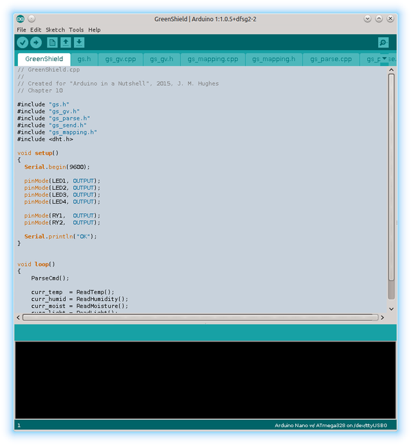
Figure 10-11. The Arduino IDE with the GreenShield files loaded
Table 10-8 lists the files in the GreenShield set. Two files are shared by all the source modules. These are gs.h and gs_gv.h. The global variables defined in gs_gv.cpp that would otherwise be found at the start of a conventional sketch are compiled separately and shared as necessary among the other modules.
| Module | Function |
|---|---|
GreenShield.ino |
Primary module containing |
gs_gv.cpp |
Global variables |
gs_gv.h |
Include file |
gs.h |
Constant definitions ( |
gs_mapping.cpp |
Function mapping |
gs_mapping.h |
Include file |
gs_parse.cpp |
Command parsing |
gs_parse.h |
Include file |
gs_send.cpp |
Data send (to host) functions |
gs_send.h |
Include file |
Organizing a project in this manner makes it easier to deal with just one section at a time without wading through line after line of source code. Once the main section is done, then changes can be made to other modules without interfering with the finished code. This approach also helps in thinking about your software from a modular perspective, and this in turn makes it easier to understand and easier to maintain.
Software description
Figure 10-12 shows the flowchart for the main loop of the software. The
loop() function begins with the “Start” block and it will continue until the
Arduino is powered off. Note that there are three primary functional sections:
command input and response processing, data acquisition, and minimum/maximum
setpoint testing. Also note that the block labeled “Setpoint Test” is one
instance of four blocks, one for each pair of min/max setpoints. In order to
keep the size of the diagram reasonable, only one test section is shown.
The GreenShield.ino source file, shown in Example 10-2, contains the setup()
and loop() functions. The complete GreenShield software can be found on GitHub.
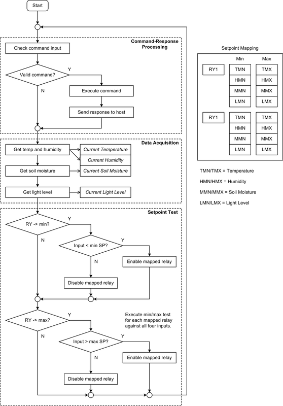
Figure 10-12. GreenShield flowchart
Example 10-2. GreenShield main source file
// GreenShield.ino//// Created for "Arduino: A Technical Reference," 2016, J. M. Hughes// Chapter 10#include "gs.h"#include "gs_gv.h"#include "gs_parse.h"#include "gs_send.h"#include "gs_mapping.h"#include <dht.h>voidsetup(){Serial.begin(9600);pinMode(LED1,OUTPUT);pinMode(LED2,OUTPUT);pinMode(LED3,OUTPUT);pinMode(LED4,OUTPUT);pinMode(RY1,OUTPUT);pinMode(RY2,OUTPUT);Serial.println("OK");}voidloop(){ParseCmd();curr_temp=ReadTemp();curr_humid=ReadHumidity();curr_moist=ReadMoisture();curr_light=ReadLight();ScanMap();}
The Arduino IDE relies on the #include statements to determine which modules
belong in the code set. Even if a source file isn’t directly used by the top-level
module, it must still be included.
The global definitions file gs.h, shown in Example 10-3, defines a set of constants
used by the GreenShield source modules. The #define statements result in a smaller
compiled object, as demonstrated in “Constants”.
Example 10-3. GreenShield global definitions
// gs.h//// Created for "Arduino: A Technical Reference," 2016, J. M. Hughes// Chapter 10#ifndef GSDEFS_H#define GSDEFS_H#define MAXINSZ 12// Input buffer size#define NOERR 0// Error codes#define TIMEOUT 1#define BADCHAR 2#define BADVAL 3#define LED1 2// LED pin definitions#define LED2 3#define LED3 4#define LED4 5#define RY1 6// Relay pin definitions#define RY2 7#define DHT22 8// DHT22 I/O pin#define MPROBE A0// Moisture probe input#define LDRIN A1// LDR input#define MAXRY 2// Maximum num of relays#define MAP_NONE 0// Mapping vectors#define MAP_TEMPMIN 1#define MAP_TEMPMAX 2#define MAP_HUMIDMIN 3#define MAP_HUMIDMAX 4#define MAP_MOISTMIN 5#define MAP_MOISTMAX 6#define MAP_LIGHTMIN 7#define MAP_LIGHTMAX 8#endif
In Example 10-3 the definition of MAXRY is 2. This can be a
larger value if the hardware to support additional relays is present, and
the outputs don’t have to be relays. The include file gs_mapping.h,
shown in Example 10-4, declares the functions for reading the DHT22
and the analog inputs, setting the on/off state of each relay (or all relays),
controlling the status LEDs, and performing a scan through the response
conditions that will control the relays in the function ScanMap().
Example 10-4. GreenShield mapping functions
// gs_mapping.h//// Created for "Arduino: A Technical Reference," 2016, J. M. Hughes// Chapter 10#ifndef GSMAP_H#define GSMAP_HvoidReadDHT22();intReadTemp();intReadHumidity();intReadMoisture();intReadLight();intRyGet(intry);voidRySet(intry,intstate);voidRyAll(intstate);voidLEDControl(intLEDidx);voidScanMap();#endif
The ScanMap() function in gs_mapping.cpp, shown in Example 10-5, is executed
on each cycle of the loop() function in the GreenShield.ino main source file.
It evaluates the analog inputs against a set of configurable limits, and either
enables or disables the relays based on those conditions.
Example 10-5. The GreenShield function map scanner
// NOTE: There are no checks in this code to prevent multiple relays being// mapped to the same operational mode.// Each RY is mapped to one of 8 possible operational modes. Determine the// mapping for a specific relay and see if the enable condition has been// met. This is extensible to any reasonable number of relays.voidScanMap(){for(inti=0;i<MAXRY;i++){if(rymap[i]!=MAP_NONE){switch(rymap[i]){caseMAP_TEMPMIN:if(curr_temp<mintemp){RySet(i,1);}else{RySet(i,0);}break;caseMAP_TEMPMAX:if(curr_temp>maxtemp){RySet(i,1);}else{RySet(i,0);}break;caseMAP_HUMIDMIN:if(curr_humid<minhum){RySet(i,1);}else{RySet(i,0);}break;caseMAP_HUMIDMAX:if(curr_humid>maxhum){RySet(i,1);}else{RySet(i,0);}break;caseMAP_MOISTMIN:if(curr_moist<minmoist){RySet(i,1);}else{RySet(i,0);}break;caseMAP_MOISTMAX:if(curr_moist>maxmoist){RySet(i,1);}else{RySet(i,0);}break;caseMAP_LIGHTMIN:if(curr_light<minlite){RySet(i,1);}else{RySet(i,0);}break;caseMAP_LIGHTMAX:if(curr_light>maxlite){RySet(i,1);}else{RySet(i,0);}break;default:// Do nothingbreak;}}}}
The source module gs_parse.cpp contains one primary function, ParseCmd(),
and a couple of support functions (CntInt() and SendErr()). Example 10-6
shows the contents of gs_parse.h.
Example 10-6. GreenShield parse module include file
// gs_parse.h//// Created for "Arduino: A Technical Reference," 2016, J. M. Hughes// Chapter 10#ifndef GSPARSE_H#define GSPARSE_HvoidParseCmd();intCvtInt(char*strval,intstrt,intstrlen);voidSendErr(interrtype);#endif
The ParseCmd() function is by far one of the largest functions in the GreenShield
code set. If uses a fast descending conditional tree-type parser to determine the
type of an incoming command, and then extract the subfunction code and any parameters.
This function will also execute any immediate commands such as enabling or disabling
relays, returning relay state information, and acquiring and returning analog data
to the control host or a user. Immediate command execution occurs at the endpoints
of the descending tree structure.
Fabrication
It is beyond the scope of this book to provide a step-by-step walk-through for creating schematics and printed circuit boards. This is a high-level description of the steps involved to move from schematic to PCB layout to finished PCB. For the low-level details, I would refer you to the texts listed in Appendix D. A Google search for “CadSoft Eagle” will come back with numerous tutorials. I recommend the tutorials from SparkFun, Adafruit, and, of course, CadSoft.
The Eagle version of the Greenshield schematic is shown in Figure 10-13. Notice the block labeled “ARDUINO_R3_SHIELD.” This is from the SparkFun parts library for Eagle, and it’s intended specifically for creating shields. It is much more convenient than working out the placement of the pin header pads manually later on during the PCB layout phase.
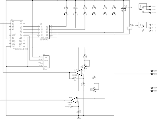
Figure 10-13. GreenShield schematic (Eagle version)
The Eagle schematic editor, like all such tools, takes some time to get used to. It’s not always intuitive or obvious. Normally I use a different tool to create publication-quality line art, including schematics, but to create a PCB it’s useful to have a schematic editor and PCB layout tool that can share data. You can compare Figure 10-13 with Figure 10-9 to see the difference. The Eagle tool, and the Fritzing design tool used in the Switchinator project, can keep schematics and layouts synchronized, whereas a standalone graphics tool for line art and illustrations cannot.
When creating a schematic, make sure you have selected the correct part. For example, the symbol for a resistor is the same no matter if it’s an 0805 SMD (surface-mount) part or a 1/4 watt through-hole component. Sometimes it can be a challenge to find the right part in the schematic editor’s parts library. With Eagle you can use wildcard characters to search the library. When looking for the ULN2003AD part for the GreenShield I entered *2003* and found what I was looking for under the uln-udn category. Sometimes it is necessary to go online and search for a part that someone may have already created. SparkFun, Adafruit, and others have created large libraries of parts that are available to download for free.
Once the schematic is complete the PCB can be generated. Initially the PCB layout is just a jumble of parts and thin connection lines (“air wires,” as they are sometimes called) that form a wiring “rat’s nest.” The rat’s nest shows the point-to-point connections as defined in the netlist (the network list) created from the schematic.
The first step is to move all the parts into the PCB region, and then arrange them. The main objectives when arranging the parts are to locate connectors in the desired locations, group parts by function, and minimize the number of occurrences of crossed rat’s nest lines by rotating parts as necessary. Once this initial step is complete it’s much easier to start creating the traces that will connect the parts.
You can elect to route each trace (or track, as they are sometimes called) by hand, using the rat’s nest wires as a guide, or if you are feeling lucky you can let an autorouter take a shot at it. Eagle does have an autorouter, but I generally don’t use it. Autorouting is typically an iterative process of trying to get a good layout, ripping it up, moving and rotating parts, and then trying it again. After a while it becomes obvious with some designs that it is quicker to just do it manually.
In Eagle, you do not need to manually place a via. (A via transfers a trace from one side of the PCB to the other via a plated-through hole, hence the name.) If you need to transition from the top to the bottom of the PCB (or vice versa), simply change from one side to the other with the layer selection pull-down located at the lefthand side of the trace draw toolbar. Eagle will automatically place a via at that location for you and switch the trace routing to the selected side of the PCB.
The PCB layout is shown in Figure 10-14. The top (component) side is brownish-red, and the bottom (solder) side is blue. If you happen to have the printed version of this book you should see the top side traces as light gray, and the bottom traces as dark gray. The component outlines are in light gray.
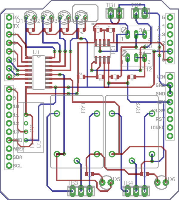
Figure 10-14. GreenShield PCB layout
The files generated by the Eagle CAM (Computer Aided Manufacturing) tool, called “Gerber” files, are used by a PCB fabricator to create the actual PCB. I used the Gerbv tool, part of the gEDA package, to load and view the Gerber files as a last step check. A screenshot of the Gerbv screen is shown in Figure 10-15.
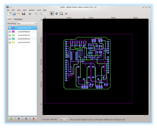
Figure 10-15. Gerbv Gerber file viewer
Note
In order to take advantage of the low-cost service for prototype PCBs, the board outline for the GreenShield was squared to make a rectangle. It might look a little odd, but that won’t affect how it works. You will not see this in the photos, but the layout was originally done using the Arduino shield outline. Converting the corners to right angles took about 5 minutes, and it happened just before the layout was sent off for fabrication. If it really mattered I could have paid a whole lot more money for an edge route and trim operation, or I could have used my own router and done it myself. I opted to just leave it as a rectangle.
It takes about 7 to 10 days to get a finished PCB back. Figure 10-16 shows the bare PCB from the fabricator.
After the parts are soldered onto the PCB it’s always a good idea to spend a few minutes examining both sides for cold solder joints and shorts (called “bridges”) between the pads and traces. I use a standard jeweler’s loupe for this. Figure 10-17 shows what a completely assembled GreenShield looks like.
You might notice that I used stacking headers for the connections to an underlying Arduino or another shield. While it would be awkward to put another shield on the GreenShield (and I would advise against it), I wanted to have some readily accessible test and I/O points.
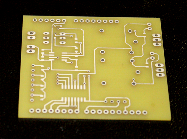
Figure 10-16. Finished bare GreenShield PCB
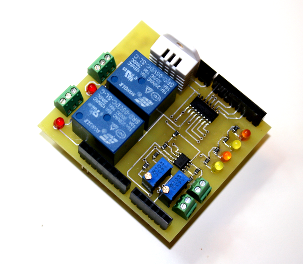
Figure 10-17. Fully populated GreenShield PCB ready to go
Final Acceptance Testing
Surface-mounted parts have their own unique set of potential problems. Before applying power to the GreenShield we should do some quick checks to make sure things are wired correctly and there are no short circuits on the PCB:
- Visual inspection
-
Carefully examine the components on the PCB for solder bridges (solder bridging two pads or between a pad and a trace). Examine the resistors to see if any have an end that may be lifted above the pad and not connected. This can happen when using regular solder and a soldering iron (I used solder paste and a hot air SMD reflow tool). Look at the pads for the ICs (U1 and IC1) to make sure there are no solder bridges between them.
- Component placement
-
There are nine parts that may accidentally be mounted backward. These are the two ICs, the LEDs, and the DHT22 sensor module. The op amp IC may have a dimple or dot to indicate pin 1, but some packages have a beveled edge. In addition to different lead lengths, LEDs will usually have a small flattened area next to the cathode (–) connection.
- Short circuits
-
Using a DMM, preferably with a continuity test function (the beeper mode), check each pair of pins on the LM358 op amp (IC1) for shorts. None of the pins should short to another pin. Now check that the VCC on pin 8 of IC1 is tied to the 5V on the pin header. Also check that pin 4 is tied to one of the ground pins on the pin header.
Repeat this process for the ULN2003A driver (U1). None of the input or output pins should be shorted, pin 8 should be tied to ground, and pin 9 should be connected to the 5V supply.
- Power safety
-
Before connecting the GreenShield to an Arduino board, use a DMM to measure the resistance between the +5V and ground pins on the pin header. You should see a value of no less than about 30K ohms, probably higher. If you get a reading of zero then there is a short somewhere, and it will need to be found and cleared before attempting to power up the GreenShield.
If the GreenShield appears to be acceptable electrically, then we can mount it on an Arduino and apply power. None of the LEDs on the GreenShield should be active initially (unless there is some software already running on the AVR on the Arduino that is controlling the digital I/O pins). Functional testing involves four basic steps:
- Initial functional testing
-
The first part of functional testing is rerunning the same tests as were done with the prototype to test the analog inputs and the DHT22.
Upload the prototype version of the software to the Arduino and open the IDE’s serial monitor window. If everything is working correctly you should see a repeating display with the temperature, humidity, and analog inputs.
- Analog input testing
-
Connect a 470-ohm resistor across the LDR inputs. While observing the continuous output, adjust R12 until the value goes to zero. This demonstrates that this part of the circuit is working correctly. Now repeat this with R8 for the moisture sensor.
- DHT22 testing
-
The output readings from the DHT22 should be what you would expect for the local ambient temperature and humidity. You can use a hot air source (a hair dryer, for instance) to apply warm (not hot!) air to the DHT22 and observe its response.
- Software functional testing
-
Now load the full version of the GreenShield software. You can use the serial monitor window of the Arduino IDE for these tests. This is not an extensive suite of tests, as we’ve already been through some of this earlier with the prototype.
With the full GreenShield software loaded, you should see the word “OK” when it first starts. The GreenShield does not provide a prompt. Enter the command
RY:0:?and the response should beRY:0:0. Now enter the commandRY:0:1. The relay should click and the associated LED should illuminate. Using theRY:0:?command now will returnRY:0:1.We should exercise the rest of the commands as well. We can test the analog limits by shorting or opening the analog inputs. The DHT22 is self-contained, so we don’t need to do a lot with that, but you can set the limits very close and use a hot air source and some steam from a pot of boiling water to verify that the temperature and humidity limits work as expected.
Operation
The GreenShield is physically simple, but it can be functionally complex in terms of how it is integrated into its intended environment. The two main variable inputs, light level and soil moisture, must be calibrated for a specific set of conditions. The range of the light-dependent resistor and the soil moisture probe determine how the midpoints are set using the trimmer potentiometers. Not all LDRs are the same, and there will be a difference between a moisture probe that is just a pair of probes and one with a transistor on it.
There are two basic approaches for adjusting the GreenShield: (1) calibrate the GreenShield for known ranges using references of some sort, or (2) adjust the GreenShield to a specific environment using subjective evaluation (i.e., does the soil feel wet enough?).
The calibrated approach will allow you specify ranges based on hard data, and if you know the ideal soil moisture content for, say, tomatoes, then you can use those values once you have done the calibration and worked out how the ADC readings correspond to moisture content. “Prototype testing” described the basic procedures involved in calibrating the GreenShield for soil moisture and light levels, but you could also use expensive lab equipment as reference sources.
The subjective approach is much easier, and since the primary intent is to avoid killing off your plants it’s probably just as effective after a bit of tweaking. You can adjust the trimmer potentiometers to suit the high and low ends of a subjective evaluation of what is acceptable.
I would suggest some experimentation to see which approach works best for your intended application. I would also suggest taking the time to log data from the GreenShield and build up some profiles that you can study to achieve the best responses for your situation.
Next Steps
The GreenShield is rather minimal, to be sure, but it has a lot of potential. You can use it with a Bluetooth shield or even an Ethernet shield, and remotely monitor the soil conditions of your favorite potted plant, some tomatoes or orchids in a greenhouse, a small outdoor vegetable plot, or a garden in a Mars colony. Connect a standard 24VAC sprinkler system valve to one of the relays and you can automate the watering. You could use the other relay to enable a ventilation fan in a greenhouse to cool it down, or connect it to a heater to keep the interior nice and warm during the winter. And, of course, you could always add another relay or two with an external relay module like those described in Chapter 9.
A microSD shield could also be used if you wanted to strap the GreenShield to a tree in the forest and do some long-term data logging (a solar panel to keep it running would be a good idea, as well). Add a WiFi or GSM shield, and you could scatter GreenShields around a good-sized farm to keep an eye on soil conditions.
Tip
The Greenshield software currently does not save the set-point values if power is lost to the Arduino. One way to get around this is to use the EEPROM in the AVR IC. Refer to Chapter 7 for an overview of the EEPROM library.
Custom Arduino-Compatible Designs
Building an Arduino hardware–compatible PCB is straightforward. In fact, the Arduino folks even provide the schematics and PCB layout files for download. They don’t provide the top or bottom silkscreen masks, however, as these are copyrighted by Arduino.cc and are not covered under an open license. You will need to create your own graphics for the board.
Although much of what you need to build a copy of an Arduino or a shield is readily available, it really isn’t economical to clone an existing Arduino design (either a shield or an MCU board). Unless you own or have access to a PCB production facility and a need for hundreds, or even thousands, of a particular board type, odds are you can find something already fabricated for much less per unit than it would cost you to build it yourself.
The custom approach does make sense if the existing available PCB form factors won’t work for you. Perhaps you want to integrate an Arduino into a larger system, or put an AVR MCU into a uniquely constrained location such as an unmanned aircraft or a robot. If that’s the case, then you might want to consider creating a software-compatible PCB. Your board doesn’t have to look like an Arduino, and there’s no reason it needs to be compatible with existing shields, unless of course you want to use it with a shield from some other source.
As discussed in Chapter 1, a device can be Arduino software compatible without being hardware compatible. All that is needed is a suitable AVR processor, the bootloader firmware, and the Arduino runtime libraries. Even the bootloader firmware is optional. In this section we will design and build an AVR-based DC power controller suitable for use with heavy-duty relays, high-power LEDs, and AC or DC motors.
Programming a Custom Design
If you want to use the Arduino bootloader with a brand-new AVR microcontroller, then you will need to install the bootloader in the chip’s built-in flash memory. Once this is done, you can then treat your custom board like any other Arduino. The tools and procedures involved in uploading executable code to an AVR MCU are covered in “Uploading AVR Executable Code” in Chapter 6. As an alternative to installing the bootloader firmware yourself, many sources sell AVR devices with the Arduino bootloader already installed. Check out Adafruit and SparkFun for ATmega328 ICs with the Arduino bootloader firmware preinstalled. Entering “ATmega328 with Arduino bootloader” into the search box on Amazon.com or eBay returns numerous listings.
Once the bootloader is in place, you can use a USB-to-serial adapter or even a standard serial interface with a suitable RS-232 module like the one shown in Figure 10-26 or a USB-to-serial breakout like the SparkFun device shown in Figure 6-8. For some projects, such as the Switchinator in the next section, the serial interface is not an option for programming the MCU if it is already in use, or if the bootloader is not used. This means you will need to use an ISP (ICSP) programmer such as the Atmel-ICE or the USBtinyISP, both of which are discussed in Chapter 6.
The Switchinator
The device described here, which I am calling the Switchinator (for lack of anything better), is a remote-controlled, 14-channel DC switch with 4 analog input channels. This initial version uses an RS-232 interface and a simple command-response protocol. A possible change for a future version would be the use of an RS-485 interface instead of RS-232.
Definition and Planning
The Switchinator is a standalone PCB that can use a plain ATmega328 or ATmega328p MCU without the Arduino bootloader. It can also use an MCU with the bootloader firmware installed with a serial programmer or a USB-to-serial converter. I have elected to use the Arduino IDE for compiling, and an Adafruit USBtinyISP for the programming. Refer to Chapter 6 for more on programming the MCU.
Core hardware:
-
ATmega328
-
16 MHz crystal clock source
-
ICSP programming interface
-
Integrated 5V DC power supply (9 to 12V DC input)
Inputs and outputs:
-
4 analog inputs
-
14 discrete digital outputs
Control interface:
-
RS-232 host interface
-
Command-response protocol, control host driven
-
Analog readings available on demand
-
Output override by control host
The Switchinator provides 14 discrete digital outputs and 4 analog inputs, and the SPI interface is available through an ICSP pin array. The discrete digital outputs and the analog inputs are terminated at the edge of the PCB using screw terminal blocks. An RS-232 interface is used for communication between the board and a control host computer via the D0 and D1 pins on the MCU.
The PCB is a 100 percent through-hole design. This simplifies the assembly at the expense of a larger PCB and a potentially more challenging PCB layout. The PCB size will not exceed a rectangular size of 100 mm by 140 mm. Mounting holes are located in each corner of the PCB.
The discrete digital outputs of the Switchinator can be used for driving relays, such as the type used on the GreenShield, or controlling up to three unipolar stepper motors using a basic circuit like the one shown in Figure 10-18.
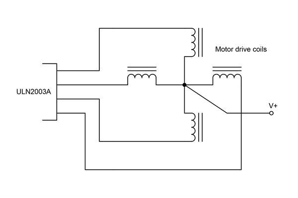
Figure 10-18. ULN2003A connected as stepper driver
The digital outputs of the Switchinator can also drive high-current LEDs, solenoids, or DC motors, as shown in Figure 10-19.
A basic prototype based on a solderless breadboard will be used to develop the initial version of the software. The final version will be completed on the finished hardware.
For the final hardware design I will use Fritzing for schematic capture and PCB layout.
Design
The Switchinator is a single PCB, 124 × 96 mm in size with four corner mounting holes. The final board size is larger than would otherwise be possible with a surface-mount design (it is also larger than the size limits set by the free version of the Eagle tool used for the GreenShield).
There is no enclosure or power supply, which greatly simplifies the design. The Switchinator is entirely self-contained, requiring only an external DC power source for operation.
Functionality
The Switchinator is a digital output device with some analog input capability. Its primary purpose is to switch DC loads, both inductive and noninductive. An ATmega328 AVR MCU is used to decode command inputs and return status data to the control host.
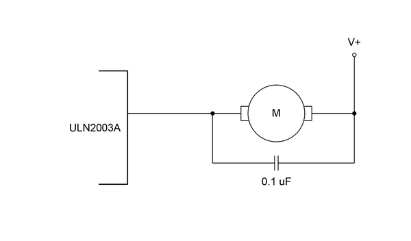
Figure 10-19. ULN2003A DC motor driver
An ATmega328 is used primarily as a command decoder to interface the I/O on the PCB to a host system. Although it has been programmed to act as an I/O device, it could also be programmed to perform autonomous functions based on the analog inputs. By using a linear temperature sensor, such as the LM35, the Switchinator could easily be reprogrammed to serve as a controller for an environmental test chamber or an epoxy curing chamber.
Circuit-wise the Switchinator is comprised of three main sections: MCU, digital I/O, and power supply. Figure 10-20 shows a block diagram of the Switchinator.
The discrete digital outputs are driven by ULN2003A ICs. Four analog inputs are also provided, and the analog reference and AVCC voltages may be supplied either on-board from the internal power supply or externally. Jumpers are used to select the analog voltage sources.
A simple, human-compatible command-response protocol is used to monitor and control the Switchinator.
Hardware
The Switchinator will have 14 digital outputs, each connected to the Darlington outputs of a pair of ULN2003A driver ICs. The ULN2003A drivers have seven channels per IC, and each ULN2003A channel can handle up to 300 mA or more in some cases.
A Microchip MCP23017 I2C digital I/O expander will be used to drive the ULN2003A parts, mainly to avoid using up all of the available digital I/O pins on the AVR MCU. Two of the digital I/O pins on the AVR are used for the serial interface, and two of the analog pins are used for the I2C interface to the MCP23017 IC. The unconnected digital I/O pins are not used, but are available for future expansion.
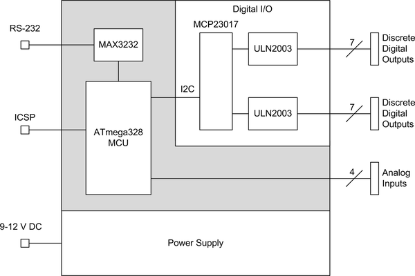
Figure 10-20. Switchinator block diagram
An RS-232 interface is implemented using a MAX232 TTL-to-RS232 transceiver IC. The serial interface will be used to communicate with a host system acting as a master controller. The master controller may be a PC, an Arduino, or some other type of programmable controller with an RS-232 interface. A DB-9 connector is used for the serial interface. This is not a full implementation of RS-232, just the RxD and TxD signals. The Switchinator does not have a USB connector.
The digital outputs and the analog inputs are terminated using 3.5 mm (0.138 inch, 138 mil) pitch screw-type terminal blocks. In addition, two jumpers allow for externally supplied analog V+ and analog reference voltage inputs via a terminal block. A standard PCB-mount DC-barrel type connector is used for DC power. The power input can range from 6 to 12V DC (9V is optimal). A 7805 in a TO-220 package is used for voltage regulation to 5V on the PCB. Figure 10-21 shows the schematic created by Fritzing.
Note
The schematic notation used in Figure 10-21 illustrates what happens when the parts in a tool’s library don’t all follow the same conventions for size and spacing. This is a common issue with open source tools because not every contributed part may have followed the same rules. That doesn’t mean it won’t work; it just looks odd.

Figure 10-21. Switchinator schematic
I used a 16 MHz crystal in the Switchinator for the MCU clock, mainly because I have a bunch of them. For the Switchinator the internal RC oscillator in the AVR would probably do just fine. While the crystal will allow the MCU to run at a specific rate, it also adds some complications with the internal fuse bits the AVR MCU employs for internal configuration. Reading and setting these is discussed in “Setting the AVR MCU Fuse Bits for a 16 MHz Crystal”.
The four analog inputs are brought out to a pair of four-position terminal blocks. The remaining positions are used for V+, ground, and optional analog reference and AVCC inputs. Jumpers JP10 and JP11 are used to select the external voltage sources by removing them from the PCB.
Two of the MCU’s digital pins (D0 and D1) are used for the RS-232 serial interface. Three of the digital pins (D11, D12, and D13) are used for the ICSP programming interface. The remaining digital pins are unassigned. Four of the analog inputs (A0, A1, A2, and A3) are used as general-purpose analog inputs. Pins A4 and A5 are used for the I2C interface between the MCU and the MCP23017 IC. Table 10-10 lists the pin assignments for the Switchinator.
| Pin | Function | Pin | Function | Pin | Function |
|---|---|---|---|---|---|
D0 |
RxD for RS-232 |
D7 |
Not used |
A0 |
General-purpose analog input |
D1 |
TxD for RS-232 |
D8 |
Not used |
A1 |
General-purpose analog input |
D2 |
Not used |
D9 |
Not used |
A2 |
General-purpose analog input |
D3 |
Not used |
D10 |
Not used |
A3 |
General-purpose analog input |
D4 |
Not used |
D11 |
ICSP MOSI |
A4 |
I2C SCL |
D5 |
Not used |
D12 |
ICSP MISO |
A5 |
I2C SDA |
Based on the schematic presented in Figure 10-21 we can generate a detailed parts list as shown in Table 10-11.
| Quantity | Description | Quantity | Description |
|---|---|---|---|
2 |
Capacitor, .1 uF |
4 |
Red LED |
2 |
Capacitor, 10 uf |
1 |
Green LED |
2 |
Capacitor, 27 pF |
5 |
1K ohm resistor, 5%, 1/4 W |
1 |
Capacitor, .001 uF |
1 |
10K ohm resistor, 5%, 1/4 W |
4 |
Capacitor, 1 uF |
1 |
330 ohm resistor, 5%, 1/4 W |
1 |
1N4001 diode |
1 |
Switch, tactile pushbutton |
1 |
MCP23017 I2C I/O expander |
1 |
ATmega328 MCU, 28-pin DIP |
2 |
ULN2003A output driver |
1 |
MAX232 RS232 transceiver, 16-pin DIP |
1 |
Power jack, 5.5 mm barrel |
1 |
7805 voltage regulator, TO-220 |
1 |
AVR ISP connector package, 2 × 3 pins |
1 |
DB9 connector, PCB mount, male |
6 |
Terminal block, 3.5 mm pitch |
1 |
16 MHz crystal |
2 |
2-pin jumper header |
1 |
Software
As with the GreenShield project, the most complex part of the Switchinator is actually the software. Figure 10-23 shows a block diagram of the software.
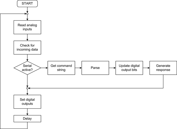
Figure 10-23. Switchinator software block diagram
When the Switchinator is waiting for command input it will send a single “>”
character followed by a space. Responses are preceded with a “<” character and
a space, followed by the response data. The use of the “>” and “<” characters
is mainly for the convenience of software running on a control host system. All
input and output lines are terminated with a newline (
or 0x0A) character.
On every pass through the main loop the analog inputs are read and the values saved. These are returned to the control host when an analog reading is requested, which means they will be updated at the rate of the main loop.
Next, the software checks for incoming serial data. If there is data in the input
buffer the input read function is called to read characters until a newline (a
linefeed character), ASCII value 10 (0x0A or
), is encountered. The parser
then extracts the command from the string, parses out the parameters, and executes
the commanded operation.
Control of the Switchinator is done using a simple command-response protocol. For every command or query sent by the control host the Switchinator will respond with a single response. The Switchinator will never initiate a communications transaction with the control host. The complete command-response protocol is shown in Table 10-12.
| Command | Response | Description | In/out format |
|---|---|---|---|
|
|
Get analog input |
Hex |
|
|
Read status of output |
Hex (0 or 1) |
|
OK |
Write 0 or 1 to output |
Hex |
|
OK |
Set all outputs to hex value |
4-digit hex |
G:? |
|
Get hex value for all outputs |
4-digit hex |
The command set is simple, and only the W (write) command uses two
parameters instead of just one. All parameter and response values are in
hexadecimal notation. This allows digital port numbers to be single hex
digits, while the analog input values (the A command) and the mass set
and retrieve commands (S, or set all ports, and G, get all ports,
respectively) use four-digit hex values. The digits 0 and 1 are nominally
in hex, but they are the same in decimal notation.
Error detection is handled by examining the string returned from the
Switchinator. If the A, R, or G commands return the string sent, then
an error occurred. If the S or W commands encounter an error they will
return the original string; if they succeed, then the string “OK” will
be returned.
The A command accepts a single digit from 0 to 3, and the analog data is
the actual value returned by the ADC in the AVR MCU. It is returned as a
hexadecimal value of 1 to 3 digits, with 0x3FF as the maximum possible
value.
The R and W commands have the specific digital output port number
in the form of a single hex digit, ranging from 0 to 0xF (15). Output
channels 7 and 0xF are used for on-board LEDs; they are not brought out
through the ULN2003A drivers.
Notice in Table 10-12 that to control or get the status of more
than one output the S and G commands are used with a hexadecimal value. With
this scheme we can enable (set to an on state) noncontiguous outputs, or
read back the state of all the outputs.
If, for example, we wanted to set outputs 5, 6, 12, and 13 to an on state,
then we would send the value 3060h, which translates to binary as follows:
Bit   | 15   11    7    3  0
---------+----+----+----+---
Binary|  0011 0000 0110 0000
Hex   |     3    0    6    0
Remember that the channel numbering is zero-based.
Tip
Sending a hexadecimal value will cause outputs to change state to match the command value. That means that if an output is on, and the command value has a zero in that position, it will be set to off.
Use a read-modify-write operation (get bits, change data, set bits) to set or
clear a specific output bit without disturbing other bits. This is how the W
command works.
The last step in the loop transfers the digital output state bits to the hardware. If no changes have been made since the last update the outputs will not do anything; otherwise, bits that have been changed will appear as changes in the on or off state of the ULN2003A outputs.
Prototype
The prototype mainly focuses on the RS-232 interface and the command-response control protocol, so the prototype hardware consists mainly of an ATmega328 mounted on a solderless breadboard. An RS-232 adapter module is used as a stand-in for the MAX232 in the final board. Figure 10-25 shows the prototype fixture.
The RS-232 module is a self-contained unit with a MAX3232 IC. This part is functionally equivalent to the MAX232 used in the Switchinator. The MAX3232 is nominally a 3.3V part, although it is 5V tolerant. It is also slightly more expensive than the MAX232. Figure 10-26 shows a close-up of the RS-232 interface module.
These modules are available from multiple vendors for between $3 and $6. A Google search for “arduino rs232 module” or “arduino rs232 converter” will turn up numerous results.
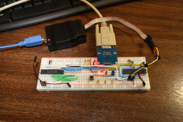
Figure 10-25. Switchinator prototype fixture
Figure 10-26. RS-232 interface module
Most desktop PCs still have a single RS-232 port and a DB-9 connector on the rear panel, but if you have a late-model notebook PC you may not have a serial port available. To get around this, you can use a USB-to-RS232 adapter. These range in price from around $4 to over $30, with some specialty types costing even more. For more details about RS-232 and the connectors used with it, I would recommend my books Real World Instrumentation with Python and Practical Electronics: Components and Techniques (see Appendix D). Both contain sections dealing specifically with RS-232, DB-9 connectors, gender changers, and how to wire a DB-9 to allow RxD/TxD communications without the handshaking signals.
Prototype software
The prototype software is essentially the same as the final version, only without the code to set the digital outputs via the MCP23017. The main focus with the prototype is the implementation of the command-response protocol. The states of the outputs are represented as bits in a 16-bit word in the software.
“Software” contains a detailed discussion of the software, so rather than put it here and possibly repeat parts of it later, I would recommend that you look there for the details. The software is compiled using the Arduino IDE and then uploaded to the AVR MCU using an Adafruit USBtinyISP ICSP interface device.
I used the Arduino IDE to handle compiling chores, but I disabled its internal editor in the Preferences dialog. This allowed me to use a different editor (I write commercial and scientific software for living, so I have some definite preferences when it comes to text editors—I’m not a big fan of the editor in the Arduino IDE). The board was set to “Duemilanove with ATmega328” and the programmer to “USBtinyISP.”
On a Linux system the USBtinyISP doesn’t use a pseudo-serial port, but instead
communicates directly with the underlying USB I/O subsystem. Attempting to run
the Arduino IDE with the programmer will initially result in a permissions error.
You can run the Arduino IDE using sudo, but this is not a convenient way to
transfer your code. To get around this you need to add an access rule for the
udev handler.
Create a file in /etc/udev/rules.d called tinyusb.rules, and add the following string to it:
SUBSYSTEM=="usb", ATTR{product}=="USBtiny", ATTR{idProduct}=="0c9f",
ATTRS{idVendor}=="1781", MODE="0660", GROUP="dialout"
I used vi and sudo to accomplish this:
sudo vi tinyusb.rules
Then restart the udev subsystem to make the new rule take effect:
sudo restart udev
You could also use some other type of programming device (even another Arduino, as described in Chapter 6). I have an Atmel-ICE, but ended up not using it under Linux because I don’t have the latest version of AVRDUDE and I was too lazy to build it and fiddle with the configuration files. It works with Atmel’s AVR Studio software, so if you’re using Windows you might want to take that route. On my Linux system the little gadget from Adafruit works just fine.
Using the upload icon in my version of the IDE causes it to try to start a transfer using the USB-to-serial method built into Arduino boards (and supported by a USB-to-serial converter like the one mentioned earlier). This won’t work with the USBtinyISP, so instead I use the File→Upload Using Programmer option.
One thing I noticed is that the AVRDUDE transfer software is slow getting started, but runs quickly once it has established a solid communications link with the AVR MCU. You can see this both in the Arduino IDE and by running AVRDUDE from the command line. Don’t panic if it looks like things are hung; they aren’t. If there is a problem AVRDUDE will eventually time out and tell you what went wrong.
Prototype testing
Testing the prototype is straightforward, and this section describes tests to specifically exercise the command parser. The ability to successfully interact with the software will demonstrate that the RS-232 interface portion of the code is working correctly. It is assumed that the external RS-232 transceiver works as intended.
First, the output (OUT), status (ST), and input (AN) commands are tested. The
OUT:A:1 and OUT:A:0 commands are used to set the outputs either all on or
all off. The state of each output is held in memory so there is no need for
output hardware at this point.
With the ST:n:? command the n parameter is a single digit from 0 to 13 (D in hex).
Note that the OUT:n:0 and OUT:n:1 command forms also use a single digit.
If the software is working correctly it should be possible to set all outputs
to off (0), and then selectively enable and disable any of the outputs from
0 to 13 without altering any of the other outputs.
The analog input (AN) command is tested by applying a variable voltage source (0 to
5V only) to A0 through A3 and requesting the value. As the input voltage is changed
the returned data should change as well. The input value is returned as a three-digit
hexadecimal value. The two most significant bits are always 0 (the AVR MCU only
has a 10-bit ADC).
The SP:val and GP:? commands use a four-digit hexadecimal value, as described
earlier. Testing will involve setting all odd outputs on and all even-numbered
outputs off, then checking the states of each using the ST command. Then the odd-numbered outputs will be set to off and the even outputs set to on, and the states of
the output bits will again be checked using the ST command.
Software
Although it is possible, and often advisable, to create a simplified version of the software for use with the prototype, in the case of the Switchinator it begins life as a multifile code set. The main file is, of course, Switchinator.ino. The other files in the set contain the global definitions, the global variables, the command parser, the response generator, and the I/O control code. The I/O module, sw_io.cpp, is not necessary in the prototype version of the software.
Source code organization
The Switchinator source code is comprised of eight files, or modules, described in Table 10-15. The primary module, Switchinator.ino, contains the setup() and loop() functions. It also references
the other modules using #include statements.
| Module | Function |
|---|---|
Switchinator.ino |
Primary module containing |
sw_defs.h |
Constant definitions ( |
sw_gv.cpp |
Global variables |
sw_gv.h |
Include file |
sw_io.cpp |
Hardware I/O functions |
sw_io.h |
Include file |
sw_parse.cpp |
Command parsing |
sw_parse.h |
Include file |
Full listings of all the Switchinator source files are available on GitHub.
Software description
As with any Arduino program, the action begins in the main sketch file. The contents of the Switchinator.ino main file are listed in Example 10-9.
Example 10-9. Switchinator.ino
//-------------------------------------------------------------------// Switchinator.ino//// Created for "Arduino: A Technical Reference," 2016, J. M. Hughes// Chapter 10//-------------------------------------------------------------------#include <stdint.h>#include <Wire.h>// the MCP23017 library#include <IOexp.h>// Include all source modules#include "sw_parse.h"#include "sw_gv.h"#include "sw_defs.h"#include "sw_io.h"// define the clock rate#define F_CPU 16000000ULboolwaitinput=false;boolusedelay=false;voidsetup(){Serial.begin(9600);// Startup banner and start flag stringSerial.println();Serial.println("SWITCHINATOR V1.0");Serial.println("READY");Serial.println("####");// Start flag}voidloop(){// Read analog inputs and update GV arrayScanAnalog();// Emit only one input promptif(!waitinput){waitinput=true;Serial.(INPPCH);}// Check for incoming commandif(GetCommand()){waitinput=false;// Reset input prompt output flag}else{ClearBuff(0);ResetBuffLen();// if no input then enable loop delayusedelay=true;}// Parse command (if received)if(DecodeCommand()){// Return response to control host (or user)Serial.println();Serial.(OUTPCH);Serial.println(gv_cmdinstr);}// Update the digital outputs using state bitsSetDigBits();// delay briefly if no input detectedif(usedelay){usedelay=false;delay(50);}}
The setup() function contains the usual initialization statements along with
the initial startup message. The loop() function continuously updates the
output bits and checks for incoming commands from a control host system via
the GetCommand() function in the SW_parse.cpp module.
Referring back to Figure 10-23 the block “Get command string” refers
to the GetCommand() function in the sw_parse.cpp module, the “Parse” and
“Generate response” function blocks are contained in the DecodeCommand()
function, and “Update digital output bits” is the SetDigBits() function in
the sw_io.cpp module. Figure 10-27 shows how the output bit state buffer,
gv_statebits, is used to hold an internal representation of the output bits. All
bit modification functions operate on gv_statebits, not on the actual digital
outputs.
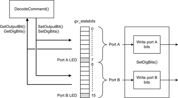
Figure 10-27. Switchinator’s virtual bit buffer in operation
Note that writing 0x00 to either port A or port B will also enable the associated port LED. Writing an 0xFF to either port will disable the LED. The output bits are updated about once every 50 ms if no serial input is present to be parsed and decoded.
Fabrication
For the hardware design I used the Fritzing design tool. This is an integrated virtual breadboard, schematic capture, and PCB layout tool that is easy to install and relatively easy to use. Fritzing has a large and vibrant user base and lots of preloaded parts in its library, and best of all, it’s free. Some Linux distributions may have an older version of Fritzing in their repository, but you can download the latest version from http://fritzing.org/home. I used version 0.8.5 running on a Kubuntu 14.04 LTS Linux system. There are also versions of Fritzing available for Windows and Mac OS X.
Compared to other tools I’ve worked with over the years, I was pleasantly surprised at how easy Fritzing’s user interface was to use. To be honest, I wasn’t all that impressed by the autorouter, but then I’ve seen high-end autorouters struggle with things I thought would be easy. And autorouting software is very challenging to program, so I wasn’t expecting a miracle. I ended up doing the layout manually (and it shows, I’m sure). The DRC (design rules check) worked well, and while the schematic editor had some unique quirks, it too was completely usable. My main complaint with Fritzing is the parts library. It seems that not everyone is on the same page when it comes to dimensions for schematic symbols, so parts from one contributed library might be really small, while the stock parts supplied with Fritzing are actually nice, large symbols. You will see this when you look at the schematic in Figure 10-21. The upshot is that unless all the parts in a tool’s library—both the symbols and the layout footprints—adhere to the same dimensioning constraints, it is difficult to get perfectly orthogonal lines or traces without doing some serious fiddling with the grid sizing and snap functions.
Once the schematic (shown in Figure 10-21) is complete, the PCB layout work can begin. The first time the PCB layout appears it will have no traces, just the rat’s nest lines to indicate which pins are connected on the parts. In Figure 10-28 I’ve already placed the components where I think they should go, and Fritzing is showing some of the rat’s nest lines. Clicking and holding on a pin on any part will highlight all the other places it should be connected in bright yellow.
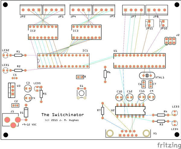
Figure 10-28. PCB after parts placement, but before routing
The components are grouped by function: the power supply is in the lower-left part of the PCB; the MCP23017 and the two ULN2003A parts are in the upper-left region; the MCU, crystal, ICSP connector, and analog inputs are located at the upper right; and the serial interface is located at the bottom right of the layout.
You might notice that I reversed the analog input terminal block symbols to simplify the wiring. They will still be mounted correctly, and since a prototype PCB like this doesn’t have a top layer silkscreen it won’t make any difference.
Some of the trace routing is rather tortuous, due mainly to the use of through-hole parts. Vias are used to shift the traces between the top and bottom sides of the PCB in order to route without collisions. Figure 10-29 shows the final version of the PCB that went out for fabrication.
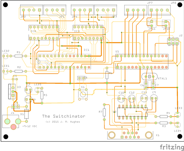
Figure 10-29. Final version of the Switchinator PCB layout
Before sending out the Gerber files, I checked the design with the Gerbv tool (which was introduced earlier with the GreenShield). A screenshot is shown in Figure 10-30.
Fortunately, the fabrication house (Advanced Circuits) discovered two pads that were almost, but not quite, connected. It would have been easy to fix on the workbench, but it would have been a challenge to find the problems. Good thing someone was paying attention and checked the layouts.
The Switchinator is a through-hole PCB, so assembly is straightforward. Figure 10-31 shows the bare PCB before any parts are installed.
The first parts to solder into place are the DC jack and the 7805 regulator, along with the associated power supply components, consisting of D1, C2, C3, C4, and C5. Note that there is no C1 (it vanished in an earlier revision). To test the power supply we also need to install R5 and LED5. Once these parts are installed we can connect a 9 to 12V DC wall supply via the DC power jack and verify that the regulator is producing 5 volts DC at the anode of LED5 (which should be glowing).
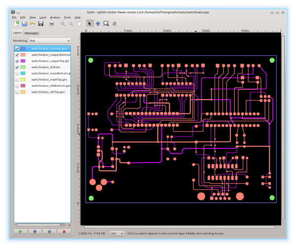
Figure 10-30. Gerbv PCB layout display
Next we will install the RS-232 connector, labeled X1 in the schematic; U2 (the MAX232 IC); and C9, C10, C11, and C12. Using the prototype breadboard we can attach the Rx and Tx signals from pins 2 and 3 of the MCU to the U1 pins 2 and 3 on the PCB. Then we run the software already on the AVR MCU and verify that our integrated RS-232 is working correctly. Remember to tie the ground and 5V DC power from the PCB to the breadboard (and disconnect the breadboard’s power supply, of course).
With the power supply and the RS-232 interface installed and running, we can now install U1 (the MCU), IC1, IC2, and IC3. LED1, LED2, R1, and R2 can also be soldered in place, along with the six terminal blocks. Next, the crystal, C6, C7, C8, R3, R4, R6, LED3, and LED4 are installed. The reset switch, S1, and the ICSP connector are the last things to mount on the PCB.
Figure 10-31. The bare Switchinator PCB
Figure 10-32 shows the finished PCB with everything installed and ready to go. The maximum current that the ULN2003A drivers can supply is determined by the power supply and by the ratings for the ICs themselves. The datasheet states that the ULN2003A is capable of supplying around 300 mA per channel, or about 2.1A per IC. By comparison, the ATmega328 and the MCP23017 draw very little current, so the major concern will always be the ULN2003A devices. A power source capable of supplying at least 5A should be more than sufficient if you want to use the Switchinator for something like a small CNC tool or an LED display controller.
Acceptance Testing
Final testing of the finished Switchinator is largely a repeat of the testing done with the prototype. The big difference now is that there are two ULN2003A drivers and an integrated RS-232 interface based on a MAX232 IC. The power supply also needs to be tested, as well as the analog inputs.
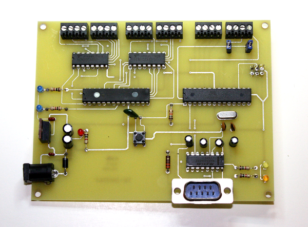
Figure 10-32. The finished Switchinator
Next Steps
Not all of the discrete digital I/O pins on the MCU have been used; 10 pins (including 6 capable of PWM output) are available. I didn’t bring these out due to space constraints on the PCB, but it should be possible to modify the PCB for a couple of six-position pin socket headers. It will, however, require some clever use of vias to get the traces routed through the resulting traffic jam around the MCU.
The SPI interface is available on pins D11, D12, and D13, and these are wired to the ICSP connector. If you select an unused pin for the SS line you can connect an SPI module to the Switchinator. The analog pins can be used as digital I/O pins by referencing them as pins D14 through D19.
You may have also noticed that there is no fuse, and no input protection for the analog inputs. For an example of analog input protection, see Chapter 11 and the input circuit used for the signal generator.
Resources
This chapter has covered a lot of ground, and taken a few leaps of faith. Here are some resources that will help shed more light on the topics only touched on briefly in the text:
- Reference texts
-
There are numerous texts available that cover all aspects of electronics. These are some that I am particularly fond of that relate directly to material covered in this chapter (refer to Appendix D for ISBN numbers and even more recommended texts):
-
Jan Axelson, Making Printed Circuit Boards
-
Paul Horowitz and Winfield Hill, The Art of Electronics, 2nd Edition
-
J. M. Hughes, Practical Electronics: Components and Techniques
-
J. M. Hughes, Real World Instrumentation with Python
-
Simon Monk, Fritzing for Inventors
-
Matthew Scarpino, Designing Circuit Boards with EAGLE
-
- Schematic capture and PCB layout
-
Fritzing and Eagle aren’t the only electronics CAD tools available, but they are commonly encountered when downloading schematics or board layouts created and posted online by others. Fritzing is free and open source, and there are many sources for parts definitions beyond those that are supplied with it. It is easy to learn and easy to use, and for Arduino projects it is a good choice.
The free version of Eagle has the features found in the commercial versions of the tool, so it presents a clear upgrade path when you want to explore the world of professional CAD/CAM tools for electronics. Just remember that the free Eagle has some limitations, and it’s not intended to be used in any situation where you plan to make money from your work. For that you will need to purchase a commercial license.
Some other CAD tool options are the open source Linux tools like the gEDA suite and KiCad, both of which have features comparable with commercial products. For more information on the tools mentioned here, see their websites:
- PCB fabricators
-
There are many PCB fabrication firms that offer low prices and quick turn-around times. Check around on the Web, and if you happen to live in a large metropolitan area, also be sure to take a look at what services are available locally. I’ve listed Advanced Circuits mainly because I am most familiar with them, and I’ve never had a problem with their work. The folks at Fritzing.org offer a PCB fabrication service, too (you can access it from within the Fritzing tool):
- Component sources
-
Throughout this book I’ve referred to many different sources for everything from single components to modules and complete Arduino boards. The following companies are some starting points to consider (for more pointers, see Appendix C):