
Detailed Models
This appendix contains further models and information that can be useful for some readers of this book. For example, the protocols section may be useful for hardware designers who wish to work in networking but need a quick self-contained overview of protocols such as TCP and IP to orient themselves. On the other hand, the hardware section provides insights that may be useful for software designers without requiring a great deal of reading. The switch section provides some more details about switching theory.
A.1 TCP AND IP
To be self-contained, Section A.1.1 provides a very brief sketch of how TCP operates, and Section A.1.2 briefly describes how IP routing operates.
A.1.1 Transport Protocols
When you point your Web browser to www.cs.ucsd.edu, your browser first converts the destination host name (i.e., cs.ucsd.edu) into a 32-bit Internet address, such as 132.239.51.18, by making a request to a local DNS name server [Per92]; this is akin to dialing directory assistance to find a telephone number. A 32-bit IP address is written in dotted decimal form for convenience; each of the four numbers between dots (e.g., 132) represents the decimal value of a byte. Domain names such as cs.ucsd.edu appear only in user interfaces; the Internet transport and routing protocols deal only with 32-bit Internet addresses.
Networks lose and reorder messages. If a network application cares that all its messages are received in sequence, the application can subcontract the job of reliable delivery to a transport protocol such as transmission control protocol (TCP). It is the job of TCP to provide the sending and receiving applications with the illusion of two shared data queues in each direction — despite the fact that the sender and receiver machines are separated by a lossy network. Thus whatever the sender application writes to its local TCP send queue should magically appear in the same order at the local TCP receive queue at the receiver, and vice versa.
Since Web browsers care about reliability, the Web browser at sender S (Figure A.1) first contacts its local TCP with a request to set up a connection to the destination application. The destination application is identified by a well-known port number (such as 80 for Web traffic) at the destination IP address. If IP addresses are thought of as telephone numbers, port numbers can be thought of as extension numbers. A connection is the shared state information — such as sequence numbers and timers — at the sender and receiver TCP programs that facilitate reliable delivery.
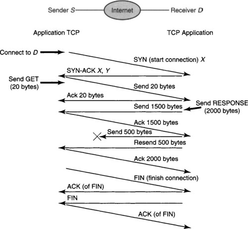
Figure A.1 is an example of a time–space figure, with time flowing downward and space represented horizontally. A line from S to D that slopes downward represents the sending of a message from S to D, which arrives at a later time.
To set up a connection, the sending TCP (Figure A.1) sends out a request to start the connection, called a SYN message, with a number X the sender has not used recently. If all goes well, the destination will send back a SYN-ACK to signify acceptance, along with a number Y that the destination has not used before. Only after the SYN-ACK is the first data message sent.
The messages sent between TCPs are called TCP segments. Thus to be precise, the following models will refer to TCP segments and to IP packets (often called datagrams in IP terminology).
In Figure A.1, the sender is a Web client, whose first message is a small (say) 20-byte HTTP GET message for the Web page (e.g., index.html) at the destination. To ensure message delivery, TCP will retransmit all segments until it gets an acknowledgment. To ensure that data is delivered in order and to correlate acks with data, each byte of data in a segment carries a sequence number. In TCP only the sequence number of the first byte in a segment is carried explicitly; the sequence numbers of the other bytes are implicit, based on their offset.
When the 20-byte GET message arrives at the receiver, the receiving TCP delivers it to the receiving Web application. The Web server at D may respond with a Web page of (say) 1900 bytes that it writes to the receiver TCP input queue along with an HTTP header of 100 bytes, making a total of 2000 bytes. TCP can choose to break up the 2000-byte data arbitrarily into segments; the example of Figure A.1 uses two segments of 1500 and 500 bytes.
Assume for variety that the second segment of 500 bytes is lost in the network; this is shown in a time–space picture by a message arrow that does not reach the other end. Since the receiver does not receive an ACK, the receiver retransmits the second segment after a timer expires. Note that ACKs are cumulative: A single ACK acknowledges the byte specified and all previous bytes. Finally, if the sender is done, the sender begins closing the connection with a FIN message that is also acked (if all goes well), and the receiver does the same.
Once the connection is closed with FIN messages, the receiver TCP keeps no sequence number information about the sender application that terminated. But networks can also cause duplicates (because of retransmissions, say) of SYN and DATA segments that appear later and confuse the receiver. This is why the receiver in Figure A.1 does not believe any data that is in a SYN message until it is validated by receiving a third message containing the unused number Y the receiver picked. If Y is echoed back in a third message, then the initial message is not a delayed duplicate, since Y was not used recently. Note that if the SYN is a retransmission of a previously closed connection, the sender will not echo back Y, because the connection is closed.
This preliminary dance featuring a SYN and a SYN-ACK is called TCP’s three-way handshake. It allows TCP to forget about past communication, at the cost of increased latency to send new data. In practice, the validation numbers X and Y do double duty as the initial sequence numbers of the data segments in each direction. This works because sequence numbers need not start at 0 or 1 as long as both sender and receiver use the same initial value.
The TCP sequence numbers are carried in a TCP header contained in each segment. The TCP header contains 16 bits for the destination port (recall that a port is like a telephone extension that helps identify the receiving application), 16 bits for the sending port (analogous to a sending application extension), a 32-bit sequence number for any data contained in the segment, and a 32-bit number acknowledging any data that arrived in the reverse direction. There are also flags that identify segments as being SYN, FIN, etc. A segment also carries a routing header1 and a link header that changes on every link in the path.
If the application is (say) a videoconferencing application that does not want reliability guarantees, it can choose to use a protocol called UDP (user datagram protocol) instead of TCP. Unlike TCP, UDP does not need acks or retransmissions, because it does not guarantee reliability. Thus the only sensible fields in the UDP header corresponding to the TCP header are the destination and source port numbers. Like ordinary mail versus certified mail, UDP is cheaper in bandwidth and processing but offers no reliability guarantees. For more information about TCP and UDP, Stevens [Ste94] is highly recommended.
A.1.2 Routing Protocols
Figure A.2 shows a more detailed view of a plausible network topology between Web client S and Web server D of Figure A.1. The source is attached to a local area network such as an Ethernet, to which is also connected a router, R1. Routers are the automated post offices of the Internet, which consult the destination address in an Internet message (often called a packet) to decide on which output link to forward the message.

In the figure, the source S belongs to an administrative unit (say, a small company) called a domain. In this simple example, the domain of S consists only of an Ethernet and a router, R1, that connects to an Internet service provider (ISP) through router R2. Our Internet service provider is also a small outfit, and it consists only of three routers, R2, R3, and R4, connected by fiber-optic communication links. Finally, R4 is connected to router R5 in D’s domain, which leads to the destination, D.
Internet routing is broken into two conceptual parts, called forwarding and routing. First consider forwarding, which explains how packets move from S to D through intermediate routers.
When S sends a TCP packet to D, it first places the IP address of D in the routing header of the packet and sends it to neighboring router, R1. Forwarding at endnodes such as S and D is kept simple and consists of sending the packet to an adjoining router. Rl realizes it has no information about D and so passes it to ISP router R2. When it gets to R2, R2 must choose to send the packet to either R3 or R4. R2 makes its choice based on a forwarding table at R2 that specifies (say) that packets to D should be sent to R4. Similarly, R4 will have a forwarding entry for traffic to D that points to R5. A description of how forwarding entries are compressed using prefixes can be found in Section 2.3.2. In summary, an Internet packet is forwarded to a destination by following forwarding information about the destination at each router. Each router need not know the complete path to D, but only the next hop to get to D.
While forwarding must be done at extremely high speeds, the forwarding tables at each router must be built by a routing protocol. For example, if the link from R2 to R4 fails, the routing protocol within the ISP domain should change the forwarding table at R2 to forward packets to D to R3. Typically, each domain uses its own routing protocol to calculate shortestpath routes within the domain. Two main approaches to routing within a domain are distance vector and link state.
In the distance vector approach, exemplified by the protocol RIP [Per92], the neighbors of each router periodically exchange distance estimates for each destination network. Thus in Figure A.2, R2 may get a distance estimate of 2 to D’s network from R3 and a distance estimate of 1 from R4. Thus R2 picks the shorter-distance neighbor, R4, to reach D. If the link from R2 to R4 fails, R2 will time-out this link, set its estimate of distance to D through R4 to infinity, and then choose the route through R3. Unfortunately, distance vector takes a long time to converge when destinations become unreachable [Per92],
Link state routing [Per92] avoids the convergence problems of distance vector by having each router construct a link state packet listing its neighbors. In Figure A.2, for instance, R3’s link state packet (LSP) will list its links to R2 and R4. Each router then broadcasts its LSP to all other routers in the domain using a primitive flooding mechanism; LSP sequence numbers are used to prevent LSPs from circulating forever. When all routers have each other’s LSP, every router has a map of the network and can use Dijkstra’s algorithm [Per92] to calculate shortest-path routes to all destinations. The most common routing protocol used within ISP domains is a link state routing protocol called open shortest path first (OSPF) [Per92].
While shortest-path routing works well within domains, the situation is more complex for routing between domains. Imagine that Figure A.2 is modified so that the ISP in the middle, say, ISP A, does not have a direct route to D’s domain but instead is connected to ISPs C and E, each of which has a path to D’s domain. Should ISP A send a packet addressed to D to ISP C or E? Shortest-path routing no longer makes sense because ISPs want to route based on other metrics (e.g., dollar cost) or on policy (e.g., always send data through a major competitor, as in so-called “hot potato” routing).
Thus interdomain routing is a more messy kettle of fish than routing within a domain. The most commonly used interdomain protocol today is called the border gateway protocol (BGP) [Ste99], which uses a gossip mechanism akin to distance vector, except that each route is augmented with the path of domains instead of just the distance. The path ostensibly makes convergence faster than distance vector and provides information for policy decisions.
To go beyond this brief sketch of routing protocols, the reader is directed to Interconnections by Radia Perlman [Per92] for insight into routing in general and to BGP-4 by John Stewart [Ste99] as the best published textbook on the arcana of BGP.
A.2 HARDWARE MODELS
For completeness, this section contains some details of hardware models that were skipped in Chapter 2 for the sake of brevity. These detailed models are included in this section to provide somewhat deeper understanding for software designers.
A.2.1 From Transistors to Logic Gates
The fundamental building block of the most complex network processor is a transistor (Figure A.3). A transistor is a voltage-controlled switch. More precisely, a transistor is a device with three external attachments (Figure A.3): a gate, a source, and a drain. When an input voltage I is applied to the gate, the source–drain path conducts electricity; when the input voltage is turned off, the source–drain path does not conduct. The output O voltage occurs at the drain. Transistors are physically synthesized on a chip by having a polysilicon path (gate) cross a diffusion path (source–drain) at points governed by a mask.
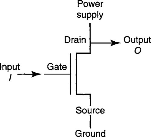
The simplest logic gate is an inverter (also known as a NOT gate). This gate is formed (Figure A.3) by connecting the drain to a power supply and the source to ground (0 volts). The circuit functions as an inverter because when I is a high voltage (i.e., I = 1), the transistor turns on, “pulling down” the output to ground (i.e., O = 0). On the other hand, when I = 0, the transistor turns off, “pulling up” the output to the power supply (i.e., O = 1). Thus an inverter output flips the input bit, implementing the NOT operation. Although omitted in our pictures, real gates also add a resistance in the path to avoid “shorting” the power supply when I = 1, by connecting it directly to ground.
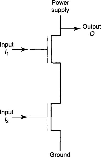
The inverter generalizes to a NAND gate (Figure A.4) of two inputs I1 and I2 using two transistors whose source–drain paths are connected in series. The output O is pulled down to ground if and only if both transistors are on, which happens if and only if both I1 and I2 are 1. Similarly, a NOR gate is formed by placing two transistors in parallel.
A.2.2 Timing Delays
Figure A.3 assumes that the output changed instantaneously when the input changed. In practice, when I is turned from 0 to 1, it takes time for the gate to accumulate enough charge to allow the source–drain path to conduct. This is modeled by thinking of the gate input as charging a gate capacitor (C) in series with a resistor (R). If you don’t remember what capacitance and resistance are, think of charge as water, voltage as water pressure, capacitance as the size of a container that must be filled with water, and resistance as a form of friction impeding water flow. The larger the container capacity and the larger the friction, the longer the time to fill the container. Formally, the voltage at time t after the input I is set to V is V(1 – e−t/RC). The product RC is the charging time constant; within one time constant the output reaches 1 – 1/e = 66% of its final value.
In Figure A.3, notice also that if I is turned off, output O pulls up to the power supply voltage. But to do so the output must charge one or more gates to which it is connected, each of which is a resistance and a capacitance (the sum of which is called the output load). For instance, in a typical 0.18-micron process,2 the delay through a single inverter driving an output load of four identical inverters is 60 picoseconds.
Charging one input can cause further outputs to charge further inputs, and so on. Thus for a combinatorial function, the delay is the sum of the charging and discharging delays over the worst-case path of transistors. Such path delays must fit within a minimum packet arrival time. Logic designs are simulated to see if they meet timing using approximate analysis as well as accurate circuit models, such as Spice. Good designers have intuition that allows them to create designs that meet timing. A formalization of such intuition is the method of logical effort [SSH99], which allows a designer to make quick timing estimates. Besides the time to charge capacitors, another source of delay is wire delay.
A.2.3 Hardware Design Building Blocks
This section describes some standard terminology for higher-level building blocks used by hardware designers that can be useful to know.
PROGRAMMABLE LOGIC ARRAYS AND PROGRAMMABLE ARRAY LOGICS
A programmable logic array (PLA) has the generality of a software lookup table but is more compact. Any binary function can be written as the OR of a set of product terms, each of which is the AND of a subset of (possibly complemented) inputs. The PLA thus has all the inputs pass through an AND plane, where the desired product terms are produced by making the appropriate connections. The products are then routed to an OR plane. A designer produces specific functions by making connections within the PLA. A more restrictive but simpler form of PLA is a PAL (programmable array logic).
STANDARD CELLS
Just as software designers reuse code, so also do hardware designers reuse a repertoire of commonly occurring functions, such as multiplexors and adders.
The functional approach to design is generally embodied in standard cell libraries and gate array technologies, in which a designer must map his or her specific problem to a set of building blocks offered by the technology. At even higher abstraction levels, designers use synthesis tools to write higher-level language code in Verilog or VHDL for the function they wish to implement. The VHDL code is then synthesized into hardware by commercial tools. The trade-off is reduced design time, at some cost in performance. Since a large fraction of the design is not on the critical path, synthesis can greatly reduce time to market. This section ends with a networking example of the use of reduction for a critical path function.
A.2.4 Memories: The Inside Scoop
This section briefly describes implementation models for registers, SRAMs, and DRAMs.
REGISTERS
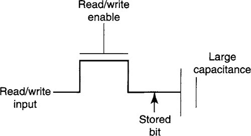
How can a bit be stored such that in the absence of writes and power failures, the bit stays indefinitely? Storing a bit as the output of the inverter shown in Figure A.3 will not work, because, left to itself, the output will discharge from a high to a low voltage via “parasitic” capacitances. A simple solution is to use. feedback: In the absence of a write, the inverter output can be fed back to the input and “refresh” the output. Of course, an inverter flips the input bit, and so the output must be inverted a second time in the feedback path to get the polarity right, as shown in Figure A.5. Rather than show the complete inverter (Figure A.3), a standard triangular icon is used to represent an inverter.
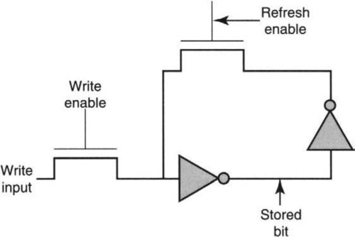
Input to the first transistor must be supplied by the write input when a write is enabled and by the feedback output when a write is disabled. This is accomplished by two more “pass” transistors. The pass transistor whose gate is labeled “Refresh Enable” is set to high when a write is disabled, while the pass transistor whose gate is labeled “Write Enable” is set to high when a write is enabled. In practice, refreshes and writes are done only at the periodic pulses of a systemwide signal called a clock. Figure A.5 is called a flip-flop.
A register is an ordered collection of flip-flops. For example, most modern processors (e.g., the Pentium series) have a collection of 32-or 64-bit on-chip registers. A 32-bit register contains 32 flip-flops, each storing a bit. Access from logic to a register on the same chip is extremely fast, say, 0.5–1 nsec. Access to a register off-chip is slightly slower because of the delay to drive larger off-chip loads.
STATIC RAM
A static random access memory (SRAM) contains N registers addressed by log N address bits A. SRAM is so named because the underlying flip-flops refresh themselves and so are “static.” Besides flip-flops, an SRAM needs a decoder that decodes A into a unary value used to select the right register. Accessing an SRAM on-chip is only slightly slower than accessing a register because of the added decode delay. At the time of writing, it was possible to obtain on-chip SRAMs with 0.5-nsec access times. Access times of of 1–2 nsec for on-chip SRAM and 5–10 nsec for off-chip SRAM are common. On-chip SRAM is limited to around 64 Mbits today.
DYNAMIC RAM
The SRAM bit cell of Figure A.5 requires at least five transistors. Thus SRAM is always less dense or more expensive than memory technology based on dynamic RAM (DRAM). In Figure A.6, a DRAM cell uses only a single transistor connected to an output capacitance. The transistor is only used to connect the write input to the output when the write enable signal on the gate is high. The output voltage is stored on the output capacitance, which is significantly larger than the gate capacitance; thus the charge leaks, but slowly. Loss due to leakage is fixed by refreshing the DRAM cell externally within a few milliseconds.
To obtain high densities, DRAMs use “pseudo-three-dimensional trench or stacked capacitors” [FPCe97]; together with the factor of 5–6 reduction in the number of transistors, a DRAM cell is roughly 16 times smaller than an SRAM cell [FPCe97].
The compact design of a DRAM cell has another important side effect: A DRAM cell requires higher latency to read or write than the SRAM cell of Figure A.5. Intuitively, if the SRAM cell of Figure A.5 is selected, the power supply quickly drives the output bit line to the appropriate threshold. On the other hand, the capacitor in Figure A.6 has to drive an output line of higher capacitance. The resulting small voltage swing of a DRAM bit line takes longer to sense reliably. In addition, DRAMs need extra delay for two-stage decoding and for refresh. DRAM refreshes are done automatically by the DRAM controller’s periodically enabling RAS for each row R, thereby refreshing all the bits in R.
A.2.5 Chip Design
Finally, it may be useful for networking readers to understand how chips for networking functions are designed.
After partitioning functions between chips, the box architect creates a design team for each chip and works with the team to create chip specification. For each block within a chip, logic designers write software register transfer level (RTL) descriptions using a hardware design language such as Verilog or VHDL. Block sizes are estimated and a crude floor plan of the chip is done in preparation for circuit design.
At this stage, there is a fork in the road. In synthesized design, the designer applies synthesis tools to the RTL code to generate hardware circuits. Synthesis speeds the design process but generally produces slower circuits than custom-designed circuits. If the synthesized circuit does not meet timing (e.g., 8 nsec for OC-768 routers), the designer redoes the synthesis after adding constraints and tweaking parameters. In custom design, on the other hand, the designer can design individual gates or drag-and-drop cells from a standard library. If the chip does not meet timing, the designer must change the design [SSH99]. Finally, the chip “tapes out,” and is manufactured, and the first yield is inspected.
Even at the highest level, it helps to understand the chip design process. For example, systemwide problems can be solved by repartitioning functions between chips. This is easy when the chip is being specified, is an irritant after RTL is written, and causes blood feuds after the chip has taped out. A second “spin” of a chip is something that any engineering manager would rather work around.
INTERCONNECTS, POWER, AND PACKAGING
Chips are connected using either point-to-high connections known as high-speed serial links, shared links known as buses, or parallel arrays of buses known as crossbar switches. Instead of using N2 point-to-point links to connect N chips, it is cheaper to use a shared bus. A bus is similar to any shared media network, such as an Ethernet, and requires an arbitration protocol often implemented (unlike an Ethernet) using a centralized arbiter. Once a sender has been selected in a time slot, other potential senders must not send any signals. Electrically, this is done by having transmitters use a tristate output device that can output a 0 or a 1 or be in a high-impedance state. In high-impedance state, there is no path through the device to either the power supply or ground. Thus the selected transmitter sends 0’s or 1’s, while the nonselected transmitters stay in high-impedance state.
Buses are limited today to around 20 Gb/sec. Thus many routers today use parallel buses in the form of crossbar switches (Chapter 13). A router can be built with a small number of chips, such as a link interface chip, a packet-forwarding chip, memory chips to store lookup state, a crossbar switch, and a queuing chip with associated DRAM memory for packet buffers.
A.3 SWITCHING THEORY
This section provides some more details about matching algorithms for Clos networks and the dazzling variety of interconnection networks.
A.3.1 Matching Algorithms for Clos Networks with k = n
A Clos network can be proved to be rearrangably nonblocking for k = n. The proof uses Hall’s theorem and the notion of perfect matchings. A bipartite graph is a special graph with two sets of nodes I and O; edges are only between a node in I and a node in O. A perfect matching is a subset E of edges in this graph such that every node in I is the endpoint of exactly one edge in E, and every node in O is also the endpoint of exactly one edge in E. A perfect match marries every man in I to every woman in O while respecting monogamy. Hall’s theorem states that a necessary and sufficient condition for a perfect matching is that every subset X of I of size d has at least d edges going to d distinct nodes in O.
To apply Hall’s theorem to prove the Clos network is nonblocking, we show that any arrangement of N inputs that wish to go to N different outputs can be connected via the Clos network. Use the following iterative algorithm. In each iteration, match input switches (set I) to output switches (set O) after ignoring the middle switches. Draw an edge between an input switch i and an output switch o if there is at least one input of i that wishes to send to an output directly reachable through o.
Using this definition of an edge, here is Claim 1: Every subset X of d input switches in I has edges to at least d output switches in O. Suppose Claim 1 were false. Then the total number of outputs desired by all inputs in X would be strictly less than nd (because each edge to an output switch can correspond to at most n outputs). But this cannot be so, because d input switches with n inputs each must require exactly nd outputs.
Claim 1 and Hall’s theorem can be used to conclude that there is a perfect matching between input switches and output switches. Perform this matching, after placing back exactly one middle switch M. This is possible because every middle switch has a link to every input switch and a link to every output switch. This allows routing one input link in every input switch to one output link in every switch. It also makes unavailable all the n links from each input switch to the middle switch M and all output links from M.
Thus the problem has been reduced from having to route n inputs on each input switch using n middle switches to having to route n – 1 inputs per input switch using n – 1 middle switches. Thus n iterations are sufficient to route all inputs to all outputs without causing resource conflicts that lead to blocking.
Thus a simple version of this algorithm would take n perfect matches; the best existing algorithm for perfect matching [HK73] takes O(N/n1.5) time. A faster approach is via edge coloring; each middle switch is assigned a color, and we color the edges of the demand multigraph between input switches and output switches so that no two edges coming out of a node have the same color.3 However, edge coloring can be done directly (without n iterations as before) in around O(N log N) time [CH82],
A.4 THE INTERCONNECTION NETWORK ZOO
There is a dazzling variety of (log N)-depth interconnection networks, all based on the same idea of using bits in the output address to steer to the appropriate portion, starting with the most significant bit. For example, one can construct the famous Butterfly network in a very similar way to the recursive construction of the Delta network of Figure 13.14. In the Delta network, all the inputs to the top (N/2)-size Delta network come from the 0 outputs of the first stage in order. Thus the 0 output of the first first-stage switch is the first input, the 0 output of the second switch is the second input, etc.
By contrast, in a Butterfly, the second input of the upper N/2 switch is the 0 output of the middle switch of the first stage (rather than the second switch of the first stage). The 0 output of the second switch is then the third input, while the 0 output of the switch following the middle switch gets the fourth input, etc. Thus the two halves are interleaved in the Butterfly but not in the Delta, forming a classic bowtie or butterfly pattern. However, even with this change it is still easy to see that the same principle is operative: outputs with MSB 0 go to the top half, while outputs with MSB 1 go to to the bottom.
Because the Butterfly can be created from the Delta by renumbering inputs and outputs, the two networks are said to be isomorphic. Butterflies were extremely popular in parallel computing [CSG99], gaining fame in the BBN Butterfly, though they seem to have lost ground to low-dimensional meshes (see Section 13.10) in recent machines.
There is also a small variant of the Butterfly, called the Banyan, that involves pairing the inputs even in the first stage in a more shuffled fashion (the first input pairs with the middle input, etc.) before following Butterfly connections to the second stage. Banyans enjoyed a brief resurgence in the network community when it was noticed that if the outputs for each input are in sorted order, then the Banyan can route without internal blocking. An important such switch was the Sunshine switch [Gea91]. Since sorting can be achieved using Batcher sorting networks [CLR90], these were called Batcher-Banyan networks. Perhaps because much the same effect can be obtained by randomization in a Benes or Clos network without the complexity of sorting, this approach has not found a niche commercially.
Finally, there is another popular network called the hypercube. The networks described so far use d-by-d building block switches, where d is a constant such as 2, independent of the size of N. By contrast, hypercubes use switches with log N links per switch. Each switch is assigned a binary address from 1 to N and is connected to all other switches that differ from it in exactly one bit. Thus, in a very similar fashion to traversing a Delta or a Butterfly, one can travel from input switch to an output switch by successively correcting the bits that are different between output and input addresses, in any order. Unfortunately, the log N link requirement is onerous for large N and can lead to an “impractical number of links per line card” [Sem02].