
4
Simple circuits
When it comes to teaching people how to read and draw schematic diagrams, two schools of thought prevail. One school feels that you should learn to read diagrams before you learn to draw anything. The other school feels that you should learn to read diagrams as part of the process of drawing them. Both sides of this issue have their merits, so let’s take advantage of them both! Certainly, you must start out by learning the basic component symbols. Then you should try to read as many schematic drawings as you can find. When this business starts to grow boring, you can draw your own simple diagrams. If you alternately read and draw schematics as the moods strike, you’ll get comfortable with them before long! I recommend that you devote half of your study time to reading and the other half to drawing.
Getting started
This chapter deals with reading and drawing diagrams of some simple electronic circuits shown in pictorial and schematic form. Using this method, you can actually see the physical layout for a device, and then see how the schematic representation derives from it. Some commercial schematics are produced in this manner. However, in most instances, a circuit is designed schematically first, and then built and tested from the schematic. If a circuit is experimental, some bugs will exist in the prototype, necessitating various component deletions, substitutions, or modifications. When these changes are made to the test circuit, the results are noted, and the schematic is changed accordingly. In the end, the finished and corrected schematic is a product of design theory, actual testing, and modification.
Figure 4-1 shows a simple circuit that everyone has used at one time or another. Basically, it’s a flashlight with the external case and the on/off switch removed. The device consists of a single electrochemical cell and an electric light bulb. This pictorial representation also shows the conductors, which attach to the light bulb and the battery. The conductors provide a current path between the battery and the light bulb.
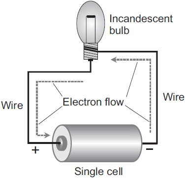
FIG. 4-1. Pictorial drawing of a flashlight circuit using a single electrochemical cell (or single-cell battery), some wire, and an incandescent bulb.
Follow the flow
In the circuit of Fig. 4-1, electrons travel from the negative terminal of the cell through the bulb element and back to the positive terminal of the cell, “leapfrogging” from atom to atom in the metal wire and the bulb filament. That’s how most electricians and engineers look at this situation. But some physicists will tell you that the current actually goes from the positive cell pole to the negative cell pole. That’s called theoretical current or conventional current.
In order to draw a schematic diagram of the flashlight drawn in Fig. 4-1, you need to know three schematic symbols. These represent the electrochemical cell, the conductors, and the bulb, as shown in Fig. 4-2. Once you know the symbols, you can assemble them in a logical manner based on the appearance of the circuit in the pictorial drawing.
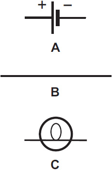
FIG. 4-2. Schematic symbols for an electrochemical cell (A), an electrical conductor such as wire (B), and an incandescent bulb (C).
Start by drawing the cell symbol. You can think of the cell as the heart of the circuit because it supplies all of the power for the device; it “pumps the electrons” through everything! Next comes the symbol for the light bulb, which you can draw at any point near the cell. Using this example, you should try to make the schematic symbols fall in line with the way the pictorial diagram appears. This layout places the light bulb above the cell.
Now that you’ve drawn the two major symbols, you can use the conductor symbols (plain, straight, solid, black lines) to hook them together. Notice that the pictorial drawing shows two conductors. Therefore, the schematic diagram also has two conductors. Figure 4-3 shows the completed schematic drawing, which is the symbolic equivalent of Fig. 4-1.
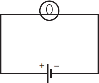
Figure 4-3 is by no means the only way that you can represent this simple circuit in schematic form. But any schematic representation will require the use of the same three basic symbols: cell, bulb, and conductors. The only changes that can occur involve the positioning of the component symbols on the page. Figure 4-4 shows two different alternatives for portraying the same circuit. All three of these diagrams (the one in Fig. 4-3 and the two in Fig. 4-4) are electrically equivalent, but they look somewhat different as a result of the relative positions of the components on the page.
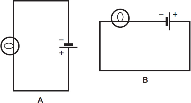
FIG. 4-4. Alternative arrangements for the flashlight schematic. At A, cell and bulb “vertical;” at B, cell and bulb both on top.
Let’s change this circuit a little bit, in order to gain proficiency in reading and writing schematics. Figure 4-5 shows the same basic flashlight circuit, but an additional cell and a switch have been added. This configuration is quite common for flashlights sold in the United States. By examining this pictorial drawing, you can see that any schematic representation will need symbols for the cells, the conductors, the light bulb, and the switch. Figure 4-6 shows the symbols that you’ll need to produce an accurate and complete schematic drawing of this circuit. Again, you should draw the symbols in the same basic order as the components are wired in the circuit. Figure 4-7 shows the resulting schematic. Note that the two cell symbols are drawn separately, connected in series, with polarity markings provided for each one. In the series connection, the positive terminal of one cell goes to the negative terminal of the other. The same two conductors are used from the cell terminals, but you need a third one to connect the switch to the light bulb, and you might also need a fourth one to connect the two cells together to form a battery (unless the cells rest directly against each other, a common state of affairs inside commercially manufactured flashlights). Figure 4-7 shows the switch in the off position.
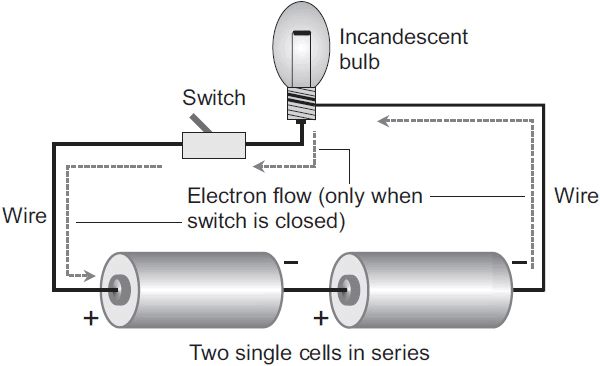
FIG. 4-5. Pictorial drawing of a flashlight circuit using two single cells in series, some wire, a switch, and an incandescent bulb.
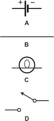
FIG. 4-6. Symbols for components in the two-cell switched flashlight: Cell (A), wire (B), bulb (C), and switch (D).
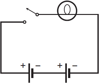
Now you know what a common two-cell flashlight looks like when represented with schematic symbology. The next time that you switch one of those things on, you can imagine the switch symbol in Fig. 4-7 moving from the off (or open) position to the on (or closed) position.
Figure 4-8 is a pictorial representation of a device called a field-strength meter. Wireless communications engineers sometimes use this type of meter to see whether or not an RF electromagnetic (EM) field exists at a given location. You’ll find this little circuit quite handy if you enjoy amateur radio, or if you need to locate the source of something that’s causing RF interference. The circuit consists of an antenna, an RF diode, a microammeter (a sensitive current meter graduated in millionths of an ampere), and a coil. In order to draw this circuit schematically, you need to know the symbols for an antenna, a coil, a microammeter, and a diode, all of which appear in Fig. 4-9. Using the same method as before, you can draw the schematic by connecting the symbols in the same geometric sequence as the components they represent appear in the circuit.
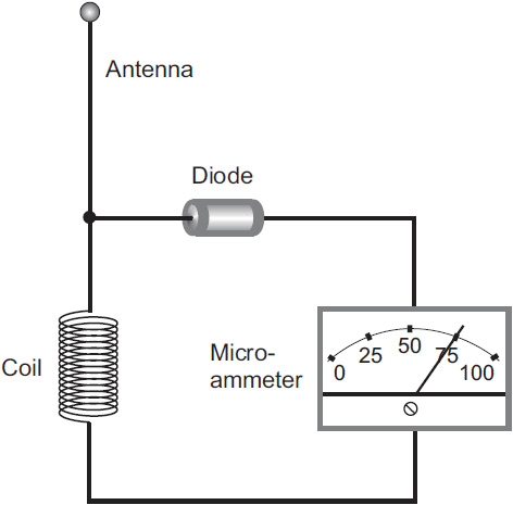
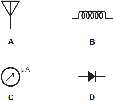
FIG. 4-9. Schematic symbols for the components in the field-strength meter: Antenna (A), coil (B), microammeter (C), and diode (D).
Figure 4-10 is a schematic of the field-strength meter shown pictorially in Fig. 4-8. This drawing involves nothing more than substitution of the schematic symbols for the pictorial symbols. As before, the parts need not be physically placed in the same positions as the schematic diagram suggests, but they must be interconnected precisely as indicated in the schematic. When you build a circuit from a schematic diagram that you trust, you should double-check and triple-check your actual component interconnections to make sure that they agree with the schematic. If you try to build the circuit shown in Fig. 4-10 and make a mistake in the wiring connections, you cannot expect it to work. In more sophisticated devices and systems, wiring mistakes can cause component damage and, once in awhile, give rise to dangerous situations!
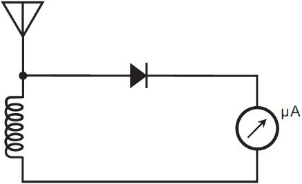
In the circuit of Figs. 4-8 and 4-10, an EM field induces an RF current in the antenna and coil. That current is high-frequency AC. The diode rectifies the AC wave by “chopping off” either the positive half or the negative half of every cycle (depending on the diode’s polarity) to produce pulsating DC like the output of a simple rectifier. The microammeter registers this current. As the strength of the EM field increases, the current increases, and the meter reading goes up.
Previously, we compared schematic drawings to road maps. A road map is supposed to indicate exactly what a motorist will experience in practice. The schematic drawing does the same thing. The highway lines that interconnect towns on a map correspond to the conductor lines that interconnect components in a schematic. A road map shows the route that a motorist takes while driving from town to town on the earth’s surface, whereas a schematic diagram shows the route that a current or signal takes through the components in an electronic circuit.
Now let’s look at something that’s a little more complicated. Figure 4-11 is a schematic diagram of a power supply that produces pure, battery-like DC from utility AC. As you read this diagram from left to right, you’ll see that a power plug goes to the transformer primary winding (the one to the left of the pair of vertical lines) through a fuse. At the top of the transformer secondary winding (the one on the right), a rectifier diode is connected in series. Following the diode, an electrolytic capacitor (note the polarity sign) is connected between the output of the rectifier and the bottom of the transformer secondary. A fixed resistor is connected in parallel with the capacitor. The DC output appears at the extreme right.
The physical size and weight of a real-world power supply, which you can build on the basis of Fig. 4-11, will depend on the voltage and current that you need to get from it. Because DC power supplies have polarized outputs, positive and negative signs indicate the output voltage polarity. Any power supply that uses a single diode, capacitor, and resistor will have this same basic configuration. Whether the output is 5 V at 1 A or 5000 V at 50 A, the schematic drawing will look the same. Figure 4-11 says nothing about how many volts or amperes the transformer, diode, capacitor, and resistor are meant to handle. You could add special features, such as a voltage regulator, overcurrent protector, voltmeter, or ammeter to your circuit and insert the symbols at the proper points in the schematic; but all half-wave DC power supplies are built around “cores” whose diagrams look like Fig. 4-11.
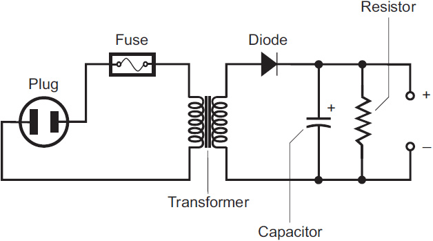
In the circuit of Fig. 4-11, utility AC appears at the plug on the left. The AC travels through the fuse and flows in the transformer primary. In the secondary, AC also flows, but the voltage across the transformer secondary might be higher or lower than the voltage across the primary (depending on the transformer specifications). The diode allows current to flow only one way; in this case the electrons can go only from right to left (against the arrow). As a result, pulsating DC comes out of the diode. The capacitor gets rid of the pulsations, called ripple, on the DC output from the diode. The resistor discharges, or bleeds, the capacitor when you unplug the whole device from the utility outlet.
Component labeling
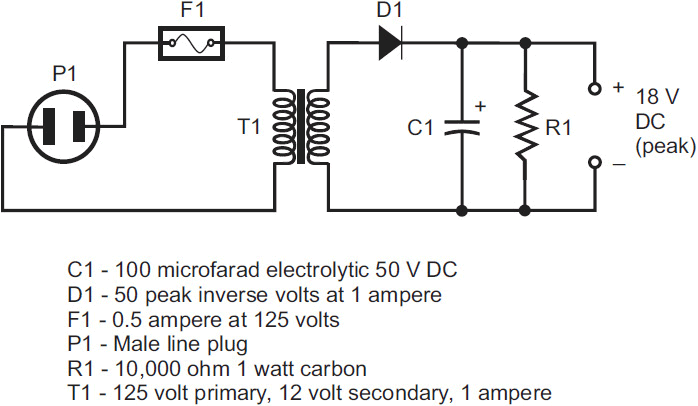
Figure 4-12 is a schematic of the same circuit as the one shown in Fig. 4-11, but in this case, each component has an alphabetic/numeric designation. These designators all refer to a components list at the bottom. Now you can see that this power supply uses a transformer with a primary winding rated at 125 V and a secondary winding that yields 12 V. The circuit has a diode rated at 50 peak inverse volts (PIV) and a forward current of 1 A; a 100-microfarad, 50-V capacitor; and a 10,000-ohm, 1-W carbon resistor. The fuse is rated at 0.5 A and 125 V.
The letters that identify each component are more or less standard. Notice that each letter is followed by the number 1. The designation T1, for instance, indicates that the component is a transformer (T) and that it’s the first such component referenced. If this circuit had two transformers, then one of them would bear the label T1 and the other one would bear the label T2. The numbers reference the position or order on the components list; they serve no other purpose. The diode carries the reference designator D1, with D serving as the standard abbreviation for most diodes. Standardization is not universal, though! In some instances, the diode might bear the label SR1, where the letters SR stand for silicon rectifier. Some Zener diodes are labeled as ZD1, ZD2, and so on. This labeling makes little difference as long as you write the component designations next to the corresponding symbols. If you replaced the designation D1 with SR1, your readers would still know that the abbreviation went with the symbol for the diode, as long as you made sure to put the abbreviation close enough to the symbol.
In the situation of Fig. 4-12, you don’t have to include a number next to each component designation because only one of each component is used to make up the entire schematic! You could simply write P for the plug, F for the fuse, T for the transformer, D for the diode, C for the capacitor, and R for the resistor. Or, if you had confidence that your readers knew all the symbols, you could leave out designators altogether! Nevertheless, standard diagramming practice requires that you always include a letter and a number, even if only one of a certain component type exists in the whole circuit.
In complicated electronic systems, several hundred components of the same type (resistors, for example) might exist, many of which come from the same family. For instance, if you see the designation R101, then you know that the system contains at least 101 resistors. If you want to know the type and value of resistor R101, you will have to look up R101 in the components list to find its specifications.
Tip
You can use the schematic of Fig. 4-12 to build a power supply with a peak output of about 18 V DC. But before each component was referenced, the schematic had no practical use. Figure 4-11 illustrates a generic half-wave power supply, but that schematic doesn’t give you any practical information other than the relative arrangement of the components.
Table 4-1 shows the standard letter designations for most types of electronic components that you’ll encounter in schematic diagrams. Some of these designations can vary in real-world documentation, depending upon the idiosyncrasies of the person making the drawing or designing the circuit. You should find it easy to memorize (yes, that’s right, memorize!) the information in Table 4-1 because most of the designations merely comprise the first letters of the component names. If the component has a complex name, such as silicon-controlled rectifier, the first letters from each of the three words is used, so you get SCR1. A resistor is designated by R, a capacitor by C, a fuse by F, and so on. Conflicts do arise, of course. If you want to designate a relay, you need to use some letter other than R because R indicates a resistor! The same thing happens if you want to label a crystal; you can’t use C because that letter refers to a capacitor. Look through Table 4-1 from time to time as you read and draw schematic diagrams, and eventually you’ll absorb all the information in there.
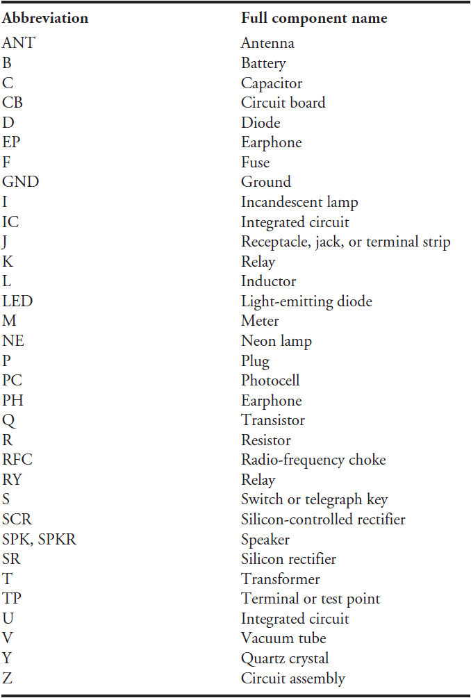
The circuit of Fig. 4-13 has a full-wave bridge rectifier along with a better ripple filter than the simple capacitor used in the previous power supply. The inductor, L1, is a filter choke, which, along with capacitor C1, does an excellent job of “smoothing” out the DC so it resembles what comes from a 12-V battery (pure DC with no ripple).
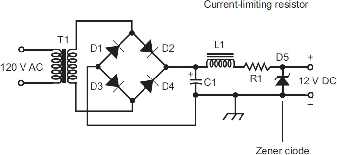
FIG. 4-13. A power supply that uses full-wave bridge rectification (four rectifier diodes) and Zener-diode voltage regulation.
Figure 4-14 shows a voltage-doubler power supply. The two capacitors, C1 and C2, charge up from the full transformer secondary output after the current goes through diodes D1 and D2. Because the two capacitors are connected in series, they act like two batteries in series, giving you twice the voltage. But there’s a catch! A voltage doubler power supply works well only at low current levels. If you try to draw too much current from one of these power supplies, you’ll “draw down” the capacitors and the voltage will decrease.
In Figs. 4-13 and 4-14, the letter designations are the same for each component type, but the numbers advance, one by one, up to the total number of units. So, for example, in Fig. 4-13 you see diodes D1 through D5 because the circuit contains five diodes. (The Zener diode to the right of R1 has the letter D just like the rectifier diodes have, but you can tell it’s a Zener diode because of the bent line in the symbol.) All the other components have only one of each type. In Fig. 4-14, you see two diodes, two capacitors, and two resistors, so the numbers for D, C, and R go up to 2. The transformer is all alone, so you see only the number 1 following the letter T.
Even though multiple components might all have the same value (820 ohms, for example, or 50 microfarads), they must nevertheless get separate numerical designations when two or more of them exist in a single circuit.
Schematics don’t reveal every physical detail of a device, the way a photograph or detailed pictorial would do. Schematics depict schemes, that’s all! The schematic diagram for a device allows engineers and technicians to make the correct electrical connections when putting it together, and to locate the various components when testing, adjusting, debugging, or troubleshooting it. If you find all this talk overly philosophical, maybe a real-world example will clear things up. Remember that solid lines in schematic drawings represent conductors. However, a conductor doesn’t have to be a length of wire. It might be part of a component lead, or perhaps a foil run on a printed circuit board (the latter-day equivalent of a connecting wire). Whether or not a separate length of wire is needed to interconnect two components will depend on how close together those components are in the physical layout.
Examine the simple schematic of Fig. 4-15. The circuit contains three resistors, all of which go together in a parallel arrangement. Taking the schematic literally, a conductor connects the left-hand side of R1 to the left-hand side of R2. Another conductor goes between the left-hand side of R2 and the left-hand side of R3. Two other conductors connect the right-hand sides of the components. In practice, the connections might be made with wires attached to the resistor leads, but if the components are close enough together, the leads themselves can form the interconnections. Then Fig. 4-15 will represent the physical arrangement shown in Fig. 4-16.
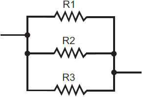
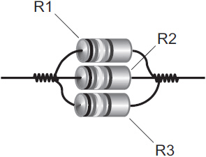
Naturally, if you want to follow good engineering principles, you’ll want to make all of your electronic circuits as compact (and dependable) as possible by using a minimum amount of point-to-point wiring and trying to make the component leads serve for interconnection purposes whenever you can. Of course, in the above example, if the three resistors had to go in different parts of the circuit separated by some physical distance, then you would need to use interconnecting conductors between them. However, as you design the physical layout of a circuit, you should try to minimize the overall length (that is, the total length) of all the interconnecting wires or foil runs combined.
Troubleshooting with schematics
Engineers and technicians use schematic diagrams to create electronic devices, but these diagrams can also prove invaluable for troubleshooting equipment when problems develop. Knowing how to read schematic diagrams, however, is not enough. You also need to know what tasks the various components actually perform, as well as how the diverse circuits work together in a complete system. No matter how proficient you might get at electronics troubleshooting, seemingly simple repair jobs can explode into major headaches without complete, accurate, and clear schematic representations of the hardware.
Remember!
Schematic diagrams clarify circuits. They present the circuit elements in a logical and easy-to-understand manner. They tell you very little, if anything, about the component layouts in actual devices.
When you build a circuit from a schematic drawing, the physical object rarely bears much physical resemblance to the schematic. It’s impractical to build a complex electronic circuit by placing the components in the exact same geometrical relationship as they appear in the schematic. The diagrams purposely spread out the components on the page for easy reading. Schematic diagrams are two-dimensional, whereas real-world electronic components are three-dimensional. You need only to look inside of a major electronic device, such as a television set or computer, to realize the complexities that you’d face in troubleshooting a complex system without the help of a schematic diagram.
If you know a fair amount about electronic components and how they operate in various circuits, then you can use a schematic diagram to get a good idea (without any equipment testing) where a particular problem might occur. Then, by testing various circuit parameters at these critical points and comparing your findings with what the schematic diagram indicates should be present, you can make a quick assessment of the trouble. For example, if a schematic diagram shows a direct connection between two components in a circuit, and a check with an ohmmeter reveals a high resistance between the two, then you can assume that a conductor is broken or a contact has been shaken loose. If a schematic diagram shows only a capacitor between two components (with no other circuit routes around it) and a reading with your ohmmeter shows zero ohms or only a couple of ohms, you can assume that the capacitor has shorted out and you’ll have to replace it.
Beginners to electronics troubleshooting and diagram reading sometimes assume that a professional can instantly isolate a problem to the component level by looking at the schematic. This idealized state of affairs might prevail for a few simple circuits, but in complex designs the situation grows a lot more involved. Often, the schematic diagram allows a technician to make educated guesses as to where or what the trouble might be, but an exhaustive diagnosis will nearly always require testing. A particular malfunction in an electronic device will not necessarily have a single, easy-to-identify cause. Often there are many possible causes, and the technician must whittle the situation down to a single cause by following a process of elimination.
Suppose that a circuit will not activate, and no voltage can be detected through testing at any contact point indicated by the schematic. Chances are good that no current is passing through the circuit at all. However, you don’t know from this observation exactly what has caused the failure. Has one of the components in the power supply become defective? Has the line cord been accidentally pulled from the wall outlet? Has a conductor broken between the output of the power supply and the input to the electronic device? Has the fuse blown?
In a scenario of this sort, you will almost certainly want to consult the schematic diagram as you go through all of the standard test procedures. You might wish to find the contact point that serves as the power supply output, indicated on the schematic. If you test the voltage at this point and it appears normal, then you can assume that the problem lies somewhere further along in the circuit. The schematic diagram and the test instrument readings allow you to methodically search out and isolate the problem by starting at a point in the circuit where operation is normal and proceeding forward until you get to the point where the circuit shows some abnormality.
Continuing with the same example, if no output comes from the power supply, you know that you must search backward toward the trouble point. You will continue testing until you reach a point of normal operation and then proceed from there. Using a schematic diagram, you’ll follow your progress and thereby narrow the problem area down to something between two points (the point farthest back from the output at which the problem exists, and the point furthest forward from the input where things test normal). Chances are good that this narrowing process will isolate the trouble to a single component or circuit connection.
You could follow all of the foregoing steps without a schematic diagram, although it would take you a lot longer to do it, and it would increase the risk of your making a mistake. As you become more experienced in the art of electronics troubleshooting, the information contained in schematic drawings becomes increasingly valuable.
Go back and look again at the flashlight circuit of Fig. 4-7. Although the schematic diagram does not say so, the two batteries in series should yield a DC potential of 3 V because a typical flashlight cell provides 1.5 V, and DC voltages add up in series connections. Some schematic diagrams provide voltage test points and maximum/minimum readings that you should expect, but this simple example doesn’t.
Suppose that the flashlight has stopped working, and you decide to test the circuit with a volt-ohm-milliammeter (VOM), also called a multimeter, with the help of Fig. 4-7. First of all, you can measure the individual voltages across the cells. With the meter’s positive probe placed at the positive cell terminal and the negative probe at the negative terminal, you should get a reading of 1.5 volts across each cell. If both read zero, then you know that both cells have lost all their electrical charge. If one cell reads normal and the other one reads zero, then in theory you should only have to replace the one that reads zero. (In practice, it’s a good idea to replace entire sets of cells all at once, even if some of them still test okay). If both cells read normal, then you can test the voltage across the bulb. Here, you should expect a reading of 3 V under normal operation with the switch closed. If you do indeed observe 3 V here, then you can diagnose the problem by looking at the schematic. The bulb must have burned out! The schematic shows you that current must go through the light bulb if the bulb can conduct, so it must light up. If voltage is available at the base of the light bulb, then current will flow through the element unless it has opened up. But of course, if the bulb filament has broken apart, no current can flow through the bulb, so it won’t light up. In fact, with a burned-out bulb, no current will flow anywhere at all in the circuit.
On the other hand, let’s say that you get a normal reading at the batteries, but no reading whatsoever at the light bulb. Obviously, a break must exist in the circuit between these two circuit points. Three conductors are involved here: one between the negative terminal of the battery and one side of the bulb, another between the positive battery terminal and the switch, and another between the switch and the other side of the bulb. Obviously, one of the conductors has broken (or a contact has been lost where the conductor attaches to the battery), or maybe the switch is defective. While you keep an eye on the schematic, you can test for a defective switch by placing the negative meter probe on the negative battery terminal and the positive probe on the input to the switch. If you see a normal voltage reading, then the switch must be defective. If you still get no voltage reading, then one of the conductors has come loose or broken.
Admittedly, the scenario just described presents only a basic example of troubleshooting using a schematic diagram—almost as simple as things can get! But imagine that the flashlight circuit is highly complex, one you know nothing about. Then the schematic diagram becomes an invaluable aid and a necessary adjunct to the standard test procedures with the VOM. This same basic test procedure will be used over and over again when testing highly complex electronic circuits of a similar nature. In most instances, no matter how complicated the circuit design looks, it’s actually a combination of many simple circuits. But if you have to do a comprehensive troubleshooting operation, you might have to test each and every one of those circuits individually.
A more complex circuit
Figure 4-17 shows a diagram for a somewhat more complicated, real-world electronic circuit presented in a form intended to assist a troubleshooting technician. The circuit has a single NPN bipolar transistor along with some resistors and capacitors. Note that test points (abbreviated TP) exist at three different locations: TP1 at the emitter of the transistor, TP2 at the base of the transistor, and TP3 at the collector of the transistor. If you need to troubleshoot this circuit (which happens to be a low-power amplifier of the sort you might find in a vintage radio receiver or hi-fi set), you’ll connect your VOM between chassis ground and each one of these three points, in turn. You’ll carefully note the meter readings and compare them with known normal values.
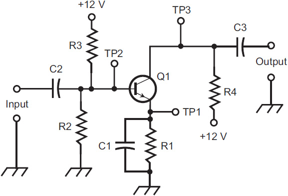
FIG. 4-17. Schematic diagram of an amplifier circuit that includes component designators and three test point (TP) locations.
The circuit of Fig. 4-17 receives a weak input AC signal (such as the output of an ultrasonic pickup) and boosts it so that it can drive a device that consumes significant power (such as a switching circuit). The general signal flow goes from left to right. The original AC signal enters at the input terminals, passes through capacitor C2, and reaches the base (left-hand electrode) of transistor Q1. The base acts as an adjustable “current valve” that causes large current fluctuations through Q1 as the electrons flow from ground through R1 to the emitter (the bottom electrode), then onward to the collector (top electrode), and out through R4 to the positive power supply terminal. Capacitors C2 and C3 allow the AC signals to pass while blocking DC from the power supply so that the DC won’t upset the operation of external circuits. Capacitor C1 keeps the transistor’s emitter at a constant DC voltage while allowing the input signal to enter unimpeded. The resistors R2 and R3 have values carefully chosen to place precisely the right DC voltage, called bias, on the base of Q1, ensuring that the transistor will work as well as it possibly can in this application.
In many electronic circuits, actual voltages can deviate from design values by up to 20 percent; if this information is important, you’ll usually find the error range at the bottom of the schematic drawing or in the accompanying literature. If the readings obtained are within this known error range (called the component tolerance), then you can tentatively assume that this part of the circuit is working properly. However, if the readings obtained are zero or well outside of the tolerance range, then you have pretty good reason to suspect a problem with the associated circuit portion, or possibly with other circuits that feed it.
Many schematic drawings that accompany electronic equipment, especially “projects” that you build from a kit containing individual components, include information that aids not only in troubleshooting, but also in the initial testing and alignment procedures that you must follow as soon as you’ve completed the physical assembly process. As a further aid, the literature might include pictorial diagrams that show you where each part belongs on the circuit board or chassis. That way, you can follow the circuit not only according to its electrical details, but along the physical pathways as they actually look.
According to standard schematic drawing practice, every component should bear a unique alphabetic/numeric label to designate it, as you see in Fig. 4-17. However, a few alternative labeling forms are also acceptable. Figure 4-18 shows the same circuit as the one in Fig. 4-17, but the parts list has been eliminated and the diagram contains no alphabetic/numeric designations. Instead, the components are identified only by their schematic symbols along with value designations or industry standard part designations. Using the example shown, we know that the transistor is a 2N2222 type, and that the resistors have values of 470, 33k (33,000), 330k (330,000), and 680 ohms. The input capacitor has a value of 0.01 microfarad (μF) and the output capacitor has a value of 0.1 μF. The emitter capacitor, which goes across the 470-ohm resistor, has a value of 4.7 μF.
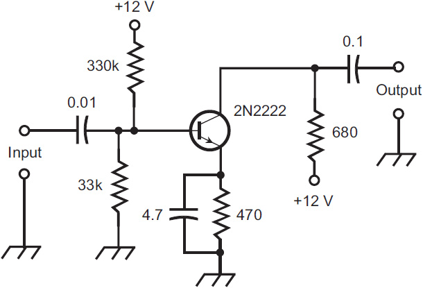
FIG. 4-18. Schematic diagram of the amplifier circuit from Fig. 4-17, but with component values instead of sequential designators. All capacitances are in microfarads (μF). All resistances are in ohms (Ω); k = 1000.
In situations like the one in Fig. 4-18, you’ll usually see a statement at the bottom of a schematic diagram that includes information about the units for the value designations. Such a statement might read “All capacitors are rated in microfarads (μF). All resistances are given in ohms (Ω), where k = 1000 and M = 1,000,000.”
Schematic/block combinations
Once in awhile, you’ll encounter a “hybrid” drawing that consists of a block diagram and a schematic diagram combined. Figure 4-19 shows an example of this approach, which works well when you want to highlight and explain a particular circuit, and to clarify its relationship to other circuits in a system. The detailed schematic portion of Fig. 4-19 shows a buffer amplifier of the sort you’ll find in a radio transmitter. An oscillator (which precedes the buffer) and an amplifier (which follows the buffer) are represented as blocks with labels inside.
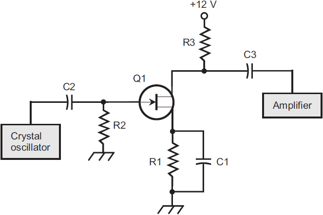
FIG. 4-19. A combination block/schematic diagram of an oscillator, buffer, and amplifier system, showing the schematic details of the buffer portion.
This diagram serves two purposes. First, as you read the schematic portion, you can study the actual component makeup of the buffer circuit. Second, you get a good idea as to the buffer’s place in the overall system relative to the other circuits. The block/schematic representation in Fig. 4-19 clearly shows you that the buffer receives its input from a crystal-controlled oscillator, and also that the buffer sends its output to an amplifier. Another schematic diagram and block diagram combination might describe another portion of this same device, which you might recognize as a simple radio transmitter.
Figure 4-20 is a schematic/block “hybrid” diagram in which the oscillator is portrayed in schematic detail, but the buffer and the amplifier are represented only as blocks. This figure tells you that the oscillator output goes to the buffer, which then sends the signal along to the amplifier. The only new information obtained here is contained in the schematic representation of the oscillator. If you look at Figs. 4-19 and 4-20 together, however, you can picture in your mind a diagram in which all of the system’s detail is included up to the point where the signal enters the amplifier. The oscillator portion of Fig. 4-20 also tells you that the oscillator is designed to generate Morse code signals because it contains a telegraph key!
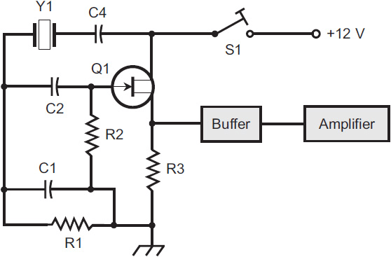
FIG. 4-20. A block/schematic diagram of the system from Fig. 4-19, showing the schematic details of the oscillator portion.
Now let’s “shift gears” and recall the block diagram of the AC-to-DC converter that you saw all the way back in Fig. 2-1. Figure 4-21 shows the schematic representation of that device, along with a duplicate of Fig. 2-1 to save you the trouble of having to flip pages. As you compare the two diagrams, note that in the schematic (at A), all of the actual components are shown, rather than merely portraying the stages as labeled blocks (at B). Figure 4-22 is a more comprehensive diagram that shows how the block diagram of this same device relates to the schematic diagram, while revealing all of the details originally present in both diagrams.
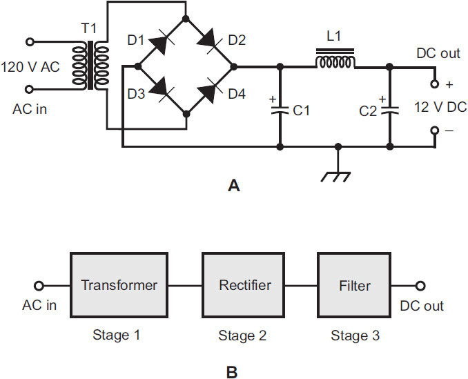
FIG. 4-21. Schematic diagram of an AC-to-DC converter (at A), such as the one portrayed in the block diagram all the way back in Fig. 2-1 (reproduced here at B).
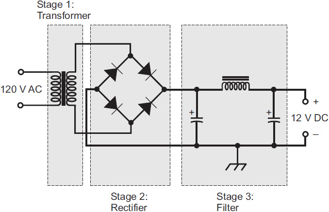
FIG. 4-22. Here’s how the block diagram of Fig. 2-1 relates to the schematic diagram of Fig. 4-21. (Component designators have been omitted to avoid clutter.)
To briefly explain the AC-to-DC converter circuit, more commonly called a power supply, the input electricity enters at the extreme left-hand end of all versions of the diagram (Figs. 4-21 and 4-22). The AC goes to the transformer to set up the proper ratio for conversion to DC. The four diodes in the diamond configuration constitute the rectifier, which converts the AC to pulsating DC, making use of both halves of the cycle. The final stage, the ripple filter, acts to smooth out the pulsations in the DC after the conversion. The “smoothed-out” or “pure” DC then goes along to the output terminals at the right-hand end, where it appears as a voltage just like the electricity that you’d find at the terminals of a 12-V battery.
Summary
This chapter has provided a brief sampling of simple electronic circuits, showing how you can read diagrams to learn how circuits are put together, or draw diagrams on the basis of known circuit details. After a bit more training, you should be able to view a simple schematic and easily visualize what the finished circuit will look like, maybe even getting an idea of how you might go about arranging the components on a circuit board (even though the schematics or block diagrams don’t explicitly tell you what to do in that respect).
You know that a roadway, as you drive along it in your car, does not look like the line that represents it on a map. You can visualize a secondary road or even a superhighway and do so whenever you see their symbols (although there’s nothing like traveling along a road in both directions to learn all about it). The same principle holds true when reading schematic diagrams. When you see a bunch of schematic symbols in a diagram, you can visualize the component interconnections and perhaps make a few mental notes on the physical aspects of the circuit construction (although there’s nothing like looking at, and using, a finished electronic device). Schematic symbology will become a new language for you—one in which you will eventually learn to think, just as you can think in terms of words, mathematical equations, musical scores, architectural blueprints, Morse code, or any other language.