

246 Computer Architecture and Organization
bits of Port C form group B. Group A is programmable to function in any one of three possible modes,
Mode 0, mode 1 and mode 2. Group B is programmable to work in any one of two possible modes,
mode 0 and mode 1. mode 0 is basic I/O mode, mode 1 is strobed I/O mode and mode 2 is bidirectional
data bus mode.
In Mode 0, the basic I/O mode, eight bits of port A, eight bits of port B, lower four bits of port C and
upper four bits of port C may be independently programmed as either input or output. If programmed
to act as output port, the output data, written by the processor within the port register, is latched . This is
the reason behind the faster response of a processor, in case of programmed output, as we have already
indicated in the last section. However, input data in case of mode 0, is not latched and must be stable at
the time of reading by the processor.
To summarize, mode 0 of 8255 is an example of programmed I/O and offers a simpler mode of input
as well as output, where output operation is faster and completion of the input operation is dependent
upon the external source, which is sending the data to the processor through the input port of 8255.
8.6 INTERRUPT DRIVEN I/O
Mode 1 and mode 2 of 8255 PPI are example cases of interrupt driven I/O. In mode 1 both port A and
port B may act as either interrupt driven input or interrupt driven output. In the case of mode 0 (basic
input–output mode), we have observed that input data are not latched. This drawback forces the proces-
sor to keep on reading the input port till the data are received. This de ciency is eliminated in mode 1.
We shall discuss about the input case rst and then take up the output case of mode 1 of data transfer,
using 8255.
8.6.1 Strobed Input Mode
When programmed to function in mode 1, the input data may be latched in port A or port B by a strobing
signal from the external device sending the data. This is explained through Figure 8.8, assuming port
A is programmed to function in strobbed input mode. Note that all eight pins of port A act as input, to
receive data from external device. In this case [ Figure 8.8 (a)], PC4 would accept a strobe signal from
Figure 8.8 Port A of 8255 PPI in strobed input mode (a) Interfacing signals
(b) Timing diagram
M08_GHOS1557_01_SE_C08.indd 246M08_GHOS1557_01_SE_C08.indd 246 4/29/11 5:14 PM4/29/11 5:14 PM

Input / Output Organization 247
the external device and PC5 would send an acknowledgement signal (IBF or Input Buffer Full) to the
external device. PC3 acts as an interrupt signal generating pin, which may be used to draw the attention
of the CPU when data is received. It is this feature, which is unique for all cases of interrupt driven I/O,
releasing the processor from the burden of continuously watching the input port, as we have noted for
mode 0 of 8255 in Section 8.5.
Through the timing diagram presented in Figure 8.8 (b), we may observe that the data (say 7AH)
along with a strobing signal (STB, active low) is sent by external device to 8255. Whenever this
strobe signal goes low, it indicates 8255 that the external device has sent some data through port A. To
acknowledge this new situation, 8255 makes it IBF output high, which informs the external device that
8255 has received the data (acknowledgement). After IBF goes high, the external device restores the
original status of STB signal and this rising edge of STB automatically latches the data in port A to the
internal latch of 8255. This change in STB signal (from low to high) triggers the interrupt output from
8255 through its PC3 pin by making it high. It is expected that this interrupt generating signal from PC3
is connected with the processor either directly or through an interrupt controller (e.g., 8259, which we
shall discuss shortly).
The processor, after receiving the interrupt, branches to the corresponding interrupt service routine,
which is expected to read the data from port A of 8255. Therefore, the RD signal goes low during this
reading operation which, in turn, withdraws the interrupting signal originated by PC3, making it low
again. After completing the reading operation and receiving the data (7AH) through D0 – D7, the pro-
cessor makes RD high, which forces the IBF output (from PC5 of 8255) low, indicating the external
device that 8255 port A is now free again to accept another fresh byte of data if required.
At this stage, it is suggested that the reader should stop proceeding further and take a stock
of the situation. Whatever described just now forms a very important concept of computer
architecture. First, note that the whole process of strobed input is completely automatic and
initiated exclusively by the input device. Second, every step of this process is dependent upon
its previous step and if the previous step remains incomplete, the entire process would wait
till the completion of that previous step (a very very important feature). Third, the entire
procedure is so much logically dependent upon each other that nothing would go wrong. The
reader may spend some additional time to further study the timing diagram presented in
Figure 8.8 (b) and verify each and every statement of this paragraph.
F
O
O
D
F
O
R
T
H
O
U
G
H
T
8.6.2 Strobed Output Mode
Although the methodology is identical, there are some minor differences between a strobed input and
strobed output for 8255, working in mode 1. Assuming again the case of port A, the interfacing signals
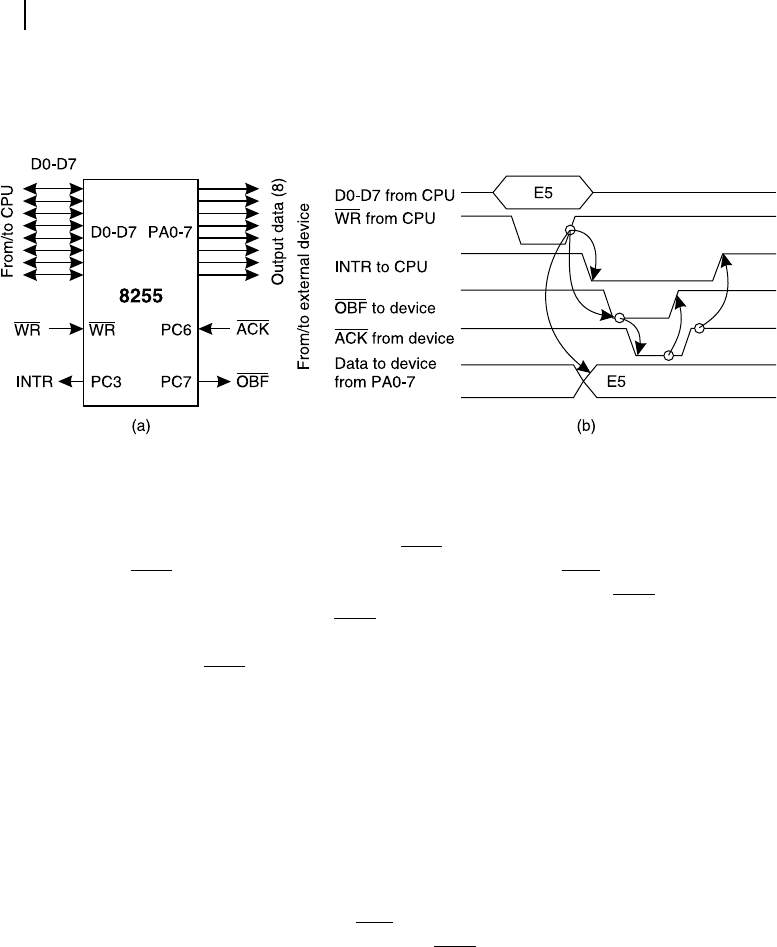
and the timing diagram for strobed output are shown in Figure 8.9 .
In this case, the data transmission to an external device starts with the interrupting signal. After
receiving the interrupt, processor writes the outgoing data (say E5H) to port A through its data lines
(D0 – D7) and activating the WR signal. After completion of writing, WR goes from low to high, which
M08_GHOS1557_01_SE_C08.indd 247M08_GHOS1557_01_SE_C08.indd 247 4/29/11 5:15 PM4/29/11 5:15 PM
248 Computer Architecture and Organization
produces three distinguished effects. First, the output data (E5H) is available through port A. Second,
INTR (through PC3) goes low, withdrawing the interrupt to the processor. Third, it triggers OBF output
from 8255 low, indicating the external device that a valid data is available through port A.
Figure 8.9 Port A of 8255 PPI in strobed output mode (a) Interfacing signals
(b) Timing diagram
The external device, sensing OBF to be low, lowers ACK for acknowledgement and reads the data from
port A. The low in ACK indicates 8255 that now it is time to bring back OBF to its original high state,
as the data is acknowledged by the external device. After completion of reading, ACK is brought to high
indicating completion of reading. This high in ACK triggers the INTR from 8255 to generate another inter-
rupting signal to the processor to repeat the whole process again. The receiving device may also initiate the
whole process by making its ACK signal from low to high and thus triggering the INTR to the processor.
8.6.3 Bidirectional Data Transfer Mode
Communication in this strobed input or strobed output mode of 8255 serves the basic purpose of inter-
rupt driven data transfer. However, if the external device is meant for bidirectional communication,
then this method may not be suitable, as in such a case, 8255 must be con gured as input or output,
depending upon the immediate data transmission requirement of the external device. To eliminate this
drawback, 8255 offers its mode 2, applicable only to group A, i.e., port A. Mode 2 of 8255 is not appli-
cable to port B.
If port A of 8255 is assigned to function in its mode 2, then the external device, which is interfaced
with port A, may supply data to port A through STB input, as explained through Figure 8.8. The device
is also capable of extracting data from port A through its ACK signal. In either cases, the transaction is
interrupt driven, and a single interrupt INTR, generated from PC3, would be interrupting the processor.
It would then be the duty of the processor to ensure whether it is a case of strobed input or an output, by
examining the handshaking signals obtained through port C of 8255.
8.6.4 Advantage of Interrupt Driven I/O
The advantage of interrupt driven data transfer is that the processor need not spend its valuable time to
watch an input for a long time. Rather it may keep itself busy in other important tasks and the external
M08_GHOS1557_01_SE_C08.indd 248M08_GHOS1557_01_SE_C08.indd 248 4/29/11 5:15 PM4/29/11 5:15 PM
..................Content has been hidden....................
You can't read the all page of ebook, please click here login for view all page.