
Input / Output Organization 249
interrupt from the concerned device simply draws its attention and completes the data transaction process as
and when required. However, the problem may occur when the number of interrupting peripheral devices is
more than the number of available external interrupt-input pins of the processor. For example, 8086 proces-
sor has only two interrupt input lines, namely NMI and INTR. In similar situations, an external interrupt
controlling device need to be interfaced with the processor so that more number of interrupting peripheral
devices may share the same interrupt input of the processor. Intel 8259 is one such device, which may be
interfaced with most of Intel processors to enhance the interrupt handling capability, and this is discussed
in the following section.
8.7 INTERRUPT CONTROLLER (8259)
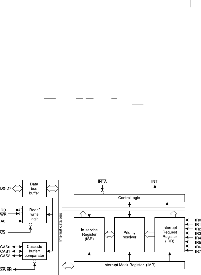
A schematic representation of Intel 8259 priority interrupt controller (PIC) is presented in Figure 8.10 .
Interfacing signals shown in the diagram may be sub-divided in three separate groups. Signals within
the top-half, i.e., INT, INTA, D0 – D7, RD, WR, A0 and CS are for interfacing with the processor. INT
may be connected with any interrupt input pin of the processor and INTA is the interrupt acknowledge-
ment signal generated by the processor after receiving an interrupt from INT.
Signals accommodated at the right side of the diagram, i.e., IR0 – IR7 are to be used for receiving
interrupt signals from various external interrupting devices. Therefore, if the maximum number of
interrupting devices from external world is eight, then only one 8259 is suf cient for the processor,
demanding only one interrupt line of the processor. In such a situation, remaining signals, namely
CAS0, CAS1, CAS2 and SP/EN have no usage. Then, why are they provided? Well, if the number of
external interrupting devices is more than eight, then only one 8259 would not be suf cient and few
more must be added to cater to the demand. Remember, we need to use only one interrupt input pin of
the processor. If we have to use multiple 8259, then they must be cascaded (in the fashion of fan-out)
Figure 8.10 Schematic of priority interrupt controller 8259
M08_GHOS1557_01_SE_C08.indd 249M08_GHOS1557_01_SE_C08.indd 249 4/29/11 5:15 PM4/29/11 5:15 PM

250 Computer Architecture and Organization
and in that situation these remaining signals (CAS0 and so on) would be necessary for the purpose of
interfacing. Does it sound very complicated? As a matter of fact, we have encountered only half of the
story. Note that the hardware interfacing must be followed by software initialization to make any 8259
a working unit. And to avoid complexity, we shall take up only one 8259 initially, assuming the maxi-
mum number of external interrupting devices would not exceeding eight. Once we have gone through
its initialization details and working mechanism, the more complex situation involving multiple 8259
would be discussed.
8.7.1 8259 Without Cascading
If the number of interrupting devices is eight or less, then interrupt generating signal from each device
may be connected with IR0 through IR7 inputs of the interrupt controller, 8259. From the processor
side, the necessary interfacing would be INT connected with the interrupt input of the processor and
INTA from its interrupt acknowledgement output. Remaining address, data and control signals interfac-
ing also must be completed. As only one 8259 is used in the system, its SP/EN input should be pulled
high (connected with Vcc). Remaining three pins, CAS0, CAS1 and CAS2 may be left without any
connection (NC or no connection). All these complete the essential hardware interfacing.
Now comes the software part. To make 8259 completely operational, some initialization through
software commands are essential. Note that unlike 8255, 8259 does not have any reset input to initialize
some default functions. The most critical matter for this initialization procedure is to convey to 8259 to
generate and communicate separate branching address for each interrupt input to 8259. These branching
addresses are extracted by the processor from 8259 with the help of INTA signal. Whenever the INTA
goes low, 8259 sends the related branching address to the processor. But how does 8259 generate differ-
ent branching addresses for each individual interrupt attached with it through IR0 – IR7? The answer is,
a base address and its offset bytes are communicated by the processor to 8259, during the initialization
process. For this purpose, a total of four ICW (Initialization Command Word) may be sent to 8259 in
sequence, by the processor. These are designated as ICW1, ICW2, ICW3 and ICW4. If only one 6259 is
in the circuit, as in the present case, then ICW3 is not necessary and ICW4 may be communicated right
after ICW2. A15 to A8 of the base address of interrupt vector are passed to 8259 through ICW2. A7 to
A5 of the base address are communicated through ICW1. Note that A4 to A0 of the base address are
always represented by 0s. The reader may go through the data sheets of 8259 for further initialization
details of 8259.
8.7.2 8259 with Cascading
When the number of interrupting devices is more than eight, multiple 8259s must be used in cascade
con guration, as indicated in the schematic of Figure 8.11 . We may observe from this diagram that a
maximum of 64 external devices may be interfaced with eight numbers of 8259, which we designate as
follower 8259s. The INT output of these eight follower 8259s are to be interfaced with a leader 8259.
Finally, the INT output of the leader 8259 is interfaced with the interrupt input pin of the processor
(INTR). Note that all other addresses, data and control signals from the processor must be properly
interfaced with the leader as well as all eight follower 8259s. Each 8259 must be separately initialized
by the processor, as indicated in Section 8.6. In this case, ICW3 would be necessary to be sent, which
was not so in our single 8259 case.
M08_GHOS1557_01_SE_C08.indd 250M08_GHOS1557_01_SE_C08.indd 250 4/29/11 5:15 PM4/29/11 5:15 PM
..................Content has been hidden....................
You can't read the all page of ebook, please click here login for view all page.