

254 Computer Architecture and Organization
serviced by the processor of the computer. Subroutines related with these operations of reset initializa-
tion and interrupt service are stored in a suitable place, generally within the hard disc, as per the direc-
tion and knowledge of the operating system. The operating system labels these subroutines as the device
driver for the mouse and evokes the necessary one as per the system demand.
Therefore, we may readily conclude that every device must have its own device driver. Moreover, the
same device with a different manufacturer or version should be having a different driver. For example,
the device driver for a Microsoft mouse may not be suitable for a Logitech mouse. That is the reason for
supplying the related driver with any peripheral device, which must be properly stored by the operating
system at the time of its installation.
8.10 STANDARD I/O INTERFACES (BUSES)
From the discussions so far, the reader must have understood that the input/output system for a com-
puter are accommodated in many layers, like memory devices. We have already discussed about cache
memory and a special high speed bus to communicate with it, designated as cache bus ( Figure 8.13 ).
Main memory of the system is also interfaced with the processor with a dedicated memory bus so that
delay in I/O operations, which is quite normal and happens frequently, does not retard the instruction
that has to be carried out.
The innermost layer of I/O devices is directly interfaced with the processor through its address,
data and control bus (designated as I/O bus), and communicates in synchronous manner (synchronous
parallel communication). Note that although with processor these devices communicate in synchronous
fashion, with the external world they communicate in asynchronous manner. Example of I/O devices
of this layer may be 8255-based ports, timers/counters for real-time operations, USART for serial com-
munication and other similar devices. Note that 8255 communicates with its processor in synchronous
manner while it functions asynchronously with the external world.
The outermost layer of devices is never directly interfaced with the processor through the processor
bus as many of those have their own processors. Examples of these devices are printer, display, key-
board, mouse and so on. The interfacing technique of these devices with the host (computer) is generally
Figure 8.13 Schematic of layered bus structure adopted in computers
M08_GHOS1557_01_SE_C08.indd 254M08_GHOS1557_01_SE_C08.indd 254 4/29/11 5:15 PM4/29/11 5:15 PM
Input / Output Organization 255
prescribed by the manufacturer. It may be serial or parallel, but never synchronous. The outermost bus
for I/O communication is interfaced with the innermost processor-bus through some bridge ICs. For
example, the PCI bus originates from the PCI bridge and SCSI bus originates from SCSI controller,
which is another bridge IC (Figure 8.13 )
8.10.1 Genesis of Interfacing Buses
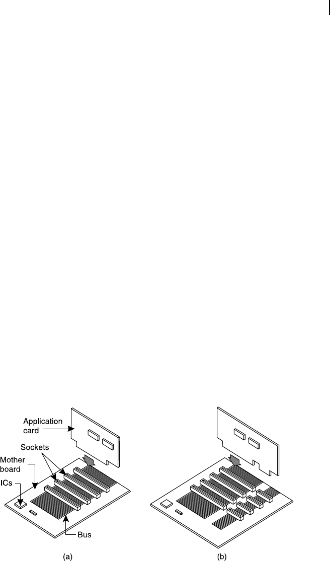
With the introduction of IBM PC, a standard evolved for the internal bus generated by the proces-
sor and some of its peripherals. This bus contained 20 address lines, 8 data lines and some control
signals in the form of memory read, memory write, I/O read and I/O write, all extracted from the
processor (8088 to be precise), along with some interrupt-related and DMA-related signals summing
up to a total count of 62 signal lines. On the motherboard, this bus was extended up to one edge
and a few sockets were connected in parallel, so that add-in application cards, with 31 connecting
plates on either side of its PCB, might be plugged directly into these sockets as and when necessary
[ Figure 8.14 (a)].
However, with the introduction of Intel 80286 processor, the con guration of this PC bus has
changed. The number of data lines became 16 and the number of address lines also increased. If a
completely new bus was introduced, existing cards and their manufacturers would have been obso-
lete; which cannot be taken as a happy solution. This problem was resolved by maintaining the previ-
ous con guration unchanged and incorporating all new signals as a separate bunch and introducing
one new connector with 36 contacts, placed at the side of each existing connector [Figure 8.14 (b)].
Incidentally, at a later stage, this bus (with some minor variations) was designated as industry stan-
dard architecture ( ISA ) bus and adopted by most of the manufacturers. Later it was modi ed to
extended industry standard architecture ( EISA ) bus to deal with 32-bit architecture, an improvement
at that time. Peripheral component interconnect ( PCI ) is another bus, introduced by Intel in 1992,
which is widely adopted till today for its capability of processor independency, high speed data trans-
fer and relatively lower cost.
With further development of computer industry, more variation and, therefore, more standard-
ization came into play for these I/O interfacing techniques. These are referred as standard bus or
Figure 8.14 (a) First IBM PC bus (b) PC/AT bus
M08_GHOS1557_01_SE_C08.indd 255M08_GHOS1557_01_SE_C08.indd 255 4/29/11 5:15 PM4/29/11 5:15 PM

256 Computer Architecture and Organization
interfaces and offers documented references for their characteristics. Three of such widely adopted
buses are
R USB or Universal Serial Bus
R SCSI of Small Computer System Interface
R GPIB/HPIB/IEEE488
We shall now discuss about these three buses for their functionality and basic characteristics.
However, we should keep in mind that these are not the only three buses available in the computer
industry. There are quite a few more buses, which are adopted as and when the necessity was felt.
VME bus, Multibus , I
2
C bus, JTAG and so on are to name a few of such buses, each one offer-
ing some unique advantage of their own. Finally, we must remember that these new buses are not
processor bus (do not originate directly from the processor) but a modi ed form, which is able to
communicate with the processor bus at one end and different types of external peripheral devices at
the other end.
8.10.2 Universal Serial Bus (USB)
In early days of computers, attaching any new peripheral device with the host, demanded cer-
tain procedures. Most of these devices were shipped with their own interfacing cards to be plugged
in one of the available bus connectors (Figure. 8.14). For this purpose, the system must be switched off,
the computer’s chassis has to be opened and the interfacing card needs to be plugged in. Some of these
cards demanded additional settings of built-in micro-switches or jumper connections. In case of any
con ict with the assigned address by the user with addresses of other already existing cards, it must be
resolved by the user at the same time. Finally, the chassis needs to be reassembled as it was, the com-
puter to be switched on, the device has to be con gured and then the system must be rebooted.
To eliminate this problem, in the year 1993, several reputed manufacturers (including Intel, Micro-
soft, IBM) came together to set up a new standard interface for low-speed devices, so that it may be
plugged-in or removed without the need of opening the chassis or rebooting the computer. To maintain
the number of pins to a minimum, the serial interface was selected, rather a parallel interface. Further-
more, it was decided that the power necessary for the device must be supplied through the interface
itself, thus eliminating the need of a separate or additional power supply for the device to be interfaced.
The outcome of all these planning was the USB or universal serial bus version 1.0 and then 1.1. At a
later date, version 2.0 was also released and presently used in most of the systems. USB 2.0 operates
at higher speed and is backward compatible with USB 1.1 and USB 1.0. Figure 8.15 (a) depicts the
USB logo, which is very well-planned and explains the basic characteristics of USB, as indicated in
Figure 8.15 (b).
This might be the reason of mushrooming of computer-quacks at that era of computers. What
a procedure!!
F
O
O
D
F
O
R
T
H
O
U
G
H
T
M08_GHOS1557_01_SE_C08.indd 256M08_GHOS1557_01_SE_C08.indd 256 4/29/11 5:15 PM4/29/11 5:15 PM
Input / Output Organization 257
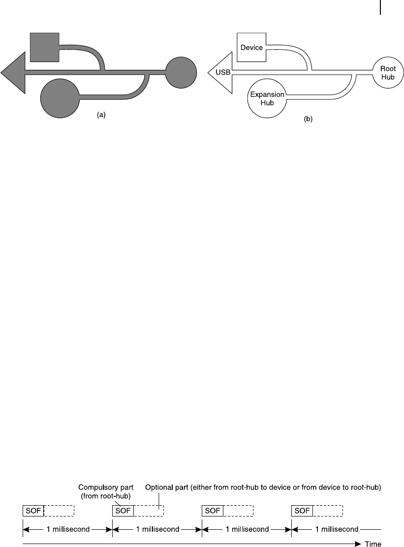
Figure 8.15 (a) Logo and (b) structure of USB
USB is essentially a four-pin interface, one pin each to carry power (+5V), ground, and the remaining
two for data signals. The interface originates at the processor level through a root-hub and branches like
a tree, thereafter. A maximum of 127 devices may be interfaced with the root through the primary or
secondary hubs [the logo of USB in Figure 8.15(b)]. Logic 0 is represented by an oscillation of voltage
transition (low to high or high to low), while logic 1 is represented by an absence of voltage transition.
Therefore, a continuous 0 would generate a square wave like pulses and continuous 1 would maintain a
steady state of voltage (either at low or at high, depending upon the initial state). The rate of data trans-
fer (bandwidth) for USB version 2.0 is 480 Mbps as compared to 12 Mbps of version 1.1 and 1.5 Mbps
of version 1.0. The higher bandwidth is suitable for multimedia, while lower values may serve well for
printer, keyboard and similar slower devices.
Although the communication technique adopted in USB is a serial one, there is a difference with
the classical serial communication concept, which we have already discussed in Section 8.4. At every
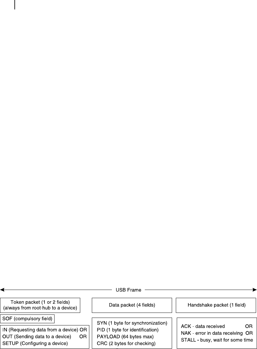
millisecond, irrespective of whether any device is interfaced with the USB root-hub or not, the root-hub
initiates (broadcasts) a frame to maintain the synchronization for all devices. This initiation is indicated
by a packet , designated as SOF or start of frame. Note that any frame is composed of several packets
(SOF is also a packet) as per the requirement of data transfer ( Figure 8.16 ). Therefore, when initiated
by the root-hub by the packet SOF, the remaining part of the frame may contain some data from either
the root-hub or from any device or might not contain any data packet at all. This third case is known as
idle frame. We must remember here that in USB, the communication is always from root-hub to device
or from device to root-hub but never from any device to another device .
Depending upon the possible type of contents, USB frames may be classi ed as follows:
R Control
R Bulk
R Isochronous
R Interrupt
Figure 8.16 Initialization of frames from USB root-hub at every millisecond
M08_GHOS1557_01_SE_C08.indd 257M08_GHOS1557_01_SE_C08.indd 257 4/29/11 5:15 PM4/29/11 5:15 PM
258 Computer Architecture and Organization
In the case of a new device to be con gured or its status to be investigated or some commands to be
issued to a device, control frames are used. When a large volume of data need to be communicated to or
from the root-hub without any real-time restraint (e.g., in the case of printers), the bulk frames are used.
Isochronous frames are meant for real-time data transfers (for example, animation or music). As the
USB does not support interrupts, the problem of responding to it is solved by interrupt frames, which
are initiated at regular intervals to check any pending interrupt from any device and if af rmative, then
respond accordingly.
Packets within any frame may be of four types, in USB. These four types are
R Token packets
R Data packets
R Handshake packets
R Special packets
Token packets are for controlling various devices attached with the root-hub and their ow-direction is
always from the root-hub to the devices attached. Token packets contain information like SOF, IN, OUT
and SETUP. Note that SOF is always the leading packet in any frame. OUT packet, which (if present)
immediately follows the SOF packet, indicating that the data packet of the frame is for a device, being
sent by the root-hub. The address of the target device, which needs to receive the data, is encrypted
within this OUT packet. IN packets are used to ask data from devices, one at a time, which may be
considered as a sort of polling. SETUP packets are used for con guring a particular device interfaced
with the root-hub of USB.
The data packet of USB contains four elds, SYN, PID, PAY LOAD and CRC and this packet may
be transmitted in either direction, i.e., either to the root-hub or from the root-hub. The synchroniza-
tion eld SYN has a width of 8-bit and always leads the data packet. This is followed by the packet
identity eld PID having a width of another 8-bit. Next eld is the PAY LOAD or data proper, which
is restrained to a maximum width of 64 bytes. The last eld of all data packets is a 16-bit eld, CRC,
which indicates cyclic redundancy check for error detection. If any error is detected through this eld,
then the same data packet must be sent again, except for isochronous frames.
The handshake packet may contain any one of the following three information ACK (for no CRC
related error), NAK (because of CRC related error) and STALL (to wait). A summary of above discus-
sions is presented in graphical form in Figure 8.17 .
Figure 8.17 Classification and types of packets in USB communication
M08_GHOS1557_01_SE_C08.indd 258M08_GHOS1557_01_SE_C08.indd 258 4/29/11 5:15 PM4/29/11 5:15 PM
..................Content has been hidden....................
You can't read the all page of ebook, please click here login for view all page.