
Microprogramming and Microarchitecture 281
9.6 SEQUENCING AND EXECUTION
OF MICROINSTRUCTIONS
In Section 9.5, we have discussed about microinstructions, in general. However, we have not discussed
in details about their sequencing or execution as we intend to discuss those in this section. For the pur-
pose of clarity, we discuss various aspects of these issues with three examples, which we have partially
solved throughout this chapter. Our rst example is related with the instruction Load accumulator by
R0 . The next example would be Store accumulator in R0 . The third example would be related with the
instruction Add accumulator with R0 .
9.6.1 Example 1 (Load Accumulator by R0)
All microinstructions with their sequence for execution of the instruction Load accumulator by R0 are
presented within rst three rows of Table 9.6 . Last three rows of this table accommodate microinstructions
for Save accumulator in R0 , which we shall discuss later. Although there are 18 control signals accommo-
dated within 18 columns of Table 9.6 , the reader need not be worried about the complexity of the ongoing
discussions, as we are concerned about only four control signals, considering both instructions and they
are reduced to only two if we consider the instruction of our rst example, i.e., Load accumulator by R0.
These two control signals are ENA0 and S5. As it may be observed in Table 9.6 , columns representing
only these two control signals are not shaded for rst three rows. We may neglect the shaded columns at
present as they output logic high (1) in all sequences and remain passive (does not take part in execution
of the ongoing instruction).
Sequence C0 C1 C2 C3
EN
A0
EN
A1
EN
A2
EN
A3
EN
X0
EN
X1
EN
X2
EN
X3 S1 S2 S3 S4 S5 S6
T1 111101111111111111
T2 111101111111111101
T3 111111111111111111
T1 111111111111111110
T2 011111111111111110
T3 111111111111111111
Table 9.6 Microinstruction sequencing for instructions: (1) Load accumulator by R0
and (2) Save accumulator in R0
Before proceeding further with our example, let us take a look at Figure 9.6 , where we have presented
the timing diagram of the instruction Load accumulator by R0 , the instruction that is under discussion at
present. If we observe this timing diagram, we nd that rst ENA0 changes from high to low, enabling
register R0 to allow its data to accumulator through the bidirectional bus [Figure 9.3 (b)]. After that, S5
changes from high to low and its falling edge is used to latch the data presently available in accumulator.
As per the timing diagram, S5 then changes from low to high, necessary for another latching if required in
future. Finally, ENA0 changes from low to high disabling the output of R0 to the bidirectional data bus.
Now, this last change (ENA0 from low to high) may be initiated at the same time of changing S5 from
low to high without sacri cing anything for the data transfer from R0 to accumulator. On the other hand, it
would reduce one state of required timing for the execution of the instruction. Therefore, our sequence of
M09_GHOS1557_01_SE_C09.indd 281M09_GHOS1557_01_SE_C09.indd 281 4/29/11 5:17 PM4/29/11 5:17 PM
282 Computer Architecture and Organization
loading data from R0 to accumulator would contain only three states, T1, T2 and T3, as indicated in Table
9.6 ( rst three rows). The rst row in this table shows that at T1, only ENA0 has to be changed to low (0),
enabling R0 for accumulator and all other signal would remain high. Next, in T2, S5 must be 0, which
executes latching of the data from R0 within the accumulator. Note that ENA0 remains unchanged (at 0)
at this stage. Finally, at T3, all signals, including ENA0 and S5 are high (1), completing the data transfer
process. The reader may now compare Table 9.2 with Table 9.6 and would nd that four steps in Table 9.2
had been reduced to three steps in Table 9.6 , without sacri cing the performance of the processor.
9.6.2 Example 2 (Save Accumulator in R0)
For our second example, we have selected the instruction to save accumulator in R0. Sequencing of all
control signals is shown in last three rows of Table 9.6 . In this case (Figure 9.3 ), S6 is pulled down (0)
at T1, enabling accumulator’s data available in the bidirectional data bus, connected to all four registers
(R0 – R3). The data are latched within R0 at T2 by changing C0 from high to low. Finally, at T3, all
signals including C0 and S6 are brought back to high level. Table 9.3 may be compared with Table 9.6
and the reader would readily observe that we have reduced the necessary steps from four to three.
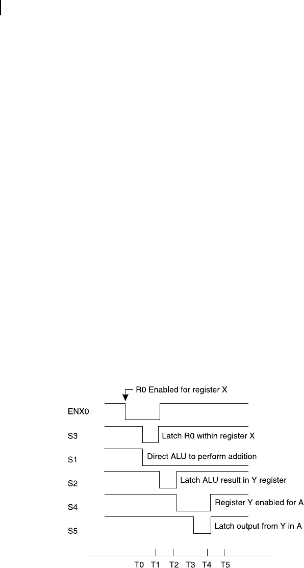
9.6.3 Example 3 (Add Accumulator with R0)
In Table 9.4 , we have already presented the steps of activating different control signals for adding the
content of register R0 with accumulator. Note that there were 10 steps in total. This may be reduced to six
steps from T0 to T5, if we coordinate the sequencing of different control signals correctly. The modi ed
timing diagram for implementing this addition instruction is shown in Figure 9.8 . In Table 9.7 , we have
presented all control signals (e.g., Table 9.6 ) indicating the sequence of necessary changes in relevant
signals. Therefore, Figure 9.8 and Table 9.7 present the same information, but in different formats. In
Table 9.7 , the highlighted column entries represent those signals, which are passive for implementing our
example instruction, add accumulator with R0 . All these control signals remain high for all sequences and
presented just for the purpose of complete visualization.
Figure 9.8 Timing diagram of execution of Add R0 with a instruction
M09_GHOS1557_01_SE_C09.indd 282M09_GHOS1557_01_SE_C09.indd 282 4/29/11 5:17 PM4/29/11 5:17 PM
..................Content has been hidden....................
You can't read the all page of ebook, please click here login for view all page.