

Microprogramming and Microarchitecture 283
Let us now investigate the sequences necessary to add R0 with accumulator. To start with, R0 must
be copied to X register. This is to be done in two steps. At T0, ENX0 is made low (0) to allow data in
R0 to be available in register X through the unidirectional bus. This is latched within register X by high
to low transition of S3 (refer Figure 9.3 ), implemented in sequence T1 of Table 9.7 . Note that at the
same sequence T1, ENX0 is maintained as 0 and S1 is also changed to 0, enabling the ALU to perform
the addition. It may be noted that we have not changed S1 throughout the sequences as in case of any
eventual subtraction it would be changed to 1. Had there been more ALU functions provided for, then it
would have been customary to bring back S1 to its original state of logic 1 (high).
In the third sequence, i.e., T2, both ENX0 and S3 are brought back to high state as the latching
operation for register X is complete. As our ALU is a static one (output is available instantly), at the
same instant of T2, ALU output is latched within Y register by the control signal S2 (Figure 9.3 ). Now
the addition operation is over and the remaining duty is to transfer the result of addition at register Y to
accumulator. For this purpose, sequence T3 is used to enable register Y by making the control signal S4
low so that its output may reach the accumulator. At the same time S2 is also brought back to its high
state as the latching operation of ALU output in Y register is over.
Sequence
C
0
C
1
C
2
C
3
EN
A0
EN
A1
EN
A2
EN
A3
EN
X0
EN
X1
EN
X2
EN
X3
S
1
S
2
S
3
S
4
S
5
S
6
T0 11111111 0 111111111
T1 11111111 0 111010111
T2 11111111 1 111001111
T3 11111111 1 111011011
T4 11111111 1 111011001
T5 11111111 1 111011111
Table 9.7 Microinstruction sequencing for instruction: Add accumulator with R0
T4 is the next sequence, when S5 becomes low, latching the data from Y register within the accumu-
lator. Note that S4 remains low during this sequence so that the data is available within the accumulator
from Y. Once the latching of ALU result within accumulator is over, the last sequence T5 is used to bring
back S4 and S5 to their original high state.
9.7 SOLVED EXAMPLE
For the purpose of understanding the complexity of designing a hardwired control unit for generating
microinstructions, we now take up a simpler problem, say a smaller part of our previous problem. We
de ne the problem in details and then solve it step by step so that all necessary details are explained
properly.
Problem
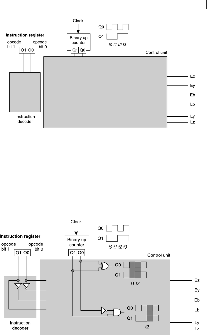
Three registers B, Y and Z are interconnected by a bidirectional data path as shown in Figure 9.9 (a).
Considering only four instructions as indicated in Figure 9.9 (c), necessary control signal descriptions
are presented in Figure 9.9 (b). Figure 9.9 (d) shows the timing diagram of the necessary control sig-
nals to implement each instruction. Assuming that the system clock is available, design the instruction
decoder and then a hardwired control unit to implement these functions.
M09_GHOS1557_01_SE_C09.indd 283M09_GHOS1557_01_SE_C09.indd 283 4/29/11 5:17 PM4/29/11 5:17 PM

284 Computer Architecture and Organization
Solution
To solve this problem and to design the control unit, we assume that the opcode is only two-bit wide, as
shown in Figure 9.9 (c). The basic structure of the unit would be similar to that as shown in Figure 9.5 .
The system clock signal would be one of the two inputs of the control unit, which would govern the sequence
of activities of relevant control signals. These control signals are to be generated as per the requirement of
opcodes, which would be the other input for the control signal generation. For this purpose some instruction
decoder would be necessary. The basic scheme of the overall system is presented in Figure 9.10 .
Note that in Figure 9.10 , two void rectangles (lightly shaded) are shown. The larger of the two rect-
angles represent the control unit, whose hardware details we are going to design step-by-step. The other
one, the smaller rectangle represents the instruction decoder. Also note that all desired output signals
from the control unit are marked properly. Input for the instruction decoder would be derived from the
ongoing opcode, assumed to be loaded and available within the IR. Output from a 2-bit binary up-counter
driven by the system clock would be one of the inputs of the control unit.
Step 1 Instruction decoder
Our rst step should be to take up the design of the instruction decoder. From Figure 9.9 , we nd that
LSB (O0) of the 2-bit opcode indicates the concerned register, either Y or X for all instructions. If this
LSB is 0 then register Y is indicated. If this bit is 1, then register Z is indicated. On the other hand, the
MSB of the 2-bit opcode (O1) indicates the type of instruction, either loading or saving register B. If this
is a case of loading register B, then this MSB of opcode is 0. On the other hand, for a case of saving B,
this bit becomes 1. Note that there is no other direct correlation between these opcode bits. Therefore,
each of these two bits of the opcode (available within instruction register) may be individually decoded
as either inverted or non-inverted, as shown in Figure 9.11 . This scheme of decoding generates four
output signals from the instruction decoder block, which are fed to the control unit.
Step 2 Timings
To design the control unit, we start with the timing sequences. From Figure 9.9 (d), we may observe that
all control signals (a total of six) are active during either t1 or t2 time-slots. During other time-slots, i.e.,
t0 and t3 , all of them remain high and inactive. Moreover, the enabling signals, namely Ey, Ez and Eb,
are active in both t1 and t2 time-slots, while the latching signals, namely Lb, Ly and Lz are active during
t2 time-slot only. Therefore, from the four time-slots ( t0 , t1 , t2 and t3 ) generated by the 2-bit up-counter,
we need to generate some signals, which would indicate these time-slots properly. Note that these two
time-slices are darkly shaded in the counter-output timing diagrams in Figure 9.11 .
Figure 9.9 Registers, data path, instruction details and control signals for example
problem
M09_GHOS1557_01_SE_C09.indd 284M09_GHOS1557_01_SE_C09.indd 284 4/29/11 5:17 PM4/29/11 5:17 PM
Microprogramming and Microarchitecture 285
To generate an active signal to indicate both t1 and t2 time-slices, we observe that the counter outputs
Q0 and Q1 are complementary to each other. In other words, if Q0 is low then Q1 is high. If Q0 is high
then Q1 is low. Therefore, we may use the 2-input XOR gate with inputs as Q0 and Q1. The output of this
XOR gate would be high during t1 and t2 . However, during t0 or t3 , output from this XOR gate would
be low. This part of the circuit is shown at the top portion of the larger shaded rectangle of Figure 9.11 .
To generate a signal exclusively to indicate t2 , we nd that Q0 is low and Q1 is high during this time-
slice. Therefore, we invert Q0 and the output of the inverter is logically ANDed with Q1 to generate
the indication signal, which would be 1 only during t2 and during t0 , t1 and t3 it would go low (0). The
reader is encouraged to make a truth table and verify this statement. This part of the circuit with one
inverter and one AND gate is shown at the bottom part of the larger shaded rectangle of Figure 9.11 .
Figure 9.10 Basic I/O scheme of instruction decoder and control unit
Figure 9.11 Design details of instruction decoder and relevant clock states
M09_GHOS1557_01_SE_C09.indd 285M09_GHOS1557_01_SE_C09.indd 285 4/29/11 5:17 PM4/29/11 5:17 PM
286 Computer Architecture and Organization
Therefore, for the next part of design, whenever we need to generate a control signal, which would
remain active during t1 and t2 (only three enabling signals in our example case), then we may use the
output of the XOR gate to trigger the signal. On the other hand, when we need to generate a control
signal meant to be active only during t2 (three latching signals in our example case), we should activate
it using the output of the AND gate.
Step 3 Enabling signals
In the next step of our design process, we take up all three enabling signals, Ey, Ez and Eb. Note that all
of these three control signals are active (low) only during t1 and t2 time-slices. Therefore, the output from
the XOR gate would be the major input for these three cases. From Figure 9.9 (c) and (d) we nd that Ey
should be low only if O1 (MSB of opcode) is low and O0 (LSB of opcode) is low. As Ey has to be active
low, we incorporate a three-input NAND gate to generate Ey. Inverted output from O0 and inverted out-
put of O1 along with the output from the XOR gate would be three inputs for this NAND gate.
To generate Ez signal, we need to use another three-input NAND gate. In this case, the inputs would
be the output from XOR gate (so that it is active only during t1 and t2 ), inverted O1 (as Ez to be active
only when O1 is low) and direct output from O0. Refer Figure 9.12 for all these design details.
Before designing the hardware circuit to generate the control signal Eb, we should investigate the
conditions to make it active. Eb is active low and it is activated only during t1 and t2 time-slices, if
O1 (MSB of opcode) is high. The LSB of the opcode does not contribute anything about the activation
of Eb. Therefore, we place a 2-input NAND gate, with one input from the XOR gate (its output) and
another input as non-inverted O1 bit of the opcode (from instruction register). This part of the circuit is
also incorporated in Figure 9.12 and the reader is advised to spend some time to study the validity of the
circuit we have designed so far, before proceeding to the next step of the design process.
Figure 9.12 Design of enabling signals Eb, Ey and Ez
Step 4 Latching signal Lb
For the next phase of design, we take up the Lb signal, which need to be used to latch any data input in
register B [Figure 9.9 (a)]. From Figure 9.9 (d), we observe that this signal should be active only during
M09_GHOS1557_01_SE_C09.indd 286M09_GHOS1557_01_SE_C09.indd 286 4/29/11 5:17 PM4/29/11 5:17 PM

Microprogramming and Microarchitecture 287
the time-slice t2 . We have already designed this part of the circuit with an inverter and a 2-input AND
gate to trap relevant signal phases of the counter output. Therefore, this must be one of the important
inputs to generate Lb. Furthermore, as Lb is active (low) only if the MSB of opcode is 1 [Figure 9.9 (c)
and (d)]. Therefore, the non-inverted output from O1 bit of the instruction is considered as another input
to generate Lb and a 2-input NAND gate is used for this purpose. This part of the circuit is shown in
Figure 9.13 , along with the features, which we have already designed or discussed.
Figure 9.13 Design of latching signal Lb
Step 5 Latching signals Ly and Lz
To complete our design of control signals, we now take up the cases of two more signals, namely Ly and
Lz. The rst one has to be used to latch data in register Y and the other one for register Z. Just like the
previously considered signal Lb, these two signals are also active only during the time-slice t2 . Both are
active when the MSB of opcode is 1. Ly is active when LSB of opcode is 0. Lz is active when LSB of
opcode is 1. To meet all these demands, we consider the output of the 2-input AND gate which we have
already earmarked for t2 time-slice and logically AND this signal with the MSB of the opcode, using
another 2-input AND gate. Output of this second AND gate is then used along with inverted O0 signal
to generate Ly through a 2-input NAND gate ( Figure 9.14 ). Another 2-input NAND gate is used to gen-
erate Lz using non-inverted O0 signal as shown in the same diagram. Figure 9.14 shows the complete
circuit diagram for the control unit along with the instruction decoder.
Discussions
One simpli cation or assumption has been made for this design, and it should be indicated now. In
general, the clock signal of any system would be continuously running as long as it is not switched off
or inhibited (disabled or stopped). Therefore, in our designed circuit, any sequence of control signals
as directed by the loaded opcode within the instruction register would be generated again and again
because of the continuity of the clock input. If the set of signals have to be generated only once, there
must be some additional circuit to stop the counter (the 2-bit counter in our example case) after comple-
tion of t3 . For executing another instruction, the counter must be reset and started fresh.
M09_GHOS1557_01_SE_C09.indd 287M09_GHOS1557_01_SE_C09.indd 287 4/29/11 5:17 PM4/29/11 5:17 PM
..................Content has been hidden....................
You can't read the all page of ebook, please click here login for view all page.