

Microprogramming and Microarchitecture 291
is reduced to a considerable extent. In this modi ed case, we are enabling the output buffers only for
the duration of t1 and not for both t1 as well as t2 , like the previous case, as it was explained through
Figure 9.17 . The rising edge of the clock signal immediately after this enabling is inverted to generate
a falling edge to latch the data.
9.9 PROCESSOR DATA PATH DESIGN
Every processor would have multiple internal locations to hold temporary data and there is a need to allow
the data to ow from one point (location) to another. We are already familiar with a few of these locations,
like general purpose registers, accumulator, result register, program counter, stack pointer and so on. To
allow a proper data ow incorporating these location, every processor provides the necessary data path(s).
The detailed design of data path depends on various factors, which are beyond the scope of the present
work. Moreover, every processor has its own design concepts and there is no single standardized technique
in this aspect. However, some basic guidelines for this data path design need to be discussed at this stage.
For the purpose of this discussion, we shall consider the following registers of the processor:
R Eight general purpose registers (R0 – R7)
R Accumulator (A)
R Stack pointer (SP)
R Program counter (PC)
R Memory address register (MAR)
R Memory buffer register (MBR)
R Result register of ALU (Z)
Figure 9.18 Modified circuit diagram of the control unit
M09_GHOS1557_01_SE_C09.indd 291M09_GHOS1557_01_SE_C09.indd 291 4/29/11 5:17 PM4/29/11 5:17 PM
292 Computer Architecture and Organization
R Temporary register for ALU operand input (Y)
R Instruction register (IR)
The reader may note that most of the operations (excluding interrupt servicing or DMA etc.) of any
processor are oriented around these registers along with its ALU. It was already indicated that major
processor operations are:
R Fetch instruction (use PC, MAR and MBR)
R Decode instruction (use MBR and IR)
R Fetch operand (use MAR, MBR, general purpose registers)
R ALU operation (use ALU, related registers for operand, result register Z)
R Store result (use Z, general purpose registers or MBR and MAR for external storage)
R Call and return (use SP, MAR, MBR, PC)
R Increment PC (use PC, ALU, Z)
R Increment/decrement SP (use SP, ALU, Z)
Here, we have identi ed speci c registers along with these standard operations. We may now conclude
that major data ow for a smooth operation of the processor would need communication channels
between these registers along with the ALU.
Thus, we see that the data path is always associated with ALU, because all major operations of the pro-
cessor are concerned with its ALU. In general, the ALU needs two operands as input and generates the result
of its operation as output. Therefore, we may assume that these three data sets must properly ow to and
from ALU by the designed data path. Note that the operands may be within any register and the result also
might have to be shifted (copied) to any register. Therefore, all of these registers have to be interfaced prop-
erly through the data path as per the data ow requirements. The width of this data path must cater to the
width of these registers. At present, for the purpose of simplicity, we assume that the registers are of 8-bit.
Depending upon the design requirements, the number of data paths may be one, two or three. An
example with only one data path is shown in Figure 9.19 . The data path is designated as C-Bus . Although
there is no such rule, however, the general practice is to designate the data path, which carries the result
of the ALU operation as the C-Bus. A-Bus and B-Bus are generally related with the operands of the
ALU, which we shall discuss a little later. At present, we may note that A-Bus and B-Bus are expected to
communicate data between the registers indicated above and the ALU input register(s) to send operands
from registers to ALU. Note that C-Bus is a must for any processor as it is associated with the result of
ALU. When there are two data paths, one is C-Bus and the other is designated as B-Bus. The general
practice is not to designate them as C-Bus and A-Bus.
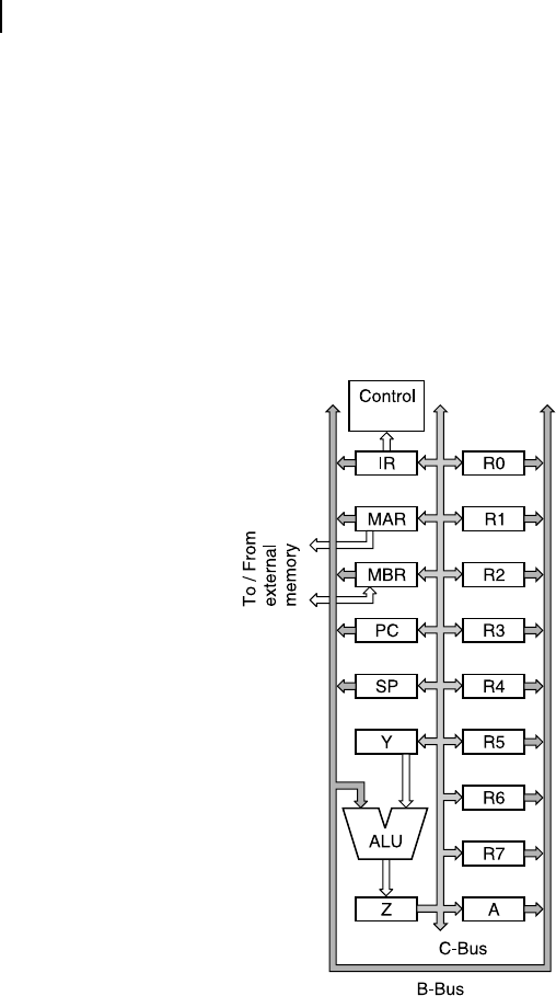
9.9.1 One Data Path (C-Bus)
When the processor has only one data path, the C-Bus, as shown in Figure 9.19 , the design becomes
economical although the speed of processor operation is somewhat restricted. It is needless to elaborate
the fact that more number of data path would lead to more wafer space resulting in more expenses.
However, the sequence of data ow is evidently restricted by only one data path as we shall investi-
gate it now, using a simple example case and referring Figure 9.19 . We must remember that C-Bus is a
bidirectional data bus and only for register Z it is unidirectional. Data are allowed to move out from Z
register but cannot be placed within Z register through the C-Bus.
M09_GHOS1557_01_SE_C09.indd 292M09_GHOS1557_01_SE_C09.indd 292 4/29/11 5:17 PM4/29/11 5:17 PM

Microprogramming and Microarchitecture 293
Let us assume that the processor has to execute an addition instruction and its two operands are
presently available in two registers, say R4 and R5. We also assume that the result of this operation
has to be stored within the accumulator, i.e., register A. Using the data path or C-Bus of Figure
9.19 , the control unit would rst copy the data in R4 within ALU input register Y. After that the
control unit would allow the data within register R5 available within the C-Bus and allow the ALU
to perform the addition. Note that the result of addition would be immediately available within
the ALU output register Z through the local bus connecting it with ALU output. Now the control
unit would activate necessary control signals to copy the data from Z to A. We may summarize the
involved steps as follows:
R Step 1 : Copy R4 into Y
R Step 2a : Allow R5 to C-Bus
R Step 2b : Perform addition through ALU, result in Z
R Step 3 : Copy Z into A
Steps 2a and 2b may be completed within one clock cycle, as we have discussed before. In that case,
the adding operation would require three clock cycles as per our scheme. Therefore, we may conclude
that the processor would be able to complete its operation with only one bus spending three clock
cycles. Now let us consider an improved situation with two data paths, C-Bus and B-Bus, as shown in
Figure 9.20 .
Figure 9.19 Design with single data path
M09_GHOS1557_01_SE_C09.indd 293M09_GHOS1557_01_SE_C09.indd 293 4/29/11 5:17 PM4/29/11 5:17 PM
294 Computer Architecture and Organization
9.9.2 Two Data Paths (B-Bus and C-Bus)
When we allow two separate data paths interfaced with ALU, as shown in Figure 9.20 , the B-bus may
be used to transport the operand from R5 at the same time of transporting R4 to Y register. The steps
required to complete the same addition operation would now be modi ed as:
R Step 1 : Copy R4 to Y through C-Bus and R5 to ALU by B-Bus and perform addition operation
through ALU. The result would be in Z register.
R Step 2 : Copy Z into A using C-bus.
Therefore, now we can conclude that instead of three cycles, with the present con guration the proces-
sor would need two clock cycle to complete the same addition operation.
Is it possible to improve the performance further by incorporating another data path in the sys-
tem architecture? To evaluate that, we incorporate another bus, A-Bus, as shown in Figure 9.21 .
As both A-Bus and B-Bus are capable of simultaneously sending two operands from R4 and R5,
the C-Bus now remains completely free to transport the result of the operation from Z to A. As all
these may be completed in one clock cycle, the whole addition operation may be completed by
one cycle.
unit
Figure 9.20 Design with two data paths
M09_GHOS1557_01_SE_C09.indd 294M09_GHOS1557_01_SE_C09.indd 294 4/29/11 5:17 PM4/29/11 5:17 PM
..................Content has been hidden....................
You can't read the all page of ebook, please click here login for view all page.