

Control Unit Operation 303
R React against interrupts.
R React against any DMA request.
R React against any power management command.
It is needless to mention that any one of above-mentioned groups may be divided to several sub-
groups. For example, the rst group may be sub-divided as instructions with or without external
operands. Similarly, interaction with external memory may be sub-divided into reading and writing
and so on. However, nally all operations of the processor must be transformed to a set of micro-
operations. So, let us spend some time to study these micro-operations.
10.3 MICRO-OPERATIONS
What is meant by micro-operations? Well, it may be described as the minimum unit operation per-
formed by the processor within the smallest allowable time-slice. We have already indicated about these
time-slices in Chapter 9. There, we have shown how the system clock may be used to generate different
time-slices. Some of the examples of micro-operations occupying these time-slices are
R Enable a register to output its data through the concerned bus.
R Latch a data set available within a register.
R Direct ALU to perform increment by one operation with available operands.
As we have observed in Chapter 9, each micro-operation is performed by activating one or more
control signals. We have also demonstrated in that chapter that how the necessary control signals may
be generated as per their desired sequence either by hardware or by software. However, discussions
pertaining to fetch cycle had been left pending in that chapter as we prefer to discuss it here.
10.3.1 Fetch Cycle
By now we know that during a fetch cycle, the processor would bring a byte or word of instruction from
memory, which is located outside the processor. To implement it, the processor is assisted by several
registers. They are
R Program counter or PC
R Memory address register or MAR
R Memory buffer register or MBR
R Instruction register or IR .
The rst one, the program counter is already known to us, introduced and described in Chapter 5.
This register always holds the address of the next instruction to be fetched by the processor. In Chapter 9,
Strictly speaking, not in all cases the processor has to fetch the next instruction from external
main memory. In many cycles, the instruction word might be available within internal cache
memory, which we have discussed in Chapter 7. However, outside or inside, whatever is the
case, a fetch cycle is unavoidable for any processor.
F
O
O
D
F
O
R
T
H
O
U
G
H
T
M10_GHOS1557_01_SE_C10.indd 303M10_GHOS1557_01_SE_C10.indd 303 4/29/11 5:19 PM4/29/11 5:19 PM
304 Computer Architecture and Organization
we have come across the last one, the instruction register (IR), which holds the ongoing instruction and
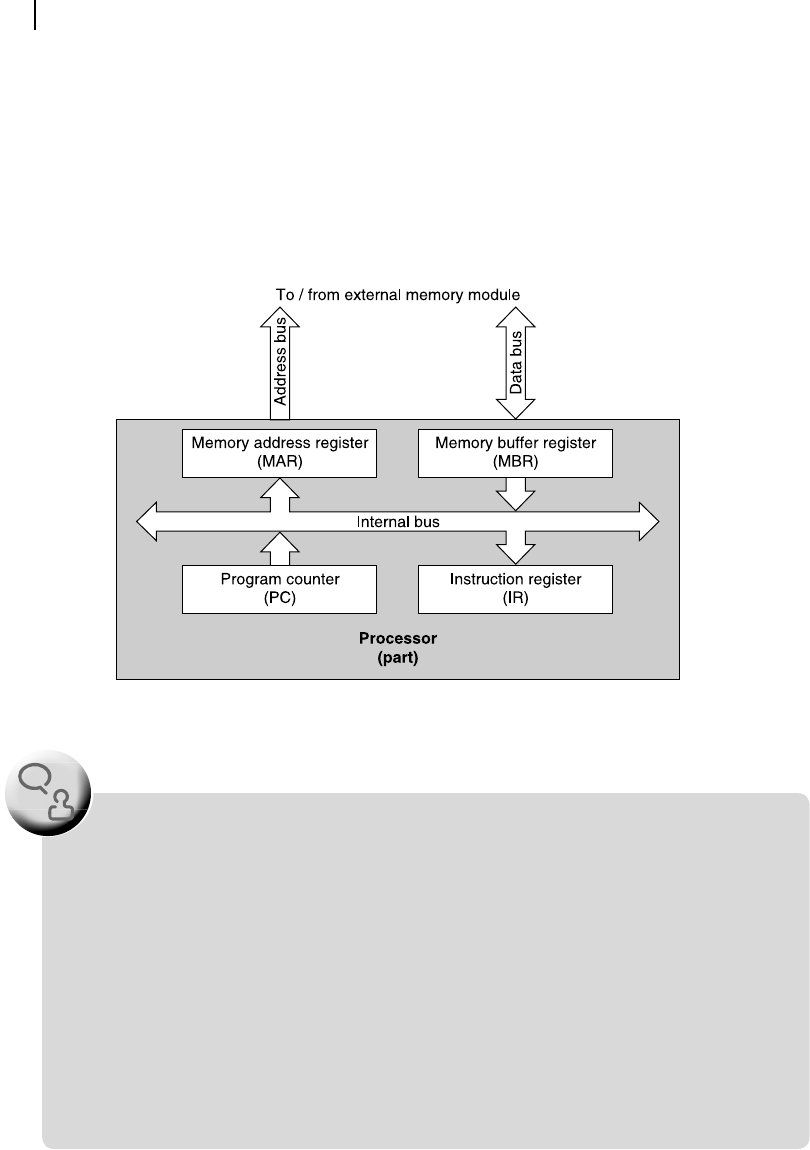
uses it for decoding and execution. The memory address register (MAR) holds the address of that loca-
tion of memory with which the processor is currently interested to communicate with. In other words,
MAR is directly connected with the address bus of the processor ( Figure 10.1 ). We know that through
this address bus, which is an external bus, the processor sends out signals to target one memory loca-
tion within the system memory area. Finally, the memory buffer register (MBR) is a register, connected
directly with the data bus of the processor to transact (read or write) data between processor and the
target memory location. Note that the opcode is rst received by this register and then transferred to the
IR. All important features of these four registers are presented in Table 10.1 .
Figure 10.1 Arrangement of registers for a fetch cycle
At this stage, the reader may ask a question that what is the utility of providing additional
registers like MAR or MBR for communicating address and data with external memory. As the
address would always be within PC and the instruction is always shifted to IR, why not PC and
IR are directly interfaced with external address bus and data bus, respectively?
As an answer, it may be pointed out that instruction fetching is not the only purpose of exter-
nal address and data bus. Many times other operands are also to be transacted through these
buses. For example, during subroutine calls the address of the next instruction to be saved over
stack-top through SP and the data within SP must then be available through external address
bus. Therefore, dedicated registers to accommodate external address and corresponding data
seem to be essential. Furthermore, at a later stage we shall see that when MAR is emitting
the external address, the PC is being simultaneously incremented by one for the next operation.
These types of parallel operations are not possible if PC is connected with external address bus.
F
O
O
D
F
O
R
T
H
O
U
G
H
T
M10_GHOS1557_01_SE_C10.indd 304M10_GHOS1557_01_SE_C10.indd 304 4/29/11 5:19 PM4/29/11 5:19 PM

Control Unit Operation 305
Register Name Content details Functioning
PC Program counter Address of next instruction Incremented by 1
MAR Memory address register Address of current instruction Copied from PC
MBR Memory buffer register Data buffer Data from/to data bus
IR Instruction register Opcode of current instruction Copied from MBR
Table 10.1 Functional details of PC, MAR, MBR and IR
To understand the mechanism of the fetch-cycle of the processor, we are to spend some more time
with Figure 10.1 . Note that there is an internal bus, which connects all four registers illustrated in
Figure 10.1 . Later in this chapter, we shall discuss more about this internal bus. Using this internal
bus, data is transferred from one register to another, within the processor. Note that all external
communication of the processor through address and data bus are implemented through MAR and
MBR exclusively. External control signals are also sent out through separate registers, not shown
in Figure 10.1 .
To start with, during any type of system reset (power-on or manual reset), the PC is initialized.
Content of the PC is then placed in MAR to fetch instruction code byte/word into MBR. At this stage a
memory read signal (control signal) is also generated and externally emitted by the processor, which is
not considered at present and it will be elaborated at a later stage in this chapter. The PC is incremented
by one and the data available within MBR is transferred to IR. After completion of its decoding and
execution of the instruction, the entire cycle is repeated. Therefore, we observe that the instruction fetch
operation is composed of several smaller steps which are designated as micro-steps . Given below are
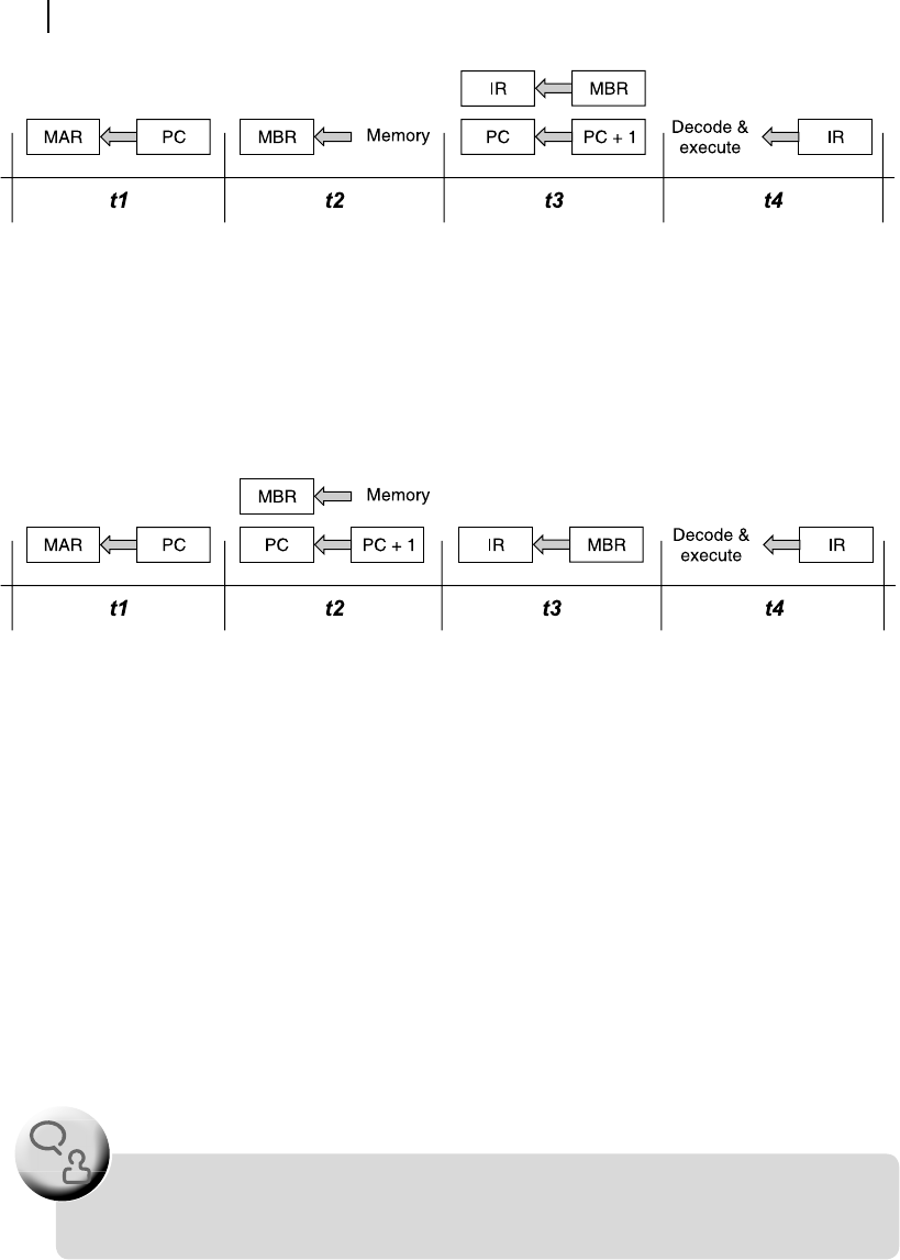
the necessary micro-steps of this process.
R Micro-step 1: Load MAR by content of PC.
R Micro-step 2: Receive data from memory to MBR.
R Micro-step 3: Transfer data received by MBR to IR.
R Micro-step 4: Increment PC by one.
R Micro-step 5: Decode and execute instruction.
R Micro-step 6: Repeat from Step 1.
It may be noted that Step 3 and Step 4 may be combined as these two actions are not dependent
upon each other. In the CU design, the designer must be careful about the sequence, which must
be properly maintained. For example, Step 1 and Step 4 cannot be executed simultaneously as they
are not independent with respect to each other. Graphically, these sequences are presented through
Figure 10.2 . From this illustration we may observe that four time-slices are necessary to complete
the whole task and the cycle is repeated, thereafter. Note that we are yet to consider or discuss about
two important details. One is the need of necessary control signals and their sequence. The second
is the fetching details of additional operands, if necessary for any particular instruction. We shall
discuss both of these aspect in following paragraphs. However, before that let us quickly discuss
another aspect, related with sequencing.
In Figure 10.3 , an alternate sequence of the fetch-cycle is depicted, which performs the same duty as
that illustrated in Figure 10.2 but in a different sequence. If we compare this with Figure 10.2 , then we
nd that, instead of incrementing PC (by one) during t3 , it is carried out during t2 . Now the question is,
M10_GHOS1557_01_SE_C10.indd 305M10_GHOS1557_01_SE_C10.indd 305 4/29/11 5:19 PM4/29/11 5:19 PM
306 Computer Architecture and Organization
which one is correct? As a matter of fact, both are correct, as this alternate sequence serves all purposes
perfectly, just like the previous sequencing. Only the grouping of micro-operations has changed. There-
fore, the reader may ask a question at this stage, is it allowed to group microinstructions in whichever
way we feel?
The reader should note that the time slices shown in Figure 10.2 and 10.3 may vary in length
depending upon the instruction to be handled.
F
O
O
D
F
O
R
T
H
O
U
G
H
T
Figure 10.3 An alternate sequence of fetch-cycle of a processor
The answer is ‘ no, we cannot ’. To group micro-operations, we have to be careful to check two
important aspects. First, the proper sequence must be maintained by grouping of the micro-operations.
In no case an eventual grouping may be allowed to alter the desired sequence of micro-operations. For
example, if we place MBR-loading micro-operation in t1 and MAR-loading micro-operation in t2 , it
would not be the correct sequence that we are targeting for. Second, all types of con icting grouping
must be avoided. It means that the types of micro-operations which need time-wise separation should
not be placed within the same time-slice. For example, loading MBR from memory and loading IR
from MBR should not be placed within the same time-slice. Why? This is because loading MBR from
memory needs some nite amount of time and, therefore, simultaneously IR cannot be loaded by a cor-
rect data from MBR. Therefore, in short, transaction of same data two times in the same time-slice is
not permitted.
Figure 10.2 Sequence of fetch-cycle of a processor
M10_GHOS1557_01_SE_C10.indd 306M10_GHOS1557_01_SE_C10.indd 306 4/29/11 5:19 PM4/29/11 5:19 PM

Control Unit Operation 307
10.3.2 Indirect Cycle (Operand Fetch)
Not for all but for some instructions there might be a necessity to fetch the related operand(s) from
memory. It is needless to mention that this would be a special type of cycle, different from the familiar
fetch-cycle and we designate this type of cycles as indirect cycle . Here, the addressing mode (Section
6.4) would play an important part. To refresh the memory of the reader it may be indicated, here, that
for immediate addressing mode, data would be a part of the instruction itself, which may only be under-
stood after decoding the instruction. For direct addressing mode, the address of the target data would
be a part of the instruction. Other addressing modes would target the data as explained in Chapter 6.
For the purpose of explanation, we represent all other remaining addressing modes by indirect address-
ing mode. The functioning of any indirect cycle would be different in immediate, direct and indirect
addressing modes, which we shall now discuss separately.
In the case of immediate addressing mode (data being a part of the instruction itself), the MAR is
loaded by PC in t1 and the immediate data from memory is brought to MBR during t2 . The PC is incre-
mented by one as usual during t2 . However, generally the immediate operand (data) is sent to one of the
registers related with ALU for further operations as per the instruction.
When the indirect cycle is to deal with direct addressing mode, MAR is loaded by PC during t1 and
the corresponding memory output, received within MBR (during t2 ) is transferred to MAR (during t3 )
to get the data from memory to MBR during t4 . This data from MBR are then transferred to its desired
location, generally, to one of the ALU registers.
Finally, during indirect addressing mode, one more operation is required with respect to direct
addressing mode to get the address itself from another address. Therefore, the number of machine
cycles, or in other words, the time required would be more in such a case of indirect addressing.
People say that exception proves the rule and in this present case also there may be some
exceptions. The reader may refer Solved Example 4 of Section 10.6.4, where for the 3-Bus
system the ALU result is allowed to be communicated to general purpose register R2 through
the result register Z. However, these are very special occasions and the general rule is not to
merge two time-slices together.
F
O
O
D
F
O
R
T
H
O
U
G
H
T
Because more time is necessary for implementing complex addressing modes, therefore, RISC
processors try to maintain allowable addressing modes as simple as possible. This point was
mentioned in Chapter 5. However, the reason behind it becomes more clear when we study
the processor at micro-architecture level.
F
O
O
D
F
O
R
T
H
O
U
G
H
T
M10_GHOS1557_01_SE_C10.indd 307M10_GHOS1557_01_SE_C10.indd 307 4/29/11 5:19 PM4/29/11 5:19 PM
..................Content has been hidden....................
You can't read the all page of ebook, please click here login for view all page.