

316 Computer Architecture and Organization
To conclude, we should try to visualize that for any processor the number of parameters is many
more than our example case and the complexity of the Boolean expressions also increases at the same
rate. Therefore, although hardwired controlled units make the processor work faster, it is generally
avoided in CISC processors. For RISC processors, as the number of instructions is minimal, the hard-
wired control units are adopted by several processors.
10.6 SOLVED EXAMPLES
In Section 9.9 of Chapter 9, we have discussed about some example cases on data path design. There, we
have indicated that discussions related to the necessary control signals would be taken up in this chapter. It
is reaf rmed here that there is no established standard method existing either for data path or for CU design
procedure, and every processor may be taken as an exceptional case. However, in this section we shall dis-
cuss about some elementary design issues related to few examples, which had been initiated in Section 9.9.
10.6.1 Example 1 (Using C-Bus)
Problem
Assuming that a processor was planned with one data path (C-Bus) only, design the control signals to fetch
the next instruction from external memory location. Assume that the instruction is of one byte only. After
fetching, the instruction should be available within the IR and PC must be incremented by one.
Solution
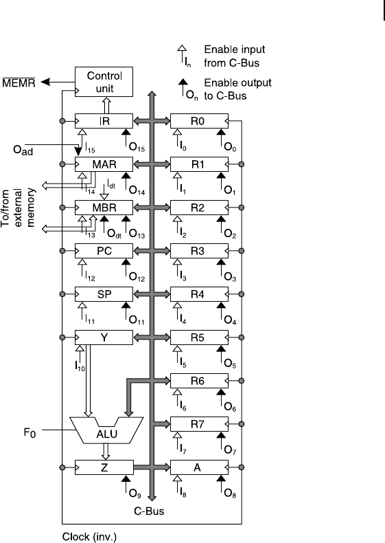
We have reproduced Figure 9.19 of Chapter 9 as Figure 10.9 here with some necessary modi cations.
However, we should clarify at this juncture that there are a total of two registers to communicate with
external memory. These two registers are memory address register (MAR) and memory buffer register
(MBR) as shown in Figure 10.9 . In our example case, we are assuming that for the purpose of instruc-
tion fetch the address available in PC would be copied to MAR and emitted to external memory address
bus by MAR (Table 10.1 for descriptions and functions). The instruction byte would be available from
external memory into the MBR and then would be copied to IR. To get any operand, MAR would gener-
ate the address and MBR would receive the data. In our present example we are not going to use MAR
and MBR for operand fetch and only two registers namely PC and IR would be used to hold starting and
completion information (address and instruction byte, respectively). The related micro-operation steps
and their control signals’ sequences should be as follows:
R Step 1: Copy PC to MAR using C-Bus.
R Step 2: Allow MAR to be available in external address bus and assert memory read signal
(MEMR) low and maintain it as low for one complete clock cycle. Latch the instruction byte
available at MBR and then make memory read signal (MEMR) high again.
R Step 3: Copy MBR into IR using C-Bus.
R Step 4: Send content of PC to ALU through C-Bus, setting it at increment-by-one mode by keep-
ing F0 low. Latch incremented value from ALU (result) within Z
R Step 5: Copy Z to PC using C-Bus.
In Chapter 9, we have described how the system clock signal may be used after inversion to gener-
ate the falling edge (↓) to latch data inside registers. The same technique we would implement here.
All register enabling signals are also assumed to be active low. We shall now discuss each step of the
operation with necessary details.
M10_GHOS1557_01_SE_C10.indd 316M10_GHOS1557_01_SE_C10.indd 316 4/29/11 5:19 PM4/29/11 5:19 PM
Control Unit Operation 317
In Figure 10.9 , the reader’s attention is drawn to the fact that for most of the registers C-Bus inter-
facing is bidirectional and, therefore, these registers have two control signals, one for sending its data
out through C-Bus and another is for receiving external data through C-Bus. These control signals for
registers are indicated as I
n
and O
n
in Figure 10.9 . Only the following registers are exceptional and need
special attention in this case.
Register Z only outputs data and input is always from ALU. It has only one control signal O
9
for allow-
ing its data out to C-Bus. Similarly, Y register always receives data from C-Bus through the control signal
I
10
. Output from Y register is always available immediately to ALU. The content of IR is always available
to the CU. Apart from C-Bus connection, register MAR is also connected with external address bus. The
content of MAR is available in external address bus as long as the corresponding control signal O
ad
is low.
As MBR has to communicate with external data bus, two additional control signals are provided for this
register, namely I
dt
and O
dt
to allow input and output related with external data bus.
Figure 10.9 Control signals necessary for instruction fetch
M10_GHOS1557_01_SE_C10.indd 317M10_GHOS1557_01_SE_C10.indd 317 4/29/11 5:19 PM4/29/11 5:19 PM

318 Computer Architecture and Organization
The reader is reminded here that at the time of nalization of micro-operational steps, the number of
data paths available within the processor plays a vital role. For the present problem, we are restricted
with one data path only. However, in later examples we shall solve the same problem using more num-
ber of data paths and the difference in micro-operational steps would be emphasized. We shall observe
later that the total time consumed by the necessary micro-operations would be substantially less if more
data paths are available to the control unit.
Step 1
To copy PC to MAR through the C-Bus both PC output enable control and MAR input enable control
signals have to be reset as low for one clock period after which they may be brought back to their origi-
nal high state. This has to be implemented from one falling edge to next falling edge of the system clock.
The in-between rising edge of the clock would be used (after inversion) to latch the data from PC into
MAR. Timing diagram for this step is illustrated in Figure 10.10 .
Figure 10.10 Timing diagram for copying PC to MAR
Step 2
The next step is to allow MAR content in the external address bus and maintain MEMR low for one
complete clock cycle, from one falling edge to next falling edge. At the same time MBR also has to be
allowed to accept data from external data bus. The data (instruction byte) available in MBR are to be
latched by the falling edge of inverted clock signal. This is illustrated through Figure 10.11 . Note that
two different external data paths are being used for these two communications, one for address and
another for data.
It was already indicated that for communicating with external address and data bus registers MAR
and MBR are provided with additional control signals. As the external address bus is always unidirec-
tional, only one extra control signal for MAR that is O
ad
is provided. However, the external data bus is
bi-directional and, therefore, it needs two additional control signals for communicating with the data
bus. These two additional control signals of MBR are designated as I
dt
and O
dt
. For the present problem,
we shall use I
dt
to allow data from external memory into MBR through external data bus.
Step 3
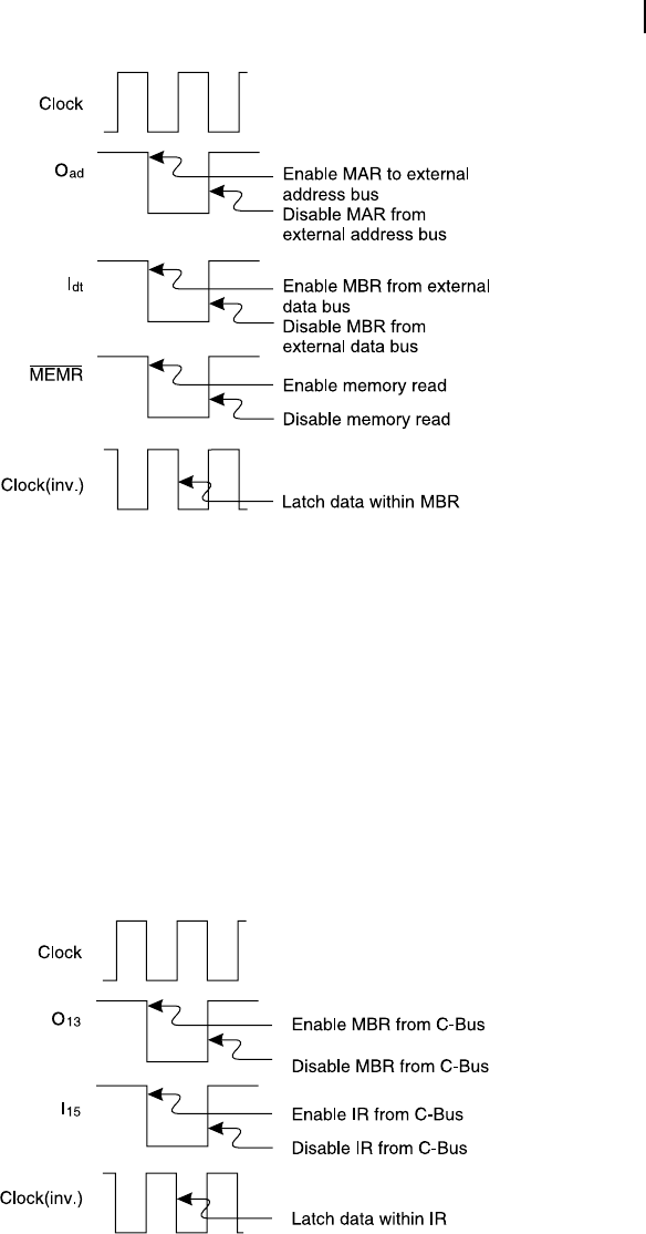
In the next step, the data (instruction byte) available in MBR have to be copied to IR. C-Bus has to be used for
this copy operation and another complete clock cycle is necessary, as shown in Figure 10.12 . By maintaining
M10_GHOS1557_01_SE_C10.indd 318M10_GHOS1557_01_SE_C10.indd 318 4/29/11 5:19 PM4/29/11 5:19 PM
Control Unit Operation 319
O 13 low, MBR output is connected with C-Bus. To allow data from C-Bus within IR, the control signal I15
has to be asserted low. Latching data available within IR would be done by the inverted clock signal.
Step 4
To increment PC by one, next duty is to send the content of PC to ALU through C-Bus. The ALU has
to be con gured for increment by one mode by making its function select input (F0) low. Note that this
operation of ALU accepts only one operand and the content of Y register does not affect the result. We
assume that the ALU is a static one and the result of operation is assumed to be immediately available
within its result register Z. The related timing diagram for this operation is shown in Figure 10.13 .
Step 5
The nal step is to copy the content of Z register into PC through the C-Bus. This is to be done by
enabling Z register to output its data in C-Bus and simultaneously enabling PC to receive data from
Figure 10.11 Timing diagram for reading from external memory using MAR and MBR
Figure 10.12 Timing diagram for copying MBR into IR
M10_GHOS1557_01_SE_C10.indd 319M10_GHOS1557_01_SE_C10.indd 319 4/29/11 5:19 PM4/29/11 5:19 PM

320 Computer Architecture and Organization
Figure 10.14 Timing diagram for copying Z to PC
C-Bus. The falling edge of inverted clock signal would latch the data (incremented value of PC by 1)
within PC. This phase of the related timing diagram is shown in Figure 10.14 .
We now present the complete timing diagram of the whole operation of fetching the instruction in
Figure 10.15 . With only one data path available (C-Bus) the total number of cycles required to complete
the whole operation would need ve cycles, as we may observe from Figure 10.15 . Note that the signal
O
12
is duplicated just for the sake of clarity.
At this stage, the reader may ask a question that whether it would be desirable to merge Cycle 2 and
Cycle 3 as one cycle. Apparently, there is no harm in implementing it as three separate micro-operations
To be very precise, even for a static ALU, there would be some delay because of the set-up
time and hold time. At present, we are not considering these details.
F
O
O
D
F
O
R
T
H
O
U
G
H
T
Figure 10.13 Timing diagram for incrementing PC by one through ALU
to
Z
M10_GHOS1557_01_SE_C10.indd 320M10_GHOS1557_01_SE_C10.indd 320 4/29/11 5:19 PM4/29/11 5:19 PM
..................Content has been hidden....................
You can't read the all page of ebook, please click here login for view all page.