
Control Unit Operation 321
would be using three separate paths. The rst path is the external address line, the second path is the
external data paths and the third one is the internal C-Bus.
However, the design would not be an excellent one if we do so. The reason is that, in that case, the
external memory location would be directly connected with the instruction register IR through the
memory buffer register MBR. It is undesirable to use a register as a transparent buffer interconnecting
external devices and may initiate other complications. The standard practice in this case is to shift the
data from one point (location or register) to another point in one clock cycle.
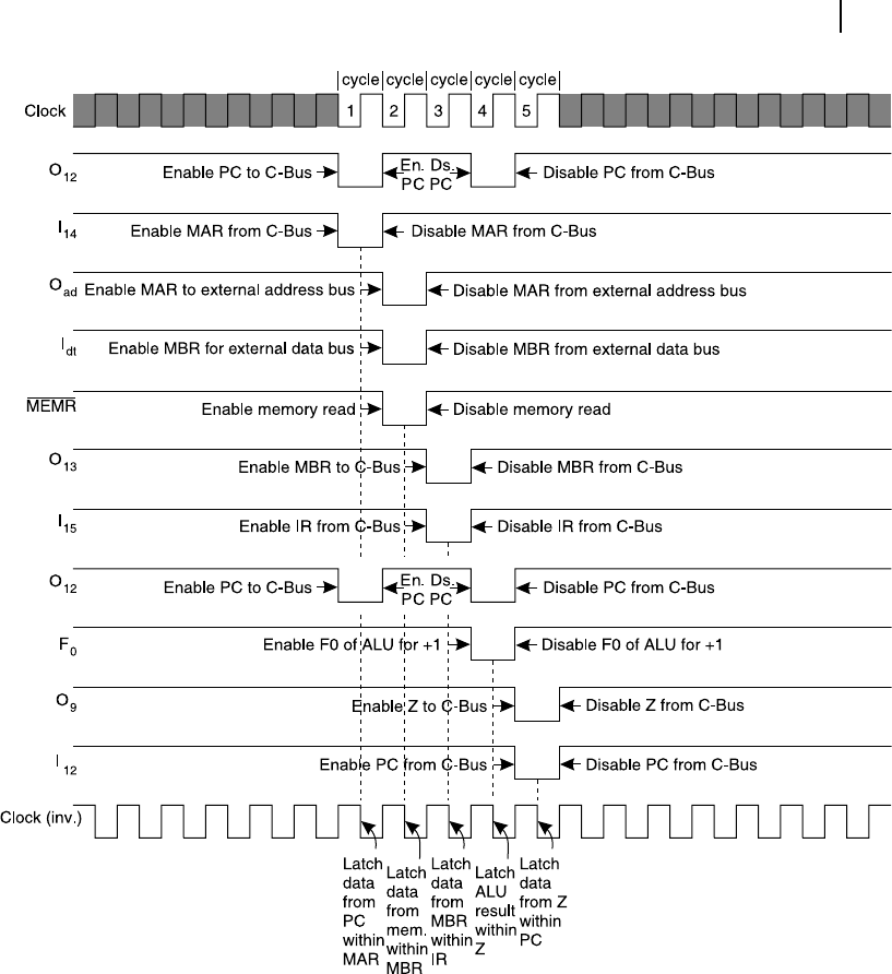
Figure 10.15 Complete timing diagram for instruction fetch using C-Bus
M10_GHOS1557_01_SE_C10.indd 321M10_GHOS1557_01_SE_C10.indd 321 4/29/11 5:19 PM4/29/11 5:19 PM

322 Computer Architecture and Organization
Cycle O
12
I
14
O
ad
I
dt
MEMR O
13
I
15
F
0
O
9
I
12
Operation
1 0 0 1 1 1 1 1 1 1 1 Copy PC to MAR
2 1 1 0 0 0 1 1 1 1 1 Fetch instruction
3 1 1 1 1 1 0 0 1 1 1 Copy MBR to IR
4 0 1 1 1 1 1 1 0 1 1 PC to ALU
5 1 1 1 1 1 1 1 1 0 0 Z to PC
Table 10.2 Control Signals for Micro-operation with C-Bus
Out of these ve operational cycles the C-Bus is being used in four cycles, namely rst, third, fourth
and fth cycle. The last three cycles may be merged to lesser number of cycles if more data paths are
available.
If the system is implemented with a micro-coded ROM for generating the control signals, then the con-
tent of that ROM for related signals and related operations would be similar to that presented in Table 10.2 .
10.6.2 Example 2 (Using C-Bus and B-Bus)
Problem
Solve the previous problem assuming that two data paths are available, i.e., C-Bus and B-Bus.
Solution
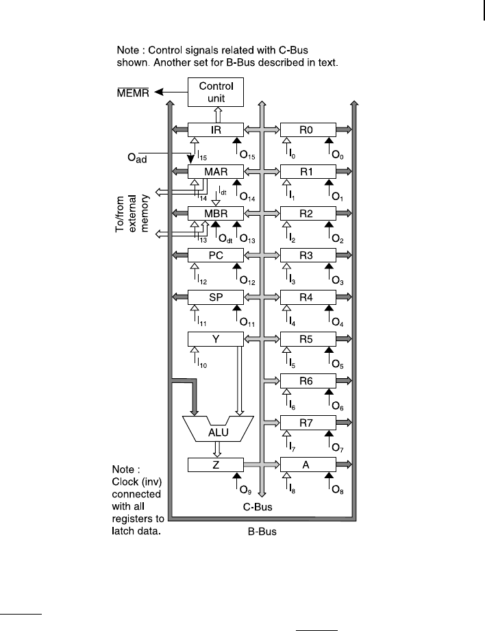
In Chapter 9, we have introduced processors with two data paths, namely C-Bus and B-Bus. In Figure 10.16 ,
a similar architecture is illustrated with some control signals required for the C-Bus. Although another set of
similar control signals are available for the B-Bus interface with all registers (except Y and Z), for maintain-
ing the clarity of illustration, these additional control signals are not shown in Figure 10.16 . In the following
text, names of control signals like I
0
or O
0
(example case for register R0) should be taken for C-Bus control,
while control signals indicated as I’
0
or O’
0
should be be taken as B-Bus related control signals for the same
register. Just like the previous example, all control signals are assumed to be active low. Therefore, when
I’
0
goes low, register R0 would receive input from B-Bus and when I
0
goes low, it would receive input from
C-Bus. Similarly, a low in O’
0
would place the data of R0 in B-Bus and a low in O
0
would place the data
within R0 in C-Bus.
In general, all registers are bidirectionally connected with both C-Bus and B-Bus except Y and Z
registers of ALU. The Z register receives the result of the static ALU directly and can only output the
data into C-Bus. Z register is not connected with B-Bus. Y register may receive input only from C-Bus
and its content is directly available as one of the two inputs of the ALU. Y register is also not connected
with the B-Bus.
MAR has a third bus for external address transmission and it is controlled by O
ad
control signal, like
the previous example. The address bus is unidirectional and can only receive data from MAR. MBR is
bidirectionally interfaced with external data bus and has two control signals for this purpose. If I
dt
is low,
MBR receives data from external data bus. If O
dt
is low, MBR outputs data to external data bus. Finally,
all registers are connected with inverted clock signal (not shown in Figure 10.16 ) for input latching,
similar to the previous example.
In the last example, we have solved the problem in ve steps using only one data path. As we are
now allowed to use two data paths, following four steps are suf cient to solve the problem. By compar-
ing these steps with those of previous example, the reader may observe that Steps 3 and 4 of previous
example are merged as Step 3 in the present example, converting the last step as Step 4.
M10_GHOS1557_01_SE_C10.indd 322M10_GHOS1557_01_SE_C10.indd 322 4/29/11 5:19 PM4/29/11 5:19 PM
Control Unit Operation 323
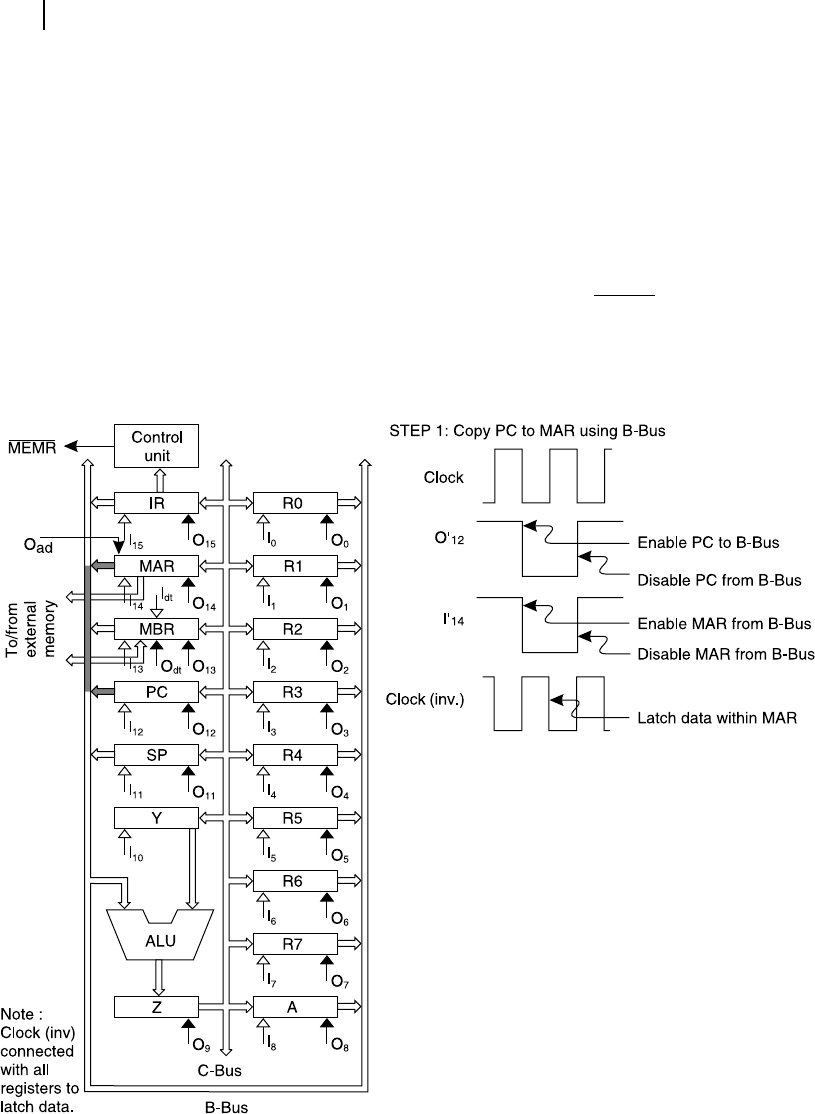
R Step 1: Copy PC to MAR using B-Bus.
R Step 2: Allow MAR to be available in external address bus and assert memory read signal
(MEMR) low and maintain it as low for one complete clock cycle. Latch the instruction byte
available at MBR and then make memory read signal (MEMR) high again.
R Step 3: Copy MBR into IR using C-Bus. Send content of PC to ALU through B-Bus, setting it at
increment-by-one mode by keeping F0 low. Latch incremented value from ALU (result) within
Z. Note that IR and Z would be latched simultaneously.
R Step 4: Copy Z to PC using C-Bus.
We now discuss about each step of the operation in details. In the last example, we have explained
each of the steps with the related timing diagram. As there was only one bus (C-Bus) in the last example,
data- ow visualization was not a problem. However, as we are using a pair of data paths in this example
(C-Bus and B-Bus), apart from timing diagram, the related data ow is also illustrated in these cases.
Figure 10.16 Control signals necessary for instruction fetch
only, are
M10_GHOS1557_01_SE_C10.indd 323M10_GHOS1557_01_SE_C10.indd 323 4/29/11 5:19 PM4/29/11 5:19 PM
324 Computer Architecture and Organization
Step 1
During the rst clock cycle, PC is copied to MAR by enabling two control signals, namely O’
12
and
I’
14
. The rst control signal, when it goes low, would enable PC contents to be available in B-Bus
( Figure 10.17 ). The next control signal would enable the input buffer of MAR and allow the data from
B-Bus to be available within it. As usual, the inverted clock signal would latch this data within MAR.
The data path used in this cycle is heavily shaded in Figure 10.17 .
Step 2
The next clock cycle has to be used to get the opcode byte from external memory. In this case, we use same
signals and follow the same sequence as that of the previous example. By making the control signal O
ad
low,
the content of MAR is placed on the external address bus and at the same time MEMR is also held low. This
operation enables external memory device to send the required data through the external data bus.
To accept this data, I
dt
control signal related with MBR is maintained low ( Figure 10.18 ) and the data from
memory within MBR is latched by the inverted clock signal, which was elaborated in the previous example.
Figure 10.17 Timing diagram and data flow for Step 1
M10_GHOS1557_01_SE_C10.indd 324M10_GHOS1557_01_SE_C10.indd 324 4/29/11 5:19 PM4/29/11 5:19 PM

Control Unit Operation 325
Figure 10.18 Timing diagram and data flow for Step 2
At this stage the reader may ask a question that as we are not using any internal data paths,
what is the harm in sending the PC content to the ALU for the purpose of incrementing it by
one. In that case, the next cycle may be used for transporting MBR content within IR through
B-Bus as well as transporting Z register content to PC, using C-Bus and finishing the whole
operation in just three cycles instead of four.
As a reply to this question, we may clearly say that there is absolutely no harm in imple-
menting the scheme and, indeed, in that case, the operation may be completed within three
cycles instead of four. However, like all design problems there are multiple methods to solve it
and we shall discuss about the three-cycled operation in the next example.
F
O
O
D
F
O
R
T
H
O
U
G
H
T
M10_GHOS1557_01_SE_C10.indd 325M10_GHOS1557_01_SE_C10.indd 325 4/29/11 5:19 PM4/29/11 5:19 PM
..................Content has been hidden....................
You can't read the all page of ebook, please click here login for view all page.