

326 Computer Architecture and Organization
After the operation, both O
ad
as well as I
dt
are brought back to high state, as indicated in the timing diagram.
The external address and data bus used in this cycle for data ow are heavily shaded for indication. External
memory read signal MEMR is also brought back to its original high state at the end of the present clock cycle.
Step 3
At this stage, two more operations are pending. The rst one is to copy the data within MBR into IR and
the second one is to increment PC by one. In our Step 3, we copy MBR to IR using C-Bus and enable
PC to ALU through B-Bus. The F0 function, input of ALU is held low so that increment by one function
of ALU may be implemented. Note that the falling edge of inverted clock would simultaneously latch
two sets of data within two different registers in this case. One is IR and the second is Z register of ALU.
Therefore, to implement this cycle, MBR is enabled to output through C-Bus by making its control
signal O
13
low. At the same time the control signal I
15
, which enables input from C-Bus to IR, is also kept
low. This ensures a data ow from MBR to IR through C-Bus and the rest is carried out by the latching
signal, the inverted clock.
To complete the other operation during the same cycle, we use another bus, which is presently free,
i.e., the B-Bus. The PC content is allowed to reach ALU by making the related control signal of PC, i.e.,
O’
12
low. The function input signal of ALU (F0) is also maintained low so that the ALU may perform
the increment by one operation. The result is available within Z register of ALU, which is latched by the
Figure 10.19 Timing diagram and data flow for Step 3
M10_GHOS1557_01_SE_C10.indd 326M10_GHOS1557_01_SE_C10.indd 326 4/29/11 5:19 PM4/29/11 5:19 PM

Control Unit Operation 327
inverted clock signal (not shown in Figure 10.19 ), and at the same time, as latching data within IR. In
Figure 10.19 , the shaded portion of data paths are used by the data ow during this clock cycle.
Step 4
In the nal cycle, i.e., the fourth cycle, we copy the content of Z register (incremented value of PC) to
PC. In this case, C-Bus is used as it is customary to use the C-Bus for transporting the result of ALU
operation. The cycle begins by asserting O
9
low and, thus, enabling Z to output its data within the
C-Bus. At the same time, I
12
of PC is also maintained low so that PC may accept data from C-Bus, as
shown in Figure 10.20 . The inverted clock is used to latch the data within PC and the whole operation is
over. The heavily shaded data path in Figure 10.20 indicates the data ow for the present cycle.
The advantage of an extra data path should be clear to the reader from this example, which shows
that the processor would be able to execute faster with multiple data paths. In the case of designing for
multiple data paths the designer must keep in mind that the same data path cannot transport two dif-
ferent set of signals at the same time . In certain cases, the direction of data ow is also restricted, for
example the Z register, in the case of C-Bus of the present problem, where data is allowed to move out
Figure 10.20 Timing diagram and data flow for Step 4
M10_GHOS1557_01_SE_C10.indd 327M10_GHOS1557_01_SE_C10.indd 327 4/29/11 5:19 PM4/29/11 5:19 PM
328 Computer Architecture and Organization
from Z but not allowed to move in. The next important point is to maintain the sequence of operation,
if one is dependent upon another. For example the PC cannot be incremented in our example unless it
is copied in MAR.
Another assumption should be cleared at this stage that fetching the opcode byte is the initial duty of
the CU to execute every instruction. However, this duty is not over by placing the opcode byte within
IR. As a matter of fact, the execution of the CU just begins from this stage and multiple additional cycles
in Z
Figure 10.21 Complete timing diagram for instruction fetch using C-Bus and B-Bus
M10_GHOS1557_01_SE_C10.indd 328M10_GHOS1557_01_SE_C10.indd 328 4/29/11 5:19 PM4/29/11 5:19 PM

Control Unit Operation 329
are necessary to complete the ongoing instruction before fetching the next instruction. We have taken up
only this part of operation for the purpose of explaining some details related with data path and control
signal design.
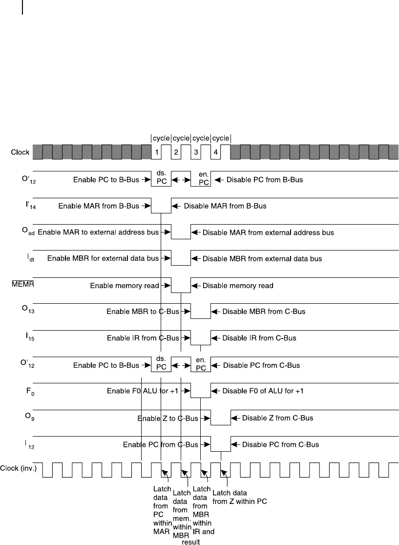
The complete timing diagram for the present operational example is illustrated in Figure 10.21 .
As we can see, it would consume four clock cycles and with alternate design methods it may further
be reduced to three cycles. In this timing diagram of Figure 10.21 , the reader may note that the signal
O’
12
is depicted at two different places although it is the same signal. This has been done just for better
understanding of the sequences.
If any software micro-coding is necessary, control signals related with this example may be gener-
ated as per the details available in Table 10.3 . In Table 10.3 , the reader should note that the control signal
O’
12
is listed only once, and in two cycles, Cycle 1 and Cycle 3, it goes low. We shall now redesign
control signals to further optimize the number of cycles.
Cycle O’
12
I’
14
O
ad
I
dt
MEMR O
13
I
15
F
0
O
9
I
12
Operation
1 0 0 1 1 1 1 1 1 1 1 Copy PC to MAR
2 1 1 0 0 0 1 1 1 1 1 Fetch instruction
3 0 1 1 1 1 0 0 0 1 1 Copy MBR to IR and PC to ALU
4 1 1 1 1 1 1 1 1 0 0 Z to PC
Table 10.3 Control signals for micro-operation with C-Bus and B-Bus
10.6.3 Example 3 (Alternate Solution Using C-Bus and B-Bus)
Problem
Solve the same problem with reduced number of required cycles.
Solution
When we are having two independent buses, the operations may be carefully planned to minimize the
bus-cycles of the processor. For the instruction fetch problem, the following may be the necessary steps.
R Step 1: Copy PC to MAR through C-Bus and simultaneously send PC to ALU using B-Bus. Set
ALU in increment by one mode by turning F0 low. Latch data in MAR and also the result in Z
simultaneously.
R Step 2: Allow MAR to send address via external address bus and also make MEMR low. Receive
data from external memory through external data bus at MBR and latch the data. Simultane-
ously, copy result from Z to PC using C-Bus and latch the data inside PC.
R Step 3: Copy MBR to IR through C-Bus and latch the data within IR.
Control signals related with this operation are presented in Table 10.4 .
Therefore, we can conclude that instead of four cycles as in Example 2, the operation may be com-
pleted within three cycles as illustrated above. Note that we are using B-Bus simultaneously with C-Bus
in one cycle only as in previous example. For all remaining cycles, we are using C-Bus. As a matter of
fact, an additional data path would not enhance the ef ciency in this situation. The reader may ask why
or when a three-data-path system is adopted? In general, three data paths are properly utilized in the case
of ALU operations, which we are about to discuss now.
M10_GHOS1557_01_SE_C10.indd 329M10_GHOS1557_01_SE_C10.indd 329 4/29/11 5:19 PM4/29/11 5:19 PM

330 Computer Architecture and Organization
Register Control signal Input/Output Bus
PC O
12
Output to C-Bus
PC O’
12
Output to B-Bus
PC I
12
Input from C-Bus
MAR I
14
Input from C-Bus
MAR O
ad
Output to Address bus
MBR I
dt
Input from Data bus
MBR O
13
Output to C-Bus
ZO
9
Output to C-Bus
IR I
15
Input from C-Bus
Table 10.4 Description of relevant control signals
10.6.4 Example 4 (ALU Operation Using 1-Bus and 3-Bus)
In the last example, we have demonstrated that using the 2-Bus structure the speed of execution may be
considerably enhanced with respect to 1-Bus system. Therefore, it may not be incorrect to assume that
incorporating another data path with the system would further enhance the system performance. The
real advantage of 3-Bus structure becomes evident when we encounter the ALU operation. The follow-
ing problem is a comparison between 1- and 3-Bus structures related with ALU operation only.
Problem
Compare the performance of 1- and 3-Bus systems for ALU operation using an example instruction of
adding two operands present in two CPU registers and storing the result of the operation in a third register.
Solution
We have already indicated that buses A-, B- and C- are related with ALU and, generally, C-Bus is related
with the result register, which in our example case is the Z register. Figure 10.22 illustrates the three-bus
system, which we have already discussed in Chapter 9.
For the present problem, we assume that R0 and R1 are the two registers, which are having the
operands to be added together. We also assume that the result of this addition needs to be placed in R2
register. For the purpose of clarity, only the relevant control signals are illustrated in Figure 10.22 . The
whole operation may be completed in one cycle if following method is used.
R Step 1: Allow R0 to be available to the ALU through A-Bus by making O”
0
low. Simultane-
ously, allow R1 to be available to the ALU using B-Bus by making O’
1
low. Set ALU in add
two operands mode by activating proper control signal F1 as low. Allow Z register to output its
content within C-Bus by making O
9
low and allow register R2 to receive data from C-Bus by
making I2 low. The result of addition would be simultaneously latched within Z and R2 by the
inverted system clock.
Therefore, we can conclude that the whole operation of adding two operands in two registers through
ALU and placing its result in a third register demands only one cycle if three independent data paths are
provided. Also note that, in this case, we are using all three data paths simultaneously throughout the
cycle. In Figure 10.22 , the relevant portion of these data paths are heavily shaded. Let us now observe
M10_GHOS1557_01_SE_C10.indd 330M10_GHOS1557_01_SE_C10.indd 330 4/29/11 5:19 PM4/29/11 5:19 PM
..................Content has been hidden....................
You can't read the all page of ebook, please click here login for view all page.