
336 Computer Architecture and Organization
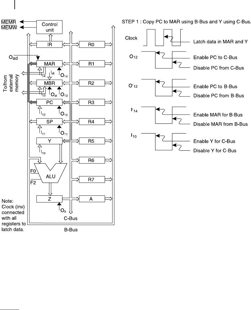
simultaneously used to copy PC into Y. Note that alternately only C-Bus may also be used to copy PC
into both MAR and Y. PC is enabled for both data paths. MAR as well as Y are enabled to accept data
from respective buses. Data ow paths and timing diagrams of related control signals are shown in
Figure 10.26 .
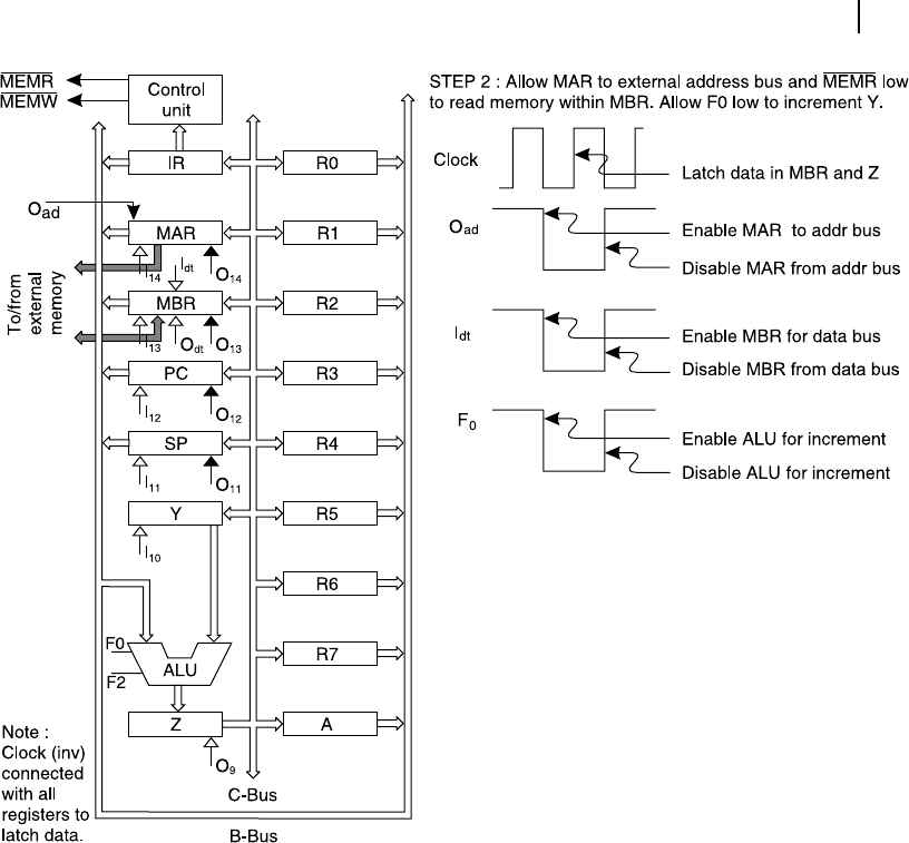
Step 2
As the second step, MAR is enabled to send its content through external address bus along with enabled
MEMR signal. The data from external memory is received within MBR. Note that this is the address of
the subroutine being called by the ongoing instruction.
During the same cycle the latched value of PC in Y is incremented by one through ALU by
enabling its function input F0. The incremented value is latched within Z register. Note that this
value is the return address to be saved on stack-top through current value in SP. This would be taken
Figure 10.26 Data flow and timing diagram for Step 1
M10_GHOS1557_01_SE_C10.indd 336M10_GHOS1557_01_SE_C10.indd 336 4/29/11 5:20 PM4/29/11 5:20 PM
Control Unit Operation 337
care of in subsequent cycles. Timing diagram and data ow representation for this cycle is illustrated
in Figure 10.27 .
Step 3
In Step 3, two separate copy operations are performed simultaneously. The data received from external
memory in the last cycle within MBR is copied to PC through B-Bus. PC now has the address of the
subroutine being called.
At the same time, within the same cycle content of SP is copied into MAR through C-Bus. Therefore,
MAR is loaded with the address of the stack-top, where the return address has to be saved. This return
address is already latched within Z, which is the result register of ALU. Figure 10.28 shows the timing
diagram and paths followed by data for this cycle.
Figure 10.27 Data flow and timing diagram for Step 2
M10_GHOS1557_01_SE_C10.indd 337M10_GHOS1557_01_SE_C10.indd 337 4/29/11 5:20 PM4/29/11 5:20 PM

338 Computer Architecture and Organization
Figure 10.28 Data flow and timing diagram for Step 3
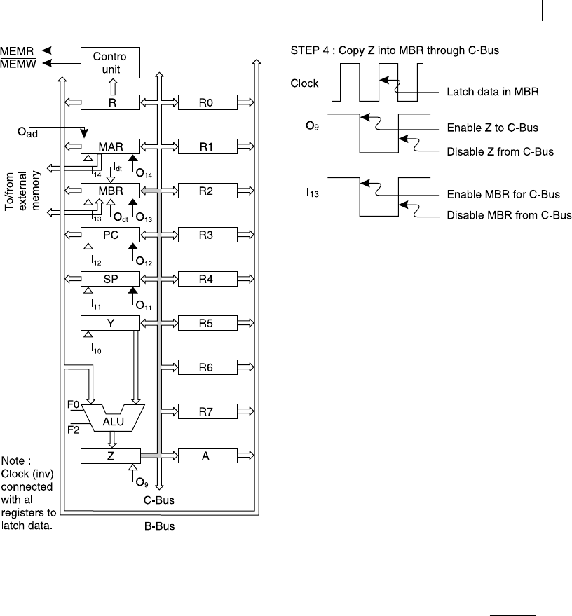
Step 4
In the rst cycle itself (of this example), the content of PC was copied into Y register of ALU. In the
second cycle, the ALU was set to increment this value in Y by one and store within the result register Z.
As a matter of fact, this is the return address to be stored over stack-top pointed by SP.
Therefore, in the present cycle content of Z is copied to MBR using C-Bus. The path of data ow for
this operation and related timing diagram are shown in Figure 10.29 .
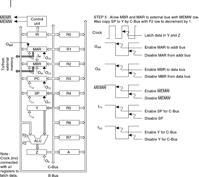
Step 5
The return address was already calculated by incrementing PC by one in Step 2. This incremented value
of PC was copied from Z register to MBR in Step 4. The address of stack-top was copied from SP to
MAR in Step 3. Therefore, in this cycle the return address within MBR is stored on stack-top pointed
M10_GHOS1557_01_SE_C10.indd 338M10_GHOS1557_01_SE_C10.indd 338 4/29/11 5:20 PM4/29/11 5:20 PM
Control Unit Operation 339
Figure 10.29 Data flow and timing diagram for Step 4
by MAR, using the external address and data bus. As this is a memory write operation, MEMW is held
low for the cycle.
As the SP must be decremented by one after the storage operation, within the same cycle, SP
is copied to Y register using C-Bus and the control signal of ALU (F2) is maintained low to per-
form a decrement by one operation by the ALU. The result of this decrement operation is latched
within Z register of ALU during the same cycle. These operations and data flow are indicated by
Figure 10.30 .
Step 6
The only operation that is due in this last cycle is to copy Z register within SP so that it indi-
cates current stack-top. Therefore, in this cycle C-Bus is used to complete the copy operation
M10_GHOS1557_01_SE_C10.indd 339M10_GHOS1557_01_SE_C10.indd 339 4/29/11 5:20 PM4/29/11 5:20 PM
340 Computer Architecture and Organization
Figure 10.30 Data flow and timing diagram for Step 5
from C-Bus
from Z to SP using C-Bus. The data flow and related timing diagram for this cycle are shown in
Figure 10.31 .
The reader may verify that after Step 6, all required operation are completed by the control unit. The
address of the subroutine to be called is presently within PC and the next instruction has to be fetched
from this address itself. The return address is stored on stack-top as was indicated by SP and the value
of SP is decremented by one as per the requirement so that it indicates the present stack-top. This com-
pletes all requirements for a subroutine call operation with necessary micro-steps.
At this point, the reader may note that like all other design problem, the present solution is also not
the only solution and several variations are possible to implement the same end-effect in different ways.
In the present solution, the rst external memory bus cycle was used for external memory read operation
to get the branch address. The second external memory bus cycle was used for saving the return address
over stack-top. This order may by itself be reversed by rst storing the return address on stack-top and
then reading the branch address from external memory.
However, as it was pointed before, the change of sequence should not hamper the intended effect.
M10_GHOS1557_01_SE_C10.indd 340M10_GHOS1557_01_SE_C10.indd 340 4/29/11 5:20 PM4/29/11 5:20 PM
..................Content has been hidden....................
You can't read the all page of ebook, please click here login for view all page.