

416 Computer Architecture and Organization
14.4 ARCHITECTURE OF ATMEL AVR
To illustrate architectural features of microcontrollers, we take Atmel’s AVR series ATmega8 microcon-
troller as an example case. This is an 8-bit microcontroller built around advanced RISC architecture. It
has adopted register-to-register architecture, which means that there is no accumulator, where the nal
result of arithmetic or logical instruction would be available. Instead, the result is made available in any
register, as indicated by the instruction itself. The number of instructions for this microcontroller is 130
including instructions for both unsigned as well as signed multiplications. Offering 32 general purpose
8-bit registers for storing operands and results, it is capable of executing at a maximum frequency of 16
MHz. The device is equipped with 8K bytes of on-chip Flash-type program memory with program-lock-
ing arrangement for security and 1K bytes of on-chip SRAM to store data. Apart from these, the device
also offers 512 bytes of on-chip EEPROM, the purpose of which we shall discuss shortly. ATmega8
offers 23 programmable I/O lines, three Timer/Counters and 6-channel on-chip ADC with 10-bit resolu-
tion. There is a programmable USART for serial data communication and also the SPI serial interface.
The chip is equipped with an on-chip oscillator, a watch dog timer (WDT), separate analog comparator,
external and internal interrupt sources and a total of ve sleep-modes for ef cient power management.
The pin and signal details of ATmega8 are shown in Figure 14.3. Note that within a 28-pin dual in-line
package (DIP), this microcontroller offers a substantial amount of computing, controlling and commu-
nication power, establishing it as one of the leading microcontroller to this date.
14.4.1 Pins and Signals
Figure 14.3 Pin and signal details of AVR ATmega8 microcontroller
ATmega8
In Figure 14.3 , we nd that apart from its ve pins (7, 8, 20, 21 and 22), remaining 23 pins cater to
two or more signals per pin. These additional signal supporting features of the relevant pins are indi-
cated within the parenthesis against every pin. It may be readily observed from Figure 14.3 that this
microcontroller does not demand even a system reset or external clock source in the form of an external
quartz crystal (all these inputs, namely RESET, XTAL1, XTAL2 are optional and within parenthe-
sis). This is made possible by incorporating internal reset and oscillator function blocks, making the
microcontroller to function with a minimum of external input, namely the power supply. Externally,
this microcontroller offers 23 I/O lines through three I/O ports—port B, port C and port D (port A is
M14_GHOS1557_01_SE_C14.indd 416M14_GHOS1557_01_SE_C14.indd 416 4/29/11 5:28 PM4/29/11 5:28 PM

Embedded Systems 417
available in ATmega16). Port B offers eight I/O lines, port C offers seven I/O lines and port D offers
eight I/O lines. Later, in the section on ‘organizational issues’ (Section 14.5), we shall discuss about the
unique electrical characteristics of these port pins of ATmega8.
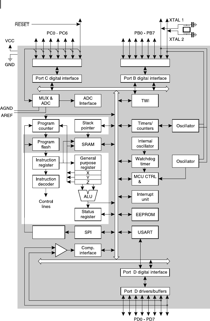
A schematic of a simpli ed internal architecture of ATmega8 is shown in Figure 14.4 . The reader is
advised to spend some time to study its salient features, some of which are already indicated.
14.4.2 AVR Core
The core of this microcontroller, labelled as AVR CPU, is the portion without any light shade within the
shaded rectangle, indicating the boundary of the controller. The core is that part of a processor, which
is responsible for fetching, decoding and executing its instructions. ATmega8 core contains a program
counter for an instruction fetch, an instruction register and instruction decoder for decoding the instruc-
tion and the ALU with other general purpose registers, status register (SREG) and the stack pointer to
execute the instruction. We shall discuss about these general purpose registers and status register, a little
later. Let us now be familiar with other functional blocks around the system bus.
14.4.3 Oscillator and Watchdog Timer
We start our discussions on architecture of ATmega8 with its internal oscillator, the block located at the
right of the SRAM block. If the reader is still unable to locate it, check the ALU and above it beyond the
general registers you should be able to locate the SRAM block. This internal RC-oscillator is capable of
generating internal system clock to run the processor. Frequency of this system clock is software program-
mable and may be selected as any one of 1.0 MHz, 2.0 MHz, 4.0 MHz and 8.0 MHz. However, ATmega8
also allows external clock source in the form of external quartz crystal with a maximum operating fre-
quency of 16 MHz to be interfaced with the pins XTAL1 and XTL2, the signal which is passed to two oscil-
lator blocks located at the right side of internal oscillator. One of these oscillator blocks is related to on-chip
timers and counters of ATmega8. The other one takes care of MCU control and timings. Note that the WDT
of the system is controlled by the internal oscillator. What is meant by WDT? A WDT generates the internal
reset at its terminal count unless it is reloaded by its count value. This service is very helpful to come out
from an in nite loop generated by some malfunctioning of the processor due to any software error.
14.4.4 Memory Blocks
The next important unit of this block diagram is the memory locations. Note that there are a total of
three of them. The rst two are designated as program ash and SRAM near the ALU area. The third
one, the EEPROM block is located at the right side of ALU, between USART and INTERRUPT UNIT
In Chapters 9 and 10, we had detailed discussions about instruction decoding, control unit and
control signal generation and the roles of PC, IR and other related registers and modules of
any processor. Being a RISC processor the core of ATmega8 is worth studying, for any person
interested in these areas. Interested readers may refer to the manufacturer’s data sheets
regarding this.
F
O
O
D
F
O
R
T
H
O
U
G
H
T
M14_GHOS1557_01_SE_C14.indd 417M14_GHOS1557_01_SE_C14.indd 417 4/29/11 5:28 PM4/29/11 5:28 PM
418 Computer Architecture and Organization
Figure 14.4 Simplified internal architecture of AVR ATmega8 microcontroller
(Courtsey : Atmel Corporation)
+
–
AVR CPU
timing
Port C drivers/buffers Port B drivers/buffers
Programming
logic
M14_GHOS1557_01_SE_C14.indd 418M14_GHOS1557_01_SE_C14.indd 418 4/29/11 5:28 PM4/29/11 5:28 PM
Embedded Systems 419
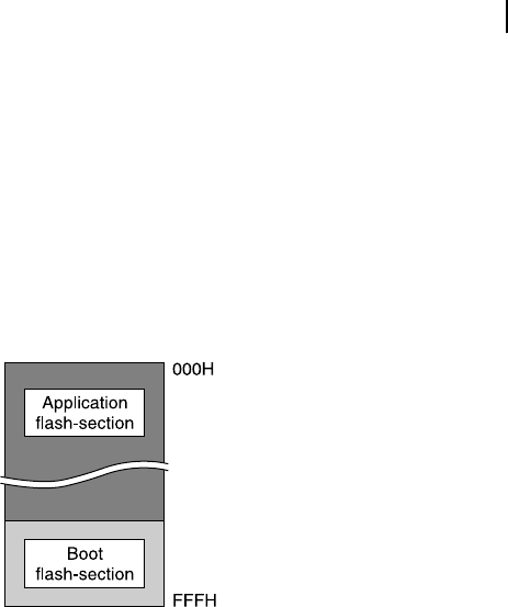
blocks. ATmega8 offers 8K bytes of program memory in the form of Flash, arranged as 4K×16-bit as all
instructions of ATmega8 are 16-bit or 32-bit wide.
For the purpose of maintaining the security of program memory, the 8K Flash is divided in two parts,
as shown in Figure 14.5. The lower part (with higher addresses) is designated as boot ash-section and
the upper part (with lower addresses) is reserved for application ash-section. The boundary between
boot-section and application-section is software programmable.
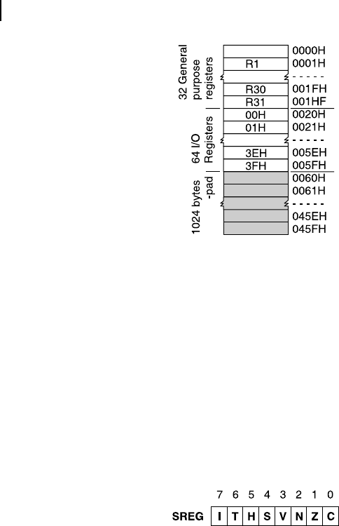
The total area of SRAM in ATmega8 is 1K bytes plus the area of general purpose registers and I/O
registers, which makes a total of 1,120 bytes, as shown in Figure 14.6. The lowest 32 address locations
within these 1,120 bytes of SRAM are reserved for 32 general purpose 8-bit registers, including three
index registers, namely X, Y and Z. We have already indicated about the register-to-register architecture,
Figure 14.5 Program memory (Flash) of ATmega8
adopted by ATmega8, allowing any of these registers to also serve the purpose of accumulator regarding
result storage.
Next 64 addresses within SRAM (refer Figure 14.6 ) are designated as I/O registers. Note that these
I/O registers have two types of addresses. One is the absolute address, as indicated in Figure 14.6
(0020H to 005FH). Their alternate addresses are from 00H to 3FH and any one of these I/O registers
may be referred through either of these two addresses. In ATmega8, each of these 8-bit I/O registers has
its own special function. For example, one of the I/O register is designated as SREG to accommodate
several ag-bits re ecting the results of some arithmetic operation. Similarly, there are I/O registers for
proper functioning of ADC, WDT, Timers and so on. The third zone of SRAM, located at the highest
address, offers 1024 bytes of scratch-pad area. These 8-bit locations may be utilized for any general
purpose data storage.
The area of EEPROM within ATmega8 is 512 bytes or 1/2 K. The reader may ask a question here
about the purpose of providing on-chip EEPROM in ATmega8. As a matter of fact, in general, some
program memory (FLASH in this case) and data memory (SRAM in this case) are generally offered by
any microcontroller for permanent and temporary data storage. Then, what is the purpose of providing
an additional storage area? To answer this question, it may be pointed out that EEPROM is the best
place to store those user-de ned data, which are permanent or semi-permanent in nature. For example,
if any system, designed around ATmega8, is to store a password of the user, it cannot be stored within
SRAM as it would not be available after switching off the system. On the other hand, FLASH is meant
for storing the program. Moreover FLASH does not permit byte-wise erasing facility, which is a must to
store the semi-permanent type of information, like a user-password. As byte-wise erasing and run-time
writing is allowed in case of EEPROM, it is an ideal choice for such type of information storage in a
exible system.
M14_GHOS1557_01_SE_C14.indd 419M14_GHOS1557_01_SE_C14.indd 419 4/29/11 5:28 PM4/29/11 5:28 PM
420 Computer Architecture and Organization
To conclude, it may be pointed out that ATmega8 does not support the provision of any external
memory either for program or for data as it is not the modern trend of embedded system design to
interface external memory with a designed system. If the 8K program memory area is found to be insuf-
cient for the system designer, then some higher version of ATmega8, e.g., ATmega16, may be used by
the designer. This is the modern trend of embedded system design.
14.4.5 Status Register (SREG)
The 8-bit status register (SREG) of ATmega8 accommodates all conditional and other ags used by the
processor, and is located at the address 005FH within I/O register area of SRAM. Bit-wise allotment of
this register is presented in Figure 14.7. There are a total of six conditional ags (C, Z, N, V, S, H), and
another two bits (T, I) are used for global interrupt control and temporary storage.
Figure 14.6 SRAM details of ATmega8
R0
Scratch
Figure 14.7 Flag-bit allotment within SREG of ATmega8
The least signi cant bit (bit 0) of SREG contains the carry ag (C) indicating any eventual carry
produced by ongoing arithmetic or logical operation. The zero ag (Z) indicates zero or non-zero result
of arithmetic or logical operation. The negative ag (N) indicates when any negative result is produced
by some arithmetic or logical operation. The V ag indicates over ow for two’s complement arithmetic
operations. The result of exclusive or (XOR) of V and N ag bits is available in S ag, the sign ag. Any
eventual half-carry generated by arithmetic operation is indicated by H ag.
Bit 6 of SREG, marked as T, serves as a temporary storage location for any bit copy operation.
Finally, the most signi cant bit of SREG, marked as I, may be used to enable or disable all interrupts
of the processor.
14.4.6 Stack Pointer and System Stack
Although ATmega8 offers 1,120 bytes of SRAM, its system stack area is restricted within the highest
1,024 bytes of SRAM. No I/O register area or general purpose register area, even unused, can accommo-
date the system stack. A 16-bit stack pointer, in the form of two 8-bit I/O registers, namely SPH and SPL,
M14_GHOS1557_01_SE_C14.indd 420M14_GHOS1557_01_SE_C14.indd 420 4/29/11 5:28 PM4/29/11 5:28 PM
..................Content has been hidden....................
You can't read the all page of ebook, please click here login for view all page.