

Project Bank 515
31. Design a small system with 8051 microcontroller and interfacing eight small LEDs with one of its
ports. Now develop a software so that the LEDs are turned on and off at random.
32. Design a small 8051 microcontroller based circuit with a small tactile switch and a small audio
speaker. Place the switch with a door or window in such a fashion so that if the door/window is
closed, the switch remains pressed and it is released when the door/window is opened. Develop the
software so that whenever the switch is not closed, the audio speaker would emit a 2 kHz square
wave signal. Try to use it as a security system of your own.
33. Assume that you have designed two systems, one with 8085 microprocessor and another with 8051
microcontroller. Now device a method by which the systems may communicate with each other and
exchange data as and when required. [HINT: 8085 offers SID and SOD signals].
P A R T – B
1. Design a 4-bit ALU with inputs A0 – A3, B0 – B3 and Cin. It is to have 4-bit output Y0 – Y3 and
Cout. The ALU would have two select lines to implement any one of the following four functions
as per the pattern of select lines.
Select lines Function Remarks
00 A + B + Cin Add with carry
01 A – B – Cin Subtract with borrow
10 A AND B Logical AND
11 A OR B Logical OR
2. Design an ALU that is capable of rotating any 4-bit number by one bit, either left or right depending
upon one function input (with two states). In case of rotating left, the most signi cant bit becomes
least signi cant bit after rotation. In case of rotating right, the least signi cant bit becomes most
signi cant bit.
3. Design an ALU capable of performing multiplication of two 4-bit numbers by producing 8-bit
result, using Booth’s algorithm. The unit may be hardware controlled in which case the complete
hardware design to be implemented. Alternately the unit may micro-coded, in which case all signals
and micro-steps are to be speci ed.
4. Design an 8051-based system capable of producing all 12 half-notes of three consecutive octaves.
The unit should have one speaker and 36 keys.
5. Design the internal architecture for a 4-bit RISC processor to be used in sales-counter billing
machines only. The billing machine would have a small 8-column numeric printer to print the bill.
It would have ten decimal keys, one decimal point key, four arithmetic function keys, one Total
key, one Print key and one Clear Last Entry key. The printer would need a 12-bit interface. Assume
all information as necessary for the design. Provision of external interrupt may be avoided and the
design should include :
R External pins and signals
R Internal registers
R ALU and necessary data paths
R Input/Output organization
R Bus for external memory interfacing.
6. Design the instruction set for the RISC processor of above problem.
Z06_GHOS1557_01_SE_C21_App_F.indd 515Z06_GHOS1557_01_SE_C21_App_F.indd 515 4/29/11 5:47 PM4/29/11 5:47 PM
516 Computer Architecture and Organization
7. Assuming that only two memory addressing modes are felt to be essential for above problem
namely Immediate and Register Indirect, ensure that necessary data paths and control signals are
provided. Present the set of micro-operations necessary to implement these two addressing modes.
Assume that the processor would offer memory mapped I/O scheme.
8. Assume that for above problem, the maximum size of external memory was allowed to be 4 kB
offering 12 address lines adopting Princeton architecture. The 12-bit Program Counter is to be gen-
erally incremented by one. For branching operation, either it is to be reloaded with an immediate
value or to be calculated by adding the offset available within a register with the present value of
the Program Counter. Design the micro-architecture necessary to implement this Program Counter
operations including all control signals and related data paths.
9. Assume that the processor would have an internal stack area of eight levels capable of storing 12-bit
return address for the same problem. Design the system stack and stack pointer with necessary data
paths and related control signals.
10. A small 8-column numeric printer has eight disc type wheels with 10 decimal digits, the decimal
point and a dash sign (-) embossed around each wheel. After completion of one-line printing opera-
tion or after reset, the printer uses the following mechanism to print the next line.
For the left-most wheel, 12 clock pulses are generated by the printer and at each clock pulse the
wheel is rotated by 30° angle. The wheel’s rotation is stopped if the printer receives a blocking signal
(from the host). The rotation and signal transmission for the next wheel starts and angular position of all
eight wheels are nalized in this manner. Then the printer’s hammer has to be activated by an external
signal from the host for printing operation. After activation of the printing-hammer, the printer auto-
matically rolls the paper one line up.
(a) Draw the timing diagram indicating the printer operation.
(b) Prepare a schematic of the hardware that are necessary for the printer, assuming a small proces-
sor is available within it.
11. A pipelined processor with two stages for instruction fetch and instruction execution is to be designed.
Instruction fetch is expected to be a completely independent operation. The instruction execution would
be completed by fetching the operands from internal registers to ALU-registers. Instruction decoding
is to be performed just after instruction fetch by placing the fetched opcode within the decoding buffer.
Assuming all instructions are of 8-bit uniform length, design the data paths and control signals for
R The instruction fetch and instruction decoding unit
R Instruction execution unit with ALU, two ALU-operand registers, one ALU result register and
eight general purpose registers.
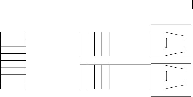
12. A super-scalar processor has a oating point unit for oating point ALU operations and an integer
unit with integer ALU for all other routine operations. The oating point unit and the integer unit
are self suf cient and independent of each other and can function simultaneously. The pre-decoding
unit selects two instructions from the instruction queue so that one is a oating point type and the
other is normal integer type and places in two separate queues for instruction decoding and execu-
tion, as shown in the schematic on following page.
Design necessary data paths and control signals for the pre-decoding unit including the instruction
queue and oating point and integer queues. Assume that if the most signi cant bit of the opcode byte
is 1, then it is a oating point instruction otherwise it is a normal integer instruction.
Z06_GHOS1557_01_SE_C21_App_F.indd 516Z06_GHOS1557_01_SE_C21_App_F.indd 516 4/29/11 5:47 PM4/29/11 5:47 PM
Project Bank 517
13. In register-to-register architecture there is no accumulator to store the result and the result from the
ALU is sent to any one of the register indicated in the instruction. Assuming that there are eight
general purpose registers, design a scheme to implement the ALU operation through the data paths
and control signals required. Note that the ALU would be provided with two additional registers to
hold the operands before and during ALU operations.
14. During its reset initialization, a processor is to clear its accumulator and program counter and load
the stack pointer by 00FFH. Design the necessary data path and control signals for this reset ini-
tialization and calculate how many clock cycles are necessary for completing the reset operation.
15. A processor offers four external vectored interrupt inputs, all of which are low level activated till it
is sensed. The processor is to take following actions if any interrupt is acknowledged
R Disable the concerned interrupt
R Save program counter value on the stack top pointed by stack pointer
R Increment the stack pointer
R Load program counter by the vector address of the active interrupt.
Assuming that four locations within the processor contains four vector addresses, design the data
path and necessary control signals for interrupt handling.
16. To return from any subroutine, a processor is to load the return address from the stack top as pointed
by the stack pointer into the program counter, decrement the stack pointer and resume its normal
execution. Design relevant data paths and all necessary control signals to implement the return
operation.
17. A processor has 16 address lines and 8 data lines and during write operation all address, data and
control signals (consider only WR signal) are active for two consecutive clock cycles to complete
the synchronous data transfer. However, if the receiving device sends the device-busy signal by
making the BUSY input of the processor high, the processor waits for integral number of two clock
cycles till BUSY goes low. After BUSY goes low the address, data and WR signal remain valid for
two more clock cycles and then the transaction is expected to be complete.
Draw the timing diagram, design all necessary control signals and design a method to implement
the data transfer operation of the processor.
18. A processor offers eight general purpose registers and another eight general purpose registers as
alternate registers. If the processor executes ALTR instruction then the presently active register set
Floating point
instruction queue
Floating point unit
Floating
point
ALU
Integer
ALU
Integer unit
Pre-decoding
unit
Instruction
queue
Integer
instruction queue
Floating point
instruction decoder
Integer
instruction decoder
Z06_GHOS1557_01_SE_C21_App_F.indd 517Z06_GHOS1557_01_SE_C21_App_F.indd 517 4/29/11 5:47 PM4/29/11 5:47 PM
518 Computer Architecture and Organization
becomes alternate registers and the alternate registers become active registers. Note that all active
registers must be connected with the ALU of the processor. Design the register set, data paths and
necessary control signals to implement register bank switching.
19. Parity is calculated from the number of 1s present in a byte or word. If this number is odd then it is
shown as odd parity by setting the parity ag (1-bit). If the number is even then it is taken as even
parity and the parity ag is cleared. Generally processors indicate the parity of the result of an ALU
operation. Assuming that the result of ALU operation is available in the result register of the ALU,
design the necessary details to indicate the parity of the result, which must be available in a 1-bit
ip- op, designated as parity ag.
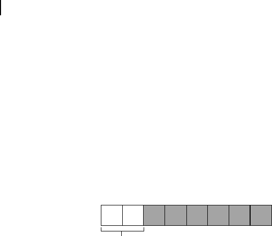
20. Opcodes of a processor is always one byte and depending upon the instruction, one, two or three
more bytes of operand might have to be fetched. This is indicated by most signi cant two bits of
the opcode ( rst byte), as illustrated below.
MSB
00 one byte
01 two bytes
10 three bytes
11 four bytes
LSB
765 432 10
Design a method of fetching necessary number of bytes for any type of instruction of the processor.
21. Swapping two nibbles of a byte is one of the instructions offered by a processor. Assuming that this
instruction is applicable only for the accumulator of the processor, design the necessary data paths
and control signals to implement it.
22. A processor offers 16 address lines and 8 data lines and its instruction set offers one instruction for
block data movement within the memory area. Before implementing this instruction, the source and
destination addresses must be loaded within registers P and Q of the processor respectively. Assume
that both P and Q are 16-bit registers. The block data movement instruction is of two bytes and the
second byte of the instruction speci es the number of bytes to be moved and to be expressed as
unsigned positive integer. Therefore, the instruction is capable of moving 0, 1 or 255 bytes from the
source to the destination area.
Design the microarchitecture of the processor to implement this instruction indicating all data paths
and control signals.
23. Arithmetic right shift is an instruction, which shifts all eight bits of the accumulator towards right
by one bit, maintaining the original sign bit (most signi cant bit). The original least signi cant bit is
driven out of the accumulator and inserted into carry ag as a temporary measure. Design the data
path and micro-control signals to implement this instruction for an 8-bit processor.
24. An 8-bit RISC processor offering 16 general purpose registers, two vectored interrupts, 16 address
lines and eight data lines to be designed around Harvard architecture. Only load and store instruc-
tions to be provided to communicate with external memory using direct and register indirect
addressing modes. The instruction set may be divided into following ve groups
R Load/Store instructions
R Arithmetic and logical instructions
Z06_GHOS1557_01_SE_C21_App_F.indd 518Z06_GHOS1557_01_SE_C21_App_F.indd 518 4/29/11 5:47 PM4/29/11 5:47 PM

Project Bank 519
R Branch and Call instructions
R Processor control instructions.
The processor is to communicate with I/O devices through memory mapped I/O scheme. Assuming
all necessary information, design the instruction format for the instruction set of the processor.
25. A processor with 20 address lines and 16 data lines is to be designed. It is to offer DMA option through
DRQ signal, which activates the DMA phase as long as it is high. The DMA request is acknowledged
by the processor through its DACK output signal, which remains high as long as DRQ remains high.
Assuming that the processor offers MRD and MWR signals for external memory read and write
operations, design the necessary microarchitecture to implement the DMA operation.
26. A processor has sixteen 8-bit general purpose registers and a 16-bit stack pointer to handle the
external stack. A PUSH register instruction places the content of the indicated 8-bit register on the
stack-top indicated by the present value of the stack pointer and the stack pointer is decremented by
one. The POP register instruction increments the stack pointer by one and the content of the stack-
top is copied into the indicated register.
Design the instruction formats for these two instructions and the necessary microarchitecture to
implement those instructions.
27. A processor is to offer power management features in form of
R Stand-by
R Idle
R Sleep
R Deep sleep modes.
The processor has an internal 8-bit register named PWRMGT, whose least signi cant two bits are used
along with the POWER mode instruction to implement the indicated power saving mode. The normal mode
of the processor is regained by the execution of system reset or an external interrupt, as illustrated below.
Design the microarchitecture to implement this power saving scheme of the processor. Note that the
clock input of the related module to be frozen to implement the power saving state for that module only.
MSB LSB
Register PWRMGT
00 Stand-by mode. Instruction fetch operation is stopped. The mode is terminated by
a reset or an external interrupt.
10 Sleep mode. Instruction fetch, ALU operations and all other dynamic features are
stopped. All external control signals (outputs) are tri-stated. This mode is terminated by
a reset and the processor starts working from the last value of the program counter.
11 Deep sleep mode. All processor operations are suspended. A system reset initializes
the processor including its program counter and its execution starts from the lowest
address of program memory.
01 Idle mode. Instruction fetch and all ALU operations are stopped. This mode is
terminated by reset or external interrupt.
765 432 10
Z06_GHOS1557_01_SE_C21_App_F.indd 519Z06_GHOS1557_01_SE_C21_App_F.indd 519 4/29/11 5:47 PM4/29/11 5:47 PM
..................Content has been hidden....................
You can't read the all page of ebook, please click here login for view all page.