

32 Computer Architecture and Organization
These tables are known as truth table and help in the representation of Boolean expressions
of various parameters. However, in truth tables, it is customary to represent off-state by 0 and
on-state by 1.
3.2.3 Boolean Identities
Identities Remarks
A.B = B.A Commutative law
A + B = B + A Commutative law
A.(B + C) = (A.B) + (A.C) Distributive law
A + (B.C) = (A + B).(A + C) Distributive law
1.A = A Identity element
0 + A = A Identity element
A.A
_
= 0 Inverse element
A + A
_
= 1 Inverse element
0.A = 0 Null law
1 + A = 1 Null law
A.A = A Idempotent law
A + A = A Idempotent law
A.(B.C) = (A.B).C Associative law
A + (B + C) = (A + B) + C Associative law
A
_
.B¯ = A
_
+ B¯ DeMorgan’s theorem
A
_
+ B¯ = A
_
.B¯ DeMorgan’s theorem
Table 3.3 Fundamental identities of Boolean algebra
In Boolean algebra, several identities are available. Using three variables, A, B and C, they are
presented in Table 3.3. The rst eight may be considered as basic rules (postulates) and others may be
derived from these basic rules. These identities may be veri ed by substituting the variables with sets of
all possible values. Note that any one variable may have either of the two values, 0 and 1.
3.3 LOGIC GATES
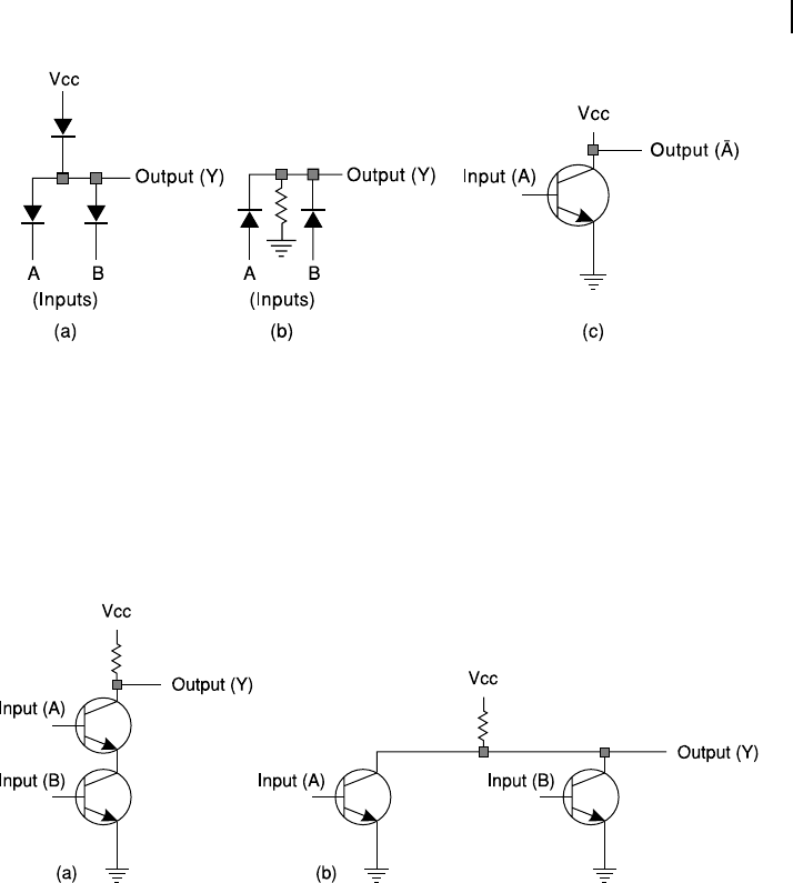
Electronically, the Boolean operators may be replaced by the combination of simple discrete devices,
e.g., diodes and transistors. Figure 3.4 cites examples of AND, OR and NOT operation by diodes and
transistor.
M03_GHOS1557_01_SE_C03.indd 32M03_GHOS1557_01_SE_C03.indd 32 4/29/11 5:01 PM4/29/11 5:01 PM
Fundamentals of Digital Logic Circuits 33
However, as per normal practice, all electronic logic gates are made from transistors [not from
diodes, as shown in Figure 3.4 (a) and (b)]. Figure 3.5 shows NAND and NOR gates constructed from
transistors. Note that after adding another transistor at the output, these two gates may be transformed
to AND and OR, respectively.
Figure 3.4 (a) AND and (b) OR operation by diodes and (c) NOT operation by transistor
Figure 3.5 (a) NAND and (b) NOR gates by transistors
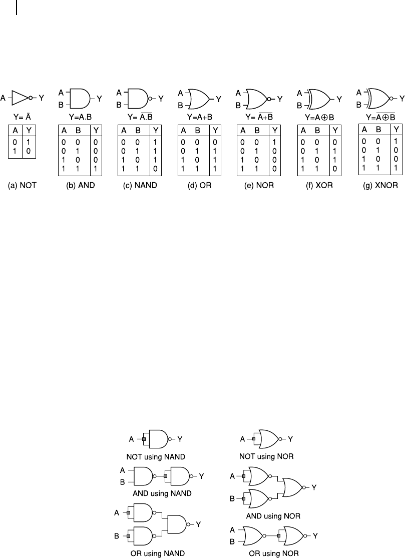
3.3.1 Common Logic Gates
Common logic gates are
R NOT R NOR
R AND R XOR and
R NAND R XNOR
R OR
Figure 3.6 presents their symbols, expressions and truth tables. Note that the inverted output of the
AND gate gives us the NAND function. Similarly, NOR is the inverted OR and XNOR is inverted XOR.
M03_GHOS1557_01_SE_C03.indd 33M03_GHOS1557_01_SE_C03.indd 33 4/29/11 5:01 PM4/29/11 5:01 PM
34 Computer Architecture and Organization
This inversion of any logic signal is represented by the bubble (small circle). Note that in the symbol of
the NOT gate, if this bubble is not present, then, the symbol denotes a buffer or a driver, which simply
boosts any digital signal without any inversion of its logic level.
Figure 3.6 Symbol and truth table for (a) NOT (b) AND (c) NAND (d) OR (e) NOR (f)
XOR and (g) XNOR gates
Logic gates shown in Figure 3.6 are having only two inputs, A and B (except the NOT gate).
However, this does not mean that logic gates cannot accept more than two inputs. As a matter of fact,
theoretically, any number of inputs is possible for all logic gates (except NOT gate, which cannot have
more than one input and XOR gate, which can not have more than two inputs). However, for all practi-
cal purposes they are manufactured with not more than eight inputs. The output in all cases would be
only one.
3.3.2 Universal Gates
Out of these seven gates, NAND and NOR gates are designated as universal gates, because of the fact
that functions of all other gates may be accomplished by various combinations of either of these two
gates. Figure 3.7 depicts how some other gates may be constructed from either NAND or NOR gates.
At the left side of Figure 3.7 , combinations from NAND gates are shown, while at the right side, NOR
gate oriented circuits are presented.
Figure 3.7 Other gates using NAND and NOR gates
M03_GHOS1557_01_SE_C03.indd 34M03_GHOS1557_01_SE_C03.indd 34 4/29/11 5:01 PM4/29/11 5:01 PM
..................Content has been hidden....................
You can't read the all page of ebook, please click here login for view all page.