
Fundamentals of Digital Logic Circuits 35
Any combination of Figure 3.7 may easily be veri ed by preparing its truth table with different
inputs. This type of circuits is known as combinational circuits as by combining different gates the
desired result is obtained. In Section 3.4, we shall discuss more about combinational circuits.
3.4 COMBINATIONAL CIRCUITS
In digital electronics, the circuits whose outputs do not change dynamically are known as combinational
circuits. In most of the cases, this dynamic change is the result of some clock input, which produces
pulses continuously, resulting a change a the output of the circuit. These dynamic circuits are designated
as sequential circuits, which we shall discuss later in this chapter.
Examples of combinational circuits are decoder , multiplexer and so on, which is discussed in this
section. In Section 3.3, we have discussed about the example of preparing an OR gate using only NAND
gates (see bottom left part of Figure 3.7 ). The representation presented in the gure can also be taken
as an example of combinational circuit. To design this circuit, we may go through the following steps
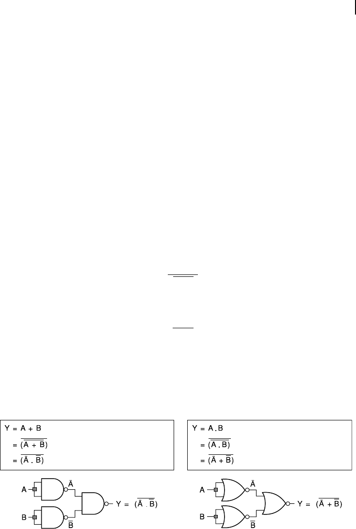
( Figure 3.8 ). For an OR gate, we may start with the following Boolean algebraic equation:
Y = A + B (3.3)
We may invert the right-hand side of the equation twice and it would still remain as a balanced equation.
Therefore, Equation (3.3) may be rewritten as
Y = (A + B) (3.4)
Now, we may apply DeMorgan’s theorem (last row of Table 3.3), and the Equation (3.4) may be
rewritten as
Y = ( A
_
.B¯) (3.5)
This indicates that after inverting both inputs, we need to use a NAND operator to generate the value
of Y. As we may use NAND operator also for inversing, this solves our problem. Replacing the AND
operator by NOR gates may also be obtained in the same way, as shown in Figure 3.8 . We now take up
two more design examples of combinational circuits, a decoder and a multiplexer.
After double inversion
OR using NAND
AND using NOR
Using DeMorgan’s theorem
After double inversion
Using DeMorgan’s theorem
Figure 3.8 Combinational circuit design using Boolean algebra
M03_GHOS1557_01_SE_C03.indd 35M03_GHOS1557_01_SE_C03.indd 35 4/29/11 5:01 PM4/29/11 5:01 PM
36 Computer Architecture and Organization
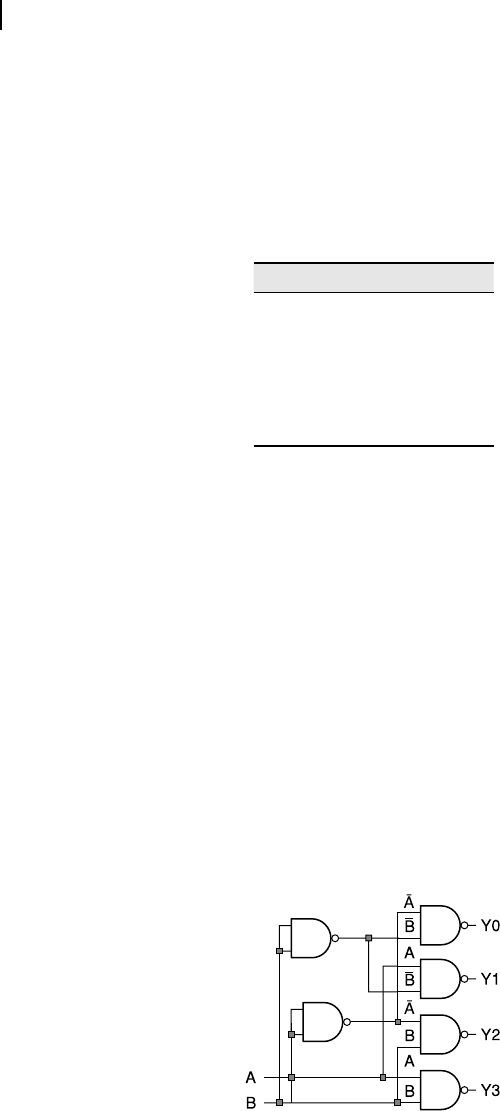
3.4.1 Decoder
Decoder is a combinational circuit, which generally has multiple ( n ) inputs and (2
n
) outputs. In
exceptional cases, it might be having only one input, in the case of 1-to-2 decoder. Out of this multiple
outputs, only one must be active for any given input pattern. As a normal practice, output signals of
decoders are active low. As an example case, let us take a 2-to-4 decoder. Truth table of a 2-to-4 decoder
is presented in Table 3.4 with A and B as input signals and Y
0
, Y
1
, Y
2
and Y
3
as output signals. Note that
A is taken as the least signi cant bit (LSB) and B is taken as the most signi cant bit (MSB).
Input Output
B A Y
0
Y
1
Y
2
Y
3
0 0 0 1 1 1
0 1 1 0 1 1
1 0 1 1 0 1
1 1 1 1 1 0
Table 3.4 Truth table of 2-to-4 decoder
From this truth table of 2-to-4 decoder, we may observe that Y
0
must be low if both A and B are low.
Using Boolean algebra, we may express this condition as
Y
0
= (A
_
.B¯) (3.6)
Similarly, cases of other three outputs may be expressed as
Y
1
= (A.B¯) (3.7)
Y
2
= (A
_
.B) (3.8)
Y
3
= (A
_
.B¯) (3.9)
Therefore, we may use four NAND gates at the output stage, and to invert signals A and B, two more
NAND gates may be incorporated. The resulting circuit is shown in Figure 3.9 . However, like any
other design case, this may not be taken as the only solution and some alternative circuits may also be
designed for implementing the function of 2-to-4 decoder.
Figure 3.9 Circuit diagram for a 2-to-4 decoder
M03_GHOS1557_01_SE_C03.indd 36M03_GHOS1557_01_SE_C03.indd 36 4/29/11 5:01 PM4/29/11 5:01 PM

Fundamentals of Digital Logic Circuits 37
3.4.2 Multiplexer
Multiplexer is a device that has multiple inputs and only one output. Generally, inputs are in the order
of 2
n
and there are n select lines. Depending upon the input pattern of these n select lines, only one input
is available as the output in an undistorted form. Schematic representation of a 4-to-1 multiplexer and
its truth table is shown in Figure 3.10 .
Decoders are widely used in microprocessor based systems to select peripheral devices. In
general, unused address lines of the processor are connected with the input of the decoder.
Each of the peripheral devices is selected by one unique output line from the decoder, which
activates the chip select input of the device when it is addressed by the processor. In Chapter 5,
we shall have an elaborate discussion on this topic.
F
O
O
D
F
O
R
T
H
O
U
G
H
T
B
4 to 1
Multiplexer
A
Input
Output
B
0
Y = P
Y = Q
Y = R
Y = S
0
1
1
(a) (b)
1
0
1
0
A
Y
P
Q
R
S
Figure 3.10 4-to-1 multiplexer (a) Schematic (b) Truth table
To pass any digital signal undistorted or to pass it as logic low, we may pass it through an AND gate,
where, some control input would allow the desired output. In this case, the control inputs have to be
derived from A and B, as per the truth table. We shall need four such AND gates, the output of which
may be connected to a 4-input OR gate. Note that at any time only one of the four AND gates would
allow the undistorted signal, while the remaining three must output logic low.
To control four AND gates, signals A and B must be used. Two inverting gates are necessary to gen-
erate proper control signals to the AND gates. The resulting circuit of 4-to-1 multiplexer is presented
in Figure 3.11 .
M03_GHOS1557_01_SE_C03.indd 37M03_GHOS1557_01_SE_C03.indd 37 4/29/11 5:01 PM4/29/11 5:01 PM
..................Content has been hidden....................
You can't read the all page of ebook, please click here login for view all page.