
40 Computer Architecture and Organization
3.6 SEQUENTIAL CIRCUITS
The electronic circuits that we have discussed so far are static in nature. In other words, their outputs do
not change with time. However, there are some digital circuits which are dynamic, i.e., their outputs are
time-dependent. These are designated as sequential circuits. Essentially, whenever we think about time,
we think about clock. This is true in digital circuits also, as all sequential circuits are clock-operated.
Therefore, to start with, we study the basic clock signal.
3.6.1 Clock Signal
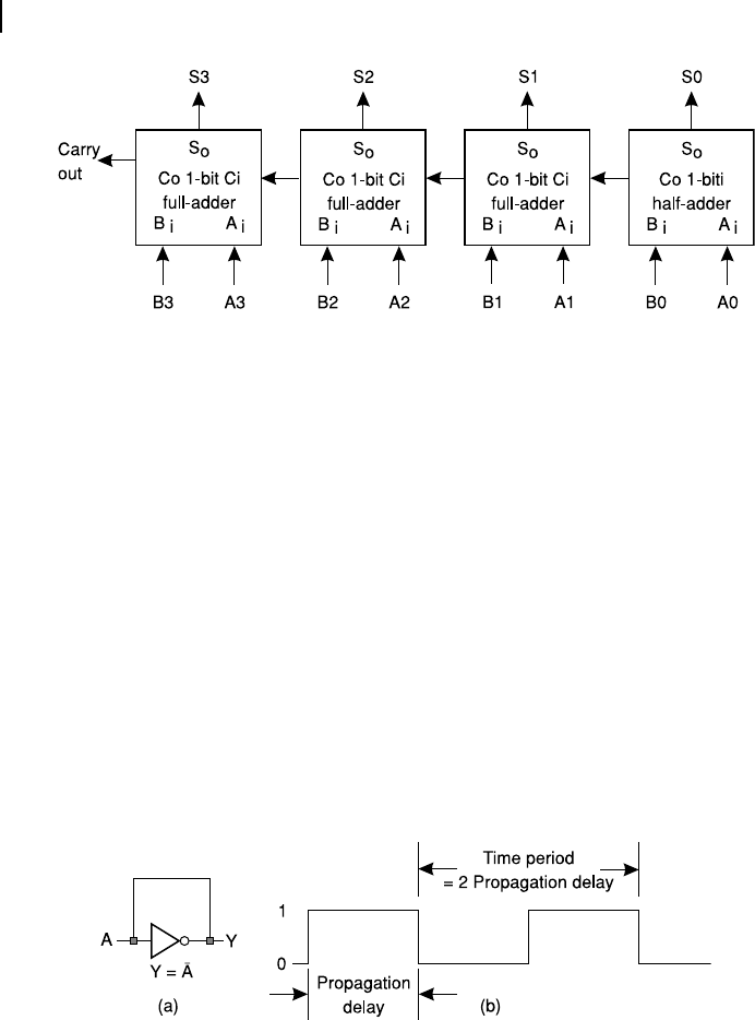
Let us assume that we have connected the output of a NOT gate with its input, as shown in Figure
3.15 (a). This type of connection is known as feedback . If we now apply power to this circuit, what
would happen? Assuming the initial input of the NOT gate to be 0 (low), then the output must be 1
(high), which would immediately become the input, because of the feedback path. Therefore, this trans-
formed input (1) would make the output 0. We may also assume the initial input as 1 instead of 0 and
arrive at the same conclusion.
Figure 3.15 (a) Basic clock from NOT gate and (b) Its waveform
As long as the circuit is active, this continuous change of output would be continued, resulting in the
waveform as shown in Figure 3.15 (b). Essentially, this is the clock waveform, which oscillates between
0 and 1 continuously. The time period of such a clock would be twice the propagation delay of the NOT
gate. What is meant by propagation delay? The time required for any change in input to be re ected at
the output stage is known as propagation delay. This depends upon various properties of the gate and
has a nite value, mentioned by the manufacturer.
Figure 3.14 Schematic of 4-bit adder using 1-bit adders
M03_GHOS1557_01_SE_C03.indd 40M03_GHOS1557_01_SE_C03.indd 40 4/29/11 5:02 PM4/29/11 5:02 PM
Fundamentals of Digital Logic Circuits 41
3.6.2 Basic Latch
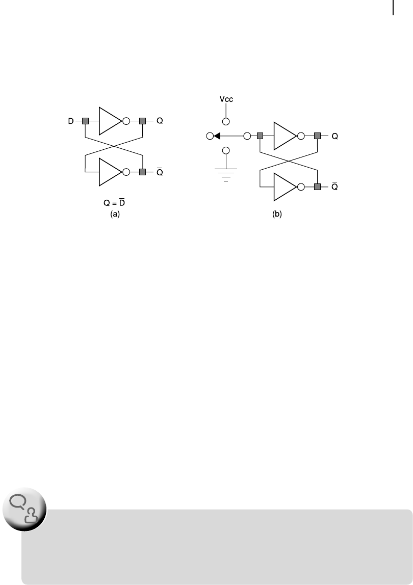
In digital circuits, a ip- op or latch is meant to retain 1-bit data. The input data may be either be 0 or 1,
therefore, a ip- op is a bi-stable device. An elementary latch may be constructed by two NOT gates, as
shown in Figure 3.16 (a).
Figure 3.16 (a) Basic latch with a pair of NOT gates (b) Data input
As shown in Figure 3.16 (a), the output Q would always be the inversion of D input. However, this
output (Q) is used as the feedback to the second (lower of the two) NOT gate, which generates an output
of Q¯ (inverted Q). This Q¯ is used as the feedback (note the double feedback, the basic characteristics of
any ip- op) for the rst NOT gate. This double feedback helps to retain the input data, even if it is not
present as input. To explain this further, let us study Figure 3.16 (b), where a 3-position switch (single
pole triple throw) is used for data entry.
Let us assume that initially the switch is connected to Vcc, producing an input of logic 1 to upper NOT
gate. Therefore, output of upper NOT gate and input of lower NOT gate would be 0. This would generate
logic 1 output from lower NOT gate, which would be input to the upper NOT gate. This condition would
remain identical (stable) even if the switch position is shifted from V
cc
to neutral (at middle of the switch).
However, if the switch is connected with the ground input (lowest position), then the input to upper
NOT gate would be 0 making Q as 1. Therefore, the input to upper NOT gate from lower NOT gate
would be 0, again maintaining the stability of the input data. This would remain so even if the switch is
shifted to its neutral (middle) position with no data input.
From the above discussions, we have learnt that
R Flip- op or latch retains any data till another fresh data input is provided.
R Flip- op or latch has two outputs that are complementary to each other.
Compare the circuits of Figure 3.16 (a) with Figure 3.15 (a). The circuit in Figure 3.15 (a) is not
a stable one and keeps on oscillating from one state to another. This oscillation is eliminated by
introducing a second NOT gate with double feedback mechanism. It may be interesting for the
reader to find out what would happen if a third NOT gate is attached with the circuit.
F
O
O
D
F
O
R
T
H
O
U
G
H
T
M03_GHOS1557_01_SE_C03.indd 41M03_GHOS1557_01_SE_C03.indd 41 4/29/11 5:02 PM4/29/11 5:02 PM

42 Computer Architecture and Organization
However, as a normal practice, ip- ops or latches are fabricated using NOR gates (or NAND gates)
with some additional circuit features. In subsequent sections, we shall discuss about the following ip-
ops, which are either basic building blocks or widely used in computer hardware
R S-R latch R J-K ip- op and
R Clocked S-R ip- op R T ip- op.
R D ip- op
3.6.3 S-R Latch
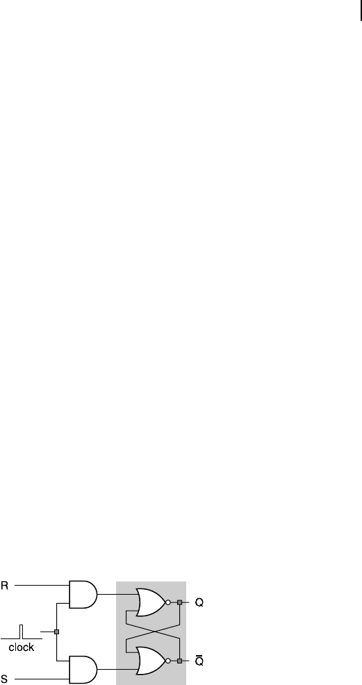
S-R latch is prepared by a pair of 2-input NOR gates inter-connected, as shown in Figure 3.17 (a). Note
the feedback connections, which are the basic characteristics of any ip- op. In this case, the gate
inputs, which do not receive any feedback, are used for logic input, designated as set (S) and reset (R).
We must remember that if R is designated as the input for a NOR gate, then Q is designated as its output.
In other words, if S is the input for one NOR gate, then Q¯ would be its output (Figure 3.17 (a)).
To start our study, initially we assume that Q is 0 (we may also assume, Q as 1, which would not
make any difference, as we shall observe shortly). We also assume that both S and R inputs are 0. In
such a condition, as S and Q, both are 0; therefore, the output from lower NOR gate (Q¯) must be 1. This
must force the output of upper NOR gate (Q) as 0, which was our original assumption, indicating that
the circuit condition is stable.
On the other hand, if we assume an initial condition of Q = 1 (with S = R = 0, as before), then the
output from lower NOR gate (Q¯) must be 0, making both inputs of the upper NOR gate as 0, resulting
in Q = 1, same as our starting assumption. Therefore, we see that the unit is capable of retaining its
original state, provided both S and R inputs are low. This is indicated in the rst of the four rows of the
characteristic table given in Figure 3.17 (c).
This R-Q or S-Q
_
relationship is the only point to be remembered in case of S-R latch. Rest of
the part is perfectly logical and may be derived any time from fundamental concepts.
F
O
O
D
F
O
R
T
H
O
U
G
H
T
Figure 3.17 (a) S-R latch (b) Timing diagram (c) Characteristic table
M03_GHOS1557_01_SE_C03.indd 42M03_GHOS1557_01_SE_C03.indd 42 4/29/11 5:02 PM4/29/11 5:02 PM
Fundamentals of Digital Logic Circuits 43
To continue our discussions on further investigations, we now assume that S input goes high (from 0
to 1), as shown in the timing diagram of Figure 3.17 (b). The other input (R) remains low. This condition
forces the output from lower NOR gate (Q¯) as 0, and for upper NOR gate, as both of its inputs are 0, its
output Q must be 1. This is again another stable state and known as setting the output as 1. What would
happen to this if S goes low at this point? We have already discussed this topic in Section 3.6.2 and we
know that Q would remain stable and would not change in such a case. Refer the second row of the table
of Figure 3.17 (c) for this correlation of input-output.
Now, we investigate the last condition, making S as low and R as high (refer the timing diagram). If
R = 1, then Q output must be low, forcing the output of the lower NOR gate (Q¯) as 1. Therefore, both
inputs of the upper NOR gate would be high, generating another stable state. The reader can now check
that when R goes low, it would leave the old state of Q unchanged. This relation is documented in the
third row of the table of Figure 3.17 (c).
At this stage, the reader may ask that what would happen to Q if both S and R inputs are high (1)?
The answer is, in that case both Q as well as Q¯ would be low, which is a stable but undesirable state
(non-complementary outputs) for any ip- op. Note that initially we have assumed that both outputs
from the ip- op would be complementary to each other. Therefore, for any S-R latch, we do not allow
both S and R inputs to be simultaneously becoming 1. Logically also, it is correct, i.e., we should not
deliver ‘ set ’ and ‘ reset ’ commands simultaneously, as these commands themselves are complementary
to each other. However, in a later section (D ip- op) we shall see that how this problem may be
eliminated.
3.6.4 Clocked S-R Flip-Flop
Figure 3.18 shows the circuit of clocked S-R ip- op. It is an upgradation of S-R latch (shaded area),
which we have discussed above. Comparing this with Figure 3.17 (a), we nd the addition of a pair of
dual-input AND gates through which S and R inputs are propagated to the NOR gate pair. A common
clock input for the pair of AND gates ensures that the S and R inputs to the NOR gates would only be
valid as long as the clock input is high. When the clock input goes low, old outputs at Q and Q¯ would
remain unchanged.
Introduction of the clock signal is essential for computer circuits as all operation of computer are
always synchronized with a central clock. However, unlike S-R latch, here the change of output would
not be instantaneous. This is known as asynchronous operation.
Figure 3.18 Clocked S-R flip-flop
M03_GHOS1557_01_SE_C03.indd 43M03_GHOS1557_01_SE_C03.indd 43 4/29/11 5:02 PM4/29/11 5:02 PM

44 Computer Architecture and Organization
3.6.5 D Flip-Flop
To eliminate the major problem of S-R ip- op (S and R inputs cannot simultaneously be high), the R
input is obtained in the D ip- op as inverted S input, because a NOT gate is placed between S and R
inputs, as shown in Figure 3.19 (a).
What is the difference between a latch and a flip-flop? As a matter of fact, both are more
or less identical in circuit. However, the general practice is to designate it as a flip-flop if the
operation is coordinated through a clock. In the absence of any such clock input, generally, we
designate it as a latch. However, in some cases this convention is not very strictly followed.
F
O
O
D
F
O
R
T
H
O
U
G
H
T
Note that in this case also, similar to clocked S-R ip- op, data would be passed to NOR gates from
D input through the AND gates only when the clock input is high (asynchronous operation). The output
would be latched at the falling edge of the clock input and would remain stable as long as D input is
not changed.
As the undistorted value of D input is available at the Q output, therefore Q¯ output is generally not
shown in the symbol of D ip- op [Figure 3.19 (b)].
3.6.6 J-K Flip-Flop
By using additional feedback signals, S-R ip- op is modi ed in another way to eliminate its inherent
dif culty of not allowing both S and R input to be 1, as shown in Figure 3.20 (a).
In this case, the output Q would remain unchanged if both J and K are 0 (Table 3.6). Resetting the
output to 0 is implemented by making K as 1. Setting the output as 1 is done by J alone, with J as 1.
Figure 3.19 D Flip-flop (a) Circuit and (b) Symbol
M03_GHOS1557_01_SE_C03.indd 44M03_GHOS1557_01_SE_C03.indd 44 4/29/11 5:02 PM4/29/11 5:02 PM
..................Content has been hidden....................
You can't read the all page of ebook, please click here login for view all page.