

48 Computer Architecture and Organization
3.9 SOLVED EXAMPLES
Example 3.1
Problem Design a circuit to implement the following Boolean function
Y = (A + B¯ ) C (3.10)
and then generate its truth table.
Solution According to the given condition, Y is the output and A, B and C are inputs. B input is to
be inverted and then logically ORed with A input. After this logical OR operation, its output has to be
logically ANDed with C input. The circuit for implementing this logic is presented in Figure 3.25 . The
truth table for this circuit is presented in Table 3.7.
Note that if C is 0, then Y must be 0. If C is 1, then Y would be 1, only if the output from the OR gate
is 1, which can happen for either A = 1 or B = 0. This is re ected in the truth table given in Table 3.7.
Note that only in three input conditions Y = 1.
ABCY
0000
0011
0100
0110
1000
1011
1100
1111
Table 3.7 Truth table for circuit of Example 3.1
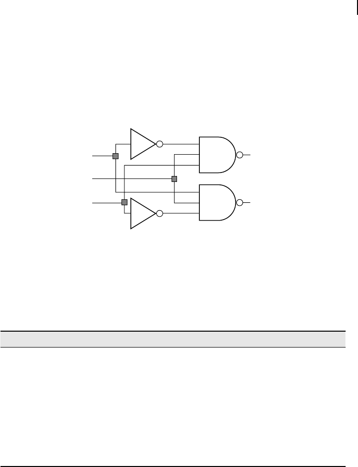
Example 3.2
Problem Design a circuit for three inputs A, B and C and two outputs Y
0
and Y
1
. Y
0
must be 0, if A =
0, B = 1 and C = 1. Y
1
must be 0, if A = 1, B = 1 and C = 0. In all other cases, both Y
0
and Y
1
must be 1.
Figure 3.25 Solution for equation of Example 3.1
M03_GHOS1557_01_SE_C03.indd 48M03_GHOS1557_01_SE_C03.indd 48 4/29/11 5:02 PM4/29/11 5:02 PM
Fundamentals of Digital Logic Circuits 49
Solution We may form two equation representing two desirable conditions for Y
0
and Y
1
. They are
Y
0
= A
_
.B.C (3.11)
Y
1
= A.B.C
¯
(3.12)
Therefore, we may use a pair of three input NAND gates and two NOT gates to prepare the circuit as
shown in Figure 3.26 .
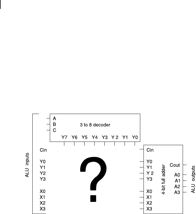
Example 3.3
Problem Design a 4-bit arithmetic-logic unit (ALU) to implement the following functions as indi-
cated in Table 3.8 according to O
0
, O
1
and O
2
inputs. Two 4-bit inputs are X (X
0
– X
3
) and Y (Y
0
– Y
3
)
and carry (Cin) is 1-bit input. Output should be 4-bit (A
0
– A
3
) along with 1-bit carry (Cout).
O
2
O
1
O
0
Function Remarks
0 0 0 X plus Y Add without carry
0 0 1 X plus Y plus Cin Add with carry
0 1 0 X minus Y Subtract without borrow
0 1 1 X minus Y minus Cin Subtract with borrow
1 0 0 X plus 1 Increment X by 1
1 0 1 X minus 1 Decrement X by 1
1 1 0 Complement of Y Complement of Y
1 1 1 Clear Clear all output bits to 0
Table 3.8 Functions of ALU of Example 3.3
Solution This is essentially a case of combinational circuit. The output must be available immedi-
ately with the availability of the input. We may start our planning with opcode decoding. Three opcode
(function select code) bits (O
0
, O
1
and O
2
) must be decoded to eight signals, each one with a speci c
task, as indicated in the table. For this purpose, we may use a 3-to-8 decoder (74138) or prepare our
combinational circuit. At the other side, we may use a 4-bit full adder, having nine inputs and ve
outputs. Now, we may plan how we should process the input signal for implementing each function
Figure 3.26 Solution circuit of Example 3.2
A
B
C
Y
0
Y
1
M03_GHOS1557_01_SE_C03.indd 49M03_GHOS1557_01_SE_C03.indd 49 4/29/11 5:02 PM4/29/11 5:02 PM
50 Computer Architecture and Organization
( Figure 3.27 ). Our idea is to pre-process the input signals in such a manner so that these pre-processed
signals, when fed to the 4-bit adder, would generate the desired output.
Add without Carry
In this case, X and Y inputs may be fed to the adder without any modi cation. However, the carry input
must be changed to 0 so that it is not considered during addition even if it is 1.
Add with Carry
No pre-processing of any data is required in this case and all input signal may be fed to the adder
directly.
Subtract without Borrow
To implement the subtraction, we may use the adder for 2’s complement addition. Therefore, the Y input
(all four bits) must be inverted and then fed to the adder. Moreover, the Cin bit of adder must receive 1,
irrespective of the external Cin condition. Therefore, the Cin input must be forced to have 1. Therefore,
two pre-processing of input signals are necessary in this case. Complement Y input (all four bits) and
change carry input to 1.
Subtract with Borrow
This would be similar to the last function and Y input would be inverted. However, as we are to consider
the carry input, we must complement it. Note that if original carry input is 0, then it becomes 1 and a
normal 2’s complement would be calculated. However, if original carry is 1 then it would be comple-
mented to 0, resulting in a calculation of 2’s complement minus 1, which is equivalent to the subtraction
of carry, when carry is 1. Therefore, in this case we complement both Y and Cin inputs before feeding
to the adder.
Figure 3.27 Partial solution of the ALU design problem
O0
O1
O2
M03_GHOS1557_01_SE_C03.indd 50M03_GHOS1557_01_SE_C03.indd 50 4/29/11 5:02 PM4/29/11 5:02 PM

Fundamentals of Digital Logic Circuits 51
Increment X by 1
To implement this function, we maintain X input as unchanged and clear all bits of Y input before feed-
ing to the adder. However, the carry input must be changed to 1, so that input value of X is incremented
by 1.
Decrement X by 1
To decrement X input by 1, we change all four bits of Y input to 1 and clear carry input. X input remains
unchanged. If these pre-processed inputs are fed to the adder, the result would be X – 1.
Complement of Y
We clear all four bits of X input as well as carry input. We also complement all four bits of Y input. After
this pre-processing, we may feed these signals to the adder to get the desired output.
All Clear
Whatever be the input signal conditions, in this case we clear all signals and then feed to the adder.
The resultant output of the adder must be all 0s. We now present in a tabular form the necessary pre-
processing of all input signals against each of the functions in Table 3.9.
Code Function
Activating
condition
Pre-
processing
For X
Pre-
processing
For Y
Pre-
processing
For Cin Remarks
000 X + Y Y
0
= 0 −− 0 Clear Cin
001 X + Y + C Y
1
= 0 −− −
010 X − YY
2
= 0 − Y
¯
1
Invert Y, set
Cin
011 X − Y − CY
3
= 0 − Y¯C
¯¯¯
in
Invert Y,
Invert Cin
100 X + 1 Y
4
= 0 − 01
Clear Y, Set
Cin
101 X − 1Y
5
= 0 − 1111 0
Make Y =
1111, clear
Cin
110 Y
¯
Y
6
= 0 0 Y¯0
Clear X,
Invert Y,
Clear Cin
111 Clear all Y
7
= 0 0 0 0
Clear X,
clear Y, clear
Cin
Table 3.9 Pre-processing table
Now, let us spend a little time to study this pre-processing table (Table 3.9). We can observe that X
input (all four bits) needs pre-processing only if the function select code is 110 (Y
6
= 0) or 111 (Y
7
=
0). Moreover, in either of these two cases X input, whatever it might be, is cleared to zero. For all other
cases, X input must remain as it is (no pre-processing required).
M03_GHOS1557_01_SE_C03.indd 51M03_GHOS1557_01_SE_C03.indd 51 4/29/11 5:02 PM4/29/11 5:02 PM

52 Computer Architecture and Organization
Y input (all four bits) needs pre-processing in six cases (no pre-processing for rst two cases).
Depending upon the requirement (Table 3.8), Y input to be either inverted (for function select code be-
ing 010, 011 or 110) or cleared (for function select code being 100 or 111) or to be changed to 1111 (for
function select code being 101).
Finally, Cin input is to be pre-processed for seven cases, making the input as 0 or inverted or set to 1.
Only in one case (function select code being 001) no pre-processing is necessary for Cin input. There-
fore, a maximum of four types of operations are necessary for the input signals
R Pass the signal as it is (or as they are)
R Clear the signal to zero
R Invert or complement the signal
R Set the signal to 1 (or 1111 depending upon the bit-width).
We shall now discuss about the mechanism of implementing all these four operations.
To implement any one of the rst two operations, we may use 2-input AND gate(s). One of the
two inputs of the AND gate may be designated as ‘switch’ [ Figure 3.28 (a)]. If the switch is 1, the
other input signal would be available at the output of the AND gate as it is ( rst operation). How-
ever, if the switch is cleared to 0, then the other input signal would also be cleared to 0 at the output
(second operation). Note that for 4-bit inputs (cases of X and Y of our problem), we would need four
numbers of 2-input AND gates, and all four switches of these four AND gates must be connected
together.
Now let us take the next two operations of inverting a signal or setting it as 1. This may be achieved
by a 2-input XOR gate with one of its input acting as the switch and the other handling the 1-bit input
signal [Figure 3.28 (b)]. If the switch is 0, then the signal would pass as it is. However, if the switch is 1,
then the signal would be inverted. The question may come that how the signal would be set to 1?
Well, in that case rst the signal must be cleared to 0 (with AND gate) and then it is to be inverted
by XOR gate.
Figure 3.28 Implementation of (a) AND switch and (b) XOR switch
M03_GHOS1557_01_SE_C03.indd 52M03_GHOS1557_01_SE_C03.indd 52 4/29/11 5:02 PM4/29/11 5:02 PM
..................Content has been hidden....................
You can't read the all page of ebook, please click here login for view all page.