

Fundamentals of Digital Logic Circuits 55
Flip- ops, registers, counters are examples of sequential circuits. Flip- op is a feedback-based cir-
cuit and has different varieties, e.g., SR, D, JK, T and so on.
POINTS TO REMEMBER
R Digital logic is amplitude based.
R NAND and NOR gates are universal gates.
R Truth tables represent the combinational circuits for all input patterns.
QUICKSAND CORNER
Data ow control and data storage are two major
building blocks of digital electronics used in com-
puters. For my students, I have always insisted to
gain hands-on experience in these areas by fabri-
cating and testing related hardware circuits in their
laboratory hours and also during term-projects.
Making these simple circuits functional, boosted
their con dence level much more than simply
reading the related materials in the form of text.
In this context, I always advised my stu-
dents to fabricate and test their hardware circuit
module-wise. This initially demands little more
time and patience, although the nal time con-
sumption becomes lesser as no last-phase debug-
ging of a yet-to-be-tested circuit is necessary.
Taking the advantage of the freedom permitted by
me, some of the groups prepared whole circuits
by interfacing all components without any step-
by-step modular testing. The result? They used to
spend three or four times more time to debug their
circuit to make it in workable condition.
REVIEW QUESTIONS
Target the Correct Option
1. Logic 0 in TTL is represented by
(a) 0 V (c) 0 V to 2.4 V
(b) 0 V to 0.8 V (d) none of these
2. Which gate is represented by following truth
table?
ABY
001
010
100
111
(a) NAND (c) XOR
(b) OR (d) none of these
3. Which of the following expression may be
taken as equivalent of the expression X.Y
(a) X¯ + Y¯ (c) X¯ –Y ¯
(b) X¯.Y¯ (d) none of these
4. Decoders are used for the purpose of
(a) ltering out unwanted data
(b) select a target device
(c) division by two
(d) none of these
5. To construct a half-adder circuit, we shall
need a XOR gate and a
(a) NOT gate (c) AND gate
(b) OR gate (d) none of these
M03_GHOS1557_01_SE_C03.indd 55M03_GHOS1557_01_SE_C03.indd 55 4/29/11 5:02 PM4/29/11 5:02 PM
56 Computer Architecture and Organization
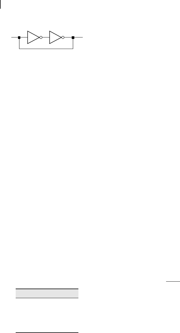
6. Which purpose is served by the following circuit?
(a) latch (c) clock
(b) driver (d) none of these
7. Which of the following ip- ops keeps on
toggling its output?
(a) S-R ip- op (c) J-K ip- op
(b) D ip- op (d) none of these
8. Which of the following devices is not associ-
ated with sequential logic?
(a) S-R latch (c) J-K ip- op
(b) multiplexer (d) none of these
9. How many function select code bits are nec-
essary to implement a 16-function ALU?
(a) 4 (c) 16
(b) 8 (d) none of these
10. In solved Example 3.3, which of the follow-
ing gates was used to clear data input signals
as and when required?
(a) NAND (c) XOR
(b) NOT (d) none of these
1. How many basic operators are there in Bool-
ean algebra? What are they?
2. What are the expressions of DeMorgan’s
theorem?
3. Which decoder has only one input?
4. What is the difference between half-adder and
a full-adder?
5. What is the limitation of a S-R latch?
6. Why D ip- op is better than clocked S-R
ip- op?
7. How can you convert an asynchronous up
counter to an asynchronous down counter?
8. How read/write memory devices are
prepared?
9. Is it possible for a 2-input XOR gate to invert
any logic signal? Justify your answer.
10. How is it possible to implement subtraction
using a full-adder?
Find in Few Seconds
Spend Some Time Here
1. Is it possible to prepare a NOT gate using
only diodes and no transistors? Justify your
answer.
2. Prepare a circuit for the following truth table.
ABY
001
011
100
110
3. Design a XOR gate using only NAND gates.
4. What would be the changes in the circuit of
Figure 3.25 if Eq. 3.10 is changed to
Y = (A + B)C
5. In solved example 3.3 it was shown how
AND gate may be used to clear any signal or
allow it to pass as it is. Similarly, XOR gate
performed inversion of signal, as and when
required. Is there any such characteristics of a
2-input OR gate? Justify your answer.
M03_GHOS1557_01_SE_C03.indd 56M03_GHOS1557_01_SE_C03.indd 56 4/29/11 5:02 PM4/29/11 5:02 PM

Fundamentals of Digital Logic Circuits 57
6. With respect to the design of solved exam-
ple 3.3, what modi cations are necessary to
change it to a 8-bit ALU?
7. Design a suitable circuit to implement the fol-
lowing function.
Y = (A + B)(B + C)(C + A)
8. How can we obtain an over ow signal when
an asynchronous 4-bit up counter over ows
from 1111 to 0000?
9. Is it possible to construct any counter using D
ip- ops? Justify your answer.
10. With only X and Y as inputs (no carry input)
design a four function 1-bit ALU for the fol-
lowing functions as per the given select code.
B A Function Remarks
0 0 X + Y Add two numbers
0 1 X – Y Subtract two numbers
1 0 X + 1 Increment X by 1
1 1 Y + 1 Increment Y by 1
Note that the output would be 1-bit (Z) along
with a carry out bit (Cout).
M03_GHOS1557_01_SE_C03.indd 57M03_GHOS1557_01_SE_C03.indd 57 4/29/11 5:02 PM4/29/11 5:02 PM
..................Content has been hidden....................
You can't read the all page of ebook, please click here login for view all page.