

Processor Basics 107
is avoided. If this automatic disabling had been avoided, then the processor would continue branching to
the same ISR repeatedly as long as the interrupting signal is active. To allow further branching for the same
interrupt, it is customary to enable the interrupt at the last stage of execution of its ISR (before executing
the RETURN instruction). Note that before execution of this enabling instruction, the ISR must ensure that
the original interrupting signal is no longer existent.
Masking also prevents the processor from reacting to any interrupt. However, in this case the pro-
cessor may have knowledge of the existence of any pending interrupting signal without any obligation
for branching to its service routine. Some processors offer a non-maskable interrupt ( NMI ), which
may never be disabled or masked. These non-maskable interrupts are necessary to react against some
extreme emergency condition, e.g., power failure (or a virus attack!). At this stage the reader must note
the difference between disabling an interrupt and masking an interrupt. In the rst case, the processor
would never know about the existence of any eventual interrupting signal, while in the second case it
can trace it. However, in either cases, no automatic branching to the ISR would be allowed.
Whatever we have discussed so far, related to processor basics, is very abstract in nature. If we study
any particular processor, we shall encounter many speci c details pertaining to that processor. In the fol-
lowing sections, we shall discuss about three processors, namely Intel 8085, Intel 8086 and Intel 8051.
Subsequently, in the advanced processor section, we shall discuss about Intel 80386 and Pentium 4.
5.7 INTEL 8085 MICROPROCESSOR
Intel 8085 was introduced around 1976 as an improvement of its preceeder, Intel 8080. This 8-bit processor
(8085) contained 6,500 transistors within a 40 pin dual in-line package (DIP ) and operated with a single
power supply of +5 volts. It worked with a maximum clock speed of 5 MHz having 8 data and 16 address
lines, capable of addressing 64 kB of memory locations (bytes) directly. Designed around Princeton archi-
tecture, 8085 does not distinguish between program and data memory. Interfaced with two more devices,
8155 and 8755, it formed a minimum working system. The IC 8755 contained 2K EPROM and two 8-bit
I/O ports. The other device, IC 8155, contained 256-bytes of RAM, three ports and a 14-bit Timer.
5.7.1 Pins and External Signals
Figure 5.12 (a) presents the pin diagram of 8085 with all of its signal nomenclature. From the designer’s
view point, the device may be taken as in Figure 5.12 (b). To make 8085 functional, minimum input
required would be Vcc, Vss, X1, X2, RESET IN, HOLD, READY and TRAP. X1 and X2 are input pins
for an external quartz crystal. Its prescribed frequency is 6.144 MHz, which is divided by 2 internally
by 8085 to generate its system clock of 3.072 MHz frequency. The RESET IN input must be low during
power on to generate a system reset. HOLD input, generally used for a DMA request, must be grounded
along with TRAP input – the non-maskable interrupt. READY input must be pulled high to make 8085
functional.
Lower 8 address signals of 8085 (A0 – A7) are multiplexed with its data bus (D0 – D7), forming the
multiplexed lower address data bus, AD0 – AD7. The falling edge of the address latch enable (ALE)
signal may be used to de-multiplex the lower address signals (A0 – A7), using an external octal latch,
e.g., 74373, if it is required by the system ( Figure 5.13 ).
5.7.2 Internal Architecture
Intel 8085 belonged to the group of earlier generation of microprocessor, when pipeline architecture
was not in vogue. Pipeline architecture was rst introduced by Intel in its rst 16-bit processor 8086,
M05_GHOS1557_01_SE_C05.indd 107M05_GHOS1557_01_SE_C05.indd 107 4/29/11 5:06 PM4/29/11 5:06 PM

108 Computer Architecture and Organization
Figure 5.13 (a) Multiplexed AD bus and ALE and (b) De-multiplexed address bus
which we shall discuss in Section 5.8. However, micro-coding was used by Intel in 8085 to reduce its
hardware overhead and, thereby, minimizing its transistor requirements.
IC 8085 was fabricated around an 8-bit ALU ( Figure 5.14 ), capable of implementing simple arithme-
tic and logical functions, without any provision of multiplication or division. Several addressing modes
were offered to help in data manipulation. The system adopted Princeton architecture, also known as
Von (pronounced as fon and NOT as bhon ) Neumann architecture, which does not distinguish between
program and data memory.
Both memory mapped I/O as well as I/O mapped I/O schemes are supported by 8085. For imple-
menting I/O mapped I/O scheme, 8085 offers the IO/M signal, which goes low during any communica-
tions with memory devices. Otherwise, this signal stays high, indicating an I/O communication.
Figure 5.14 illustrates a simpli ed internal architecture of Intel 8085. Several features of processor
architecture may be observed in this illustration. To start with, note the 8-bit internal data bus that com-
municates with various architectural modules of the processor. Next important module is the instruction
register (IR) along with the instruction decoder and machine cycle encoding module. The unidirectional
bus, inter-connecting these two modules in series, further carries the generated signals to the timing and
8085 8085
Figure 5.12 8085 (a) Pin assignments (b) Designer’s model
M05_GHOS1557_01_SE_C05.indd 108M05_GHOS1557_01_SE_C05.indd 108 4/29/11 5:06 PM4/29/11 5:06 PM

Processor Basics 109
Figure 5.14 Simplified internal architecture of Intel 8085 microprocessor
Serial I/O control
Address bus
Instruction
decoder and
machine
cycle
encoding
control module. The interrupt control and serial communication are two separate modules communicat-
ing with the remaining part of the processor through the common bus. The only module, where we can
locate the interfacing of two 8-bit bus is the address/data buffer module (shown at bottom-right corner
of the illustration), which must emit both 8-bit address (lower half) and 8-bit data during the same
machine cycle.
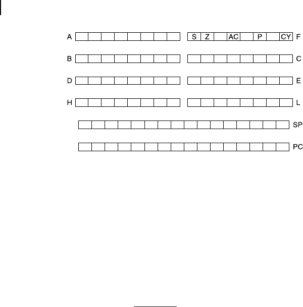
5.7.3 Register Set
Internal registers of 8085 are shown in Figure 5.15 . Out of these registers, the stack pointer (SP) and
program counter (PC) are 16-bit registers and all remaining registers are 8-bit. This includes accumula-
tor (A), ag register (F) and other six general purpose registers B, C, D, E, H and L. Note that the last
six 8-bit registers may also be used as three 16-bit registers, i.e., BC, DE and HL. When used as 16-bit
registers, they are designated by the name of the higher order of the pair. In other words, BC-pair would
be designated as B, DE-pair as D and HL-pair as H.
Five 1-bit ags are offered through the 8-bit ag register F. These ags are
R Carry (CY)
R Sign (S)
R Zero (Z)
R Parity (P)
R Auxiliary carry (AC)
Status of arithmetic and logical operations are re ected through these ags and may be used for further
decisions. Accumulator must hold one of the two operands, in these cases, and also, the result of the
operation would be available in the accumulator itself.
M05_GHOS1557_01_SE_C05.indd 109M05_GHOS1557_01_SE_C05.indd 109 4/29/11 5:06 PM4/29/11 5:06 PM
110 Computer Architecture and Organization
5.7.4 System Clock
As already indicated before, Intel 8085 needs an external crystal, and its frequency is internally divided
by two to generate the system clock. The rst machine cycle of all instructions of 8085 demand 4
T-states of this system clock. Thereafter, all subsequent machine cycles, if required by the instruction,
would need only 3 T-States. The additional T-state of the rst machine cycle of any instruction is neces-
sary to decode the instruction. All internal operations of 8085 are synchronized with this system clock.
5.7.5 System Reset
For every processor, system reset plays a vital role, as it initializes various components of the processor.
An active low reset signal through the RESET IN input pin resets 8085, which generates the following
important effects
R The PC is cleared to 0000H, which would be the address for rst instruction fetch just after
system reset.
R All interrupts (except TRAP) are disabled.
5.7.6 Instruction Set
Four major groups of instructions are offered by 8085. These groups are
R Data move
R Arithmetic operations
R Logical operations
R Program branching.
Four major addressing modes supported by 8085 are
R Immediate
R Direct
R Register direct
R Register indirect.
We shall discuss more about these issues in Chapter 6.
Figure 5.15 Internal registers of 8085 microprocessor
M05_GHOS1557_01_SE_C05.indd 110M05_GHOS1557_01_SE_C05.indd 110 4/29/11 5:06 PM4/29/11 5:06 PM

Processor Basics 111
5.7.7 Program Memory and Stack Area
With its 16 address lines, 8085 is capable of directly addressing 64 kB of memory area, which may be
in any combination of RAM and ROM, because 8085 is designed around Princeton architecture, which
we have indicated before. As 8085 starts its execution from the address 0000H, it is customary to place
program memory (ROM, PROM or EPROM) at the lowest address (or at the lower part) of the 64 kB of
directly addressable memory. This is indicated through Figure 5.16 , where 4 kB of program memory is
shown at the lowest part of 64 kB memory area as an example case.
It may be noted here that although any combination of RAM and ROM is allowed, it is customary to
place all ROM-area together and all RAM-area together. Placing RAM in-between two ROMs would
demand some jump in software part. On the other hand, placing some ROM inbetween two RAMs may
generate discontinuity in data storage operation.
System RAM may occupy any area and generally the higher address is assigned for it. For 8085, stack
may be located anywhere within the system RAM. As indicated before, the stack is always pointed by the
stack pointer (SP). In 8085, the content of SP in decremented whenever any data are placed on the stack
(PUSHed). For example, if the present value of SP is 3124H and a pair of bytes has to be saved on the sys-
tem stack, then the byte-pair would be saved in locations 3124H and 3123H and SP would be decremented
by two to make it 3122H. Note that 8085 always saves a pair of bytes on the stack-top. The content of SP
is incremented whenever any data are taken out from the stack-top (POPed). Therefore, in general, SP is
initialized at the highest available RAM address of the system, fabricated around 8085 microprocessor.
5.7.8 Interrupts
Five hardware interrupt inputs are offered by 8085, as shown in Figure 5.12 (a) and (b). It was already
indicated that out of these ve interrupts, TRAP is non-maskable and offered the highest priority. The
Figure 5.16 Memory allotment for 8085
M05_GHOS1557_01_SE_C05.indd 111M05_GHOS1557_01_SE_C05.indd 111 4/29/11 5:06 PM4/29/11 5:06 PM
..................Content has been hidden....................
You can't read the all page of ebook, please click here login for view all page.