
112 Computer Architecture and Organization
priority of an interrupt comes into consideration when two or more interrupts are generated concur-
rently. In such a situation, the interrupt with higher priority is serviced (attended) rst. TRAP is activated
by a rising edge followed by a high-level signal. RST7.5 is activated by a rising edge signal, which is
internally latched by 8085. The remaining three interrupts (RST6.5, RST5.5 and INTR) are activated
by a high-level signal, which should remain stable till the, respective, interrupt is recognized by 8085.
Priority-wise, INTR gets the lowest priority and is the only interrupt that is acknowledged by INTA out-
put of 8085. Another speciality of INTR interrupt is that the device that initializes or activates it, must supply
the branching address to 8085. Therefore, INTR is an example of non-vectored interrupt. Other four inter-
rupts of 8085 have their pre-de ned branching addresses or vector addresses as they are vectored interrupts.
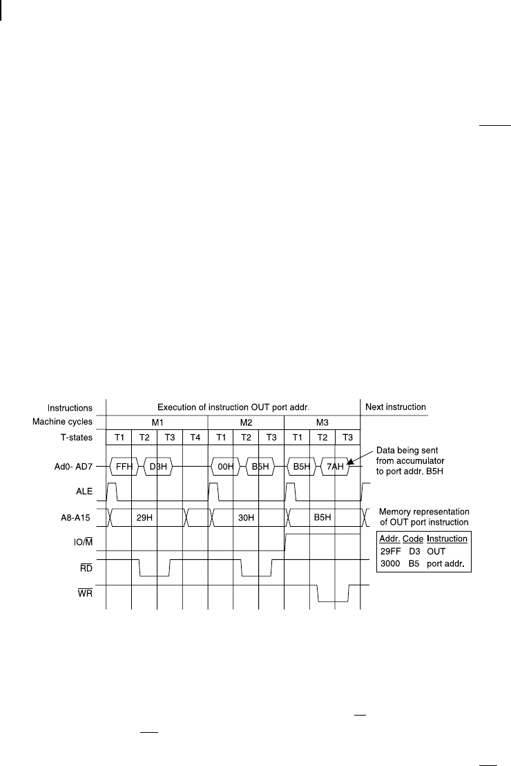
5.7.9 Timing Diagrams
Understanding any processor’s operations remains incomplete unless we study its timing diagrams. In
case of 8085, we take the instruction OUT port to study the timing details of some important signals of
8085. We have selected this instruction of 8085 because this instruction needs multiple machine cycles,
it interacts with both memory as well as I/O device and performs both read and write operations.
To start with, we assume that presently the accumulator (register A) of 8085 contains 7AH that has to
be sent (written) to the output port having the address B5H. So, the processor must use OUT instruction
whose opcode is D3H. We assume that this opcode (D3H) is available in memory location 29FFH. The
next location, 3000H must contain the port address, i.e., B5H. This information is presented within the
box at the lower right corner of Figure 5.17 .
Figure 5.17 Timing diagram for execution of ‘OUT port’ instruction of 8085
The whole operation begins with the rst machine cycle, which consumes 4 T-states. In the rst T-state
(marked as T1) a complete opcode fetch address 29FFH is sent out in two parts – AD0-AD7 and A8-A15
(Figure 5.17 ). The ALE signal also goes from high to low during T1, so that the lower address part (FFH)
may be latched by an external latch (e.g., 74373) and made available until the completion of data transaction
of this machine cycle. Note that as this is a memory related operation, IO/M output is maintained at its low.
In the second T-state (T2), RD goes low to indicate the memory device that the processor wants
to read the data, whose address is already in the address lines. It is expected that before the end of T3
data would be available in the data bus. Note that data must be valid at the rising edge of the RD signal
because it is at that particular time the processor reads the data, available in the data bus.
M05_GHOS1557_01_SE_C05.indd 112M05_GHOS1557_01_SE_C05.indd 112 4/29/11 5:06 PM4/29/11 5:06 PM
..................Content has been hidden....................
You can't read the all page of ebook, please click here login for view all page.