

Processor Basics 113
T4 of M1 is devoted for instruction decoding and thereafter, the second machine cycle starts, as the
processor already knows (after opcode decoding) that it is to bring the port address and then send the data
within accumulator to that port address. This time the processor, which has already incremented the last
emitted address within PC by one, places the address 3000H in the address bus, keeping IO/M low, as this
would be another memory read, and also lowers the RD output at T2 of this second machine cycle. The
port address B5H is sent by memory to the processor through the data bus at T3 of this machine cycle.
After getting the port address within the processor, the last machine cycle of sending the accumulator
content to that port begins by placing the port address in the address bus. Note that both the lower as
well as the upper address bus contain the same port address (B5H) as 8085 duplicates its lower address
bus to its higher address bus during I/O transaction (8085 allows only 8-bit I/O address). Being an I/O
operation, IO/M line outputs high and a write signal (WR) is activated within T2 and T3 of this last
machine cycle along with the accumulator’s data (7AH) placed on the data bus for the port (B5H). This
completes the execution of the OUT port instruction.
5.7.10 Special Features
Intel 8085 offers the direct memory access (DMA) through its HOLD input, which is acknowledged
and controlled by HLDA. The HLDA may be used to tri-state the external bus buffers as long as the
HOLD input stays high. Through SOD and SID pins, 8085 offers serial data communication feature.
The READY input may be used by slower peripheral devices to insert integral number of wait-states
during data communications. Two status indicating signals, namely S0 and S1, are provided by 8085,
which, along with IO/M signal, shows various status of the processor.
5.8 INTEL 8086 MICROPROCESSOR
Intel 8086 microprocessor was introduced in 1978 and is generally designated as a CISC processor . It
contains 29,000 transistors within a 40-pin package, operating with a single power supply of +5 volts.
It can work with a maximum clock speed of 5 MHz, having 16 data and 20 address lines, making it
capable of addressing 1 MB of memory locations (bytes) directly. An 8086 is designed around Princeton
architecture, i.e., it does not distinguish between program memory and data memory.
This microprocessor (or processor) was the rst 16-bit processor from Intel. However, it was so
well-designed that many of its features remain unchanged even in its later versions until Pentium 4 was
devised. In 8086, Intel introduced the instruction queue for the rst time to enhance its speed of execu-
tion. We shall discuss about this processor with more thoroughness, as many of the features of 8086
remain good example cases for computer architecture and organization.
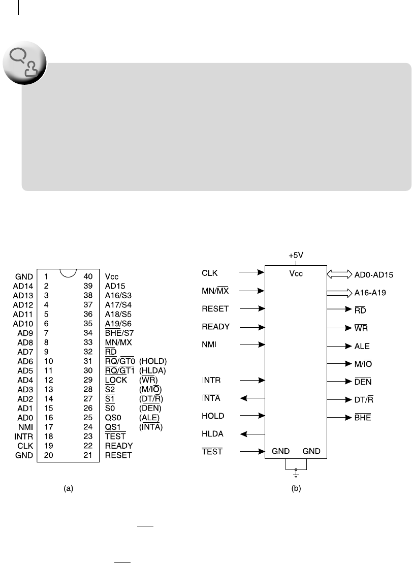
5.8.1 Pins and External Signals
Pin assignments of 8086 microprocessor are shown in Figure 5.18 (a) and the designer’s model of sig-
nals (in its minimum mode) is shown in Figure 5.18(b). Note that pin 40 is for 5 volts DC input (power
in) and two pins, pin 1 and pin 20 are for system ground connection. It has a single input for clock (pin
19) and an external device (e.g., 8284) to be used for clock generation. The reset input (pin 21) of 8086
is active high. The support device, 8284, is also capable of generating a proper reset input along with
the READY input for 8086.
It was already mentioned that 8086 has 16 data lines and 20 address lines. These 16 data lines are
multiplexed with 16 lower address lines (e.g., 8085 has done it for its 8 data lines) offering AD0 to
M05_GHOS1557_01_SE_C05.indd 113M05_GHOS1557_01_SE_C05.indd 113 4/29/11 5:06 PM4/29/11 5:06 PM
114 Computer Architecture and Organization
Figure 5.18 8086 (a) Pin assignments (b) Designer’s model
8086 8086
AD15 signals. Remaining address lines A16 to A19 are also multiplexed along with a few status signals.
The ALE signal (pin 25) may be used for de-multiplexing these lower address lines, using a pair of
external octal latch, e.g., 74373, in the same fashion as it was to be done for 8085.
A question may be asked here that why the maximum addressable memory size was not 1 M
words (double bytes)? After all, 8086 has 16 data lines and can transact 16-bit data at the
same time.
As an answer it may be pointed out that many opcodes of 8086 are of only 1-byte. Moreover,
it was designed to be interfaced with a variety of peripheral devices, some of them are 8-bit.
Therefore, if the provision was kept for transacting only 16-bit of data every time, there might
have been some unwanted complications. Therefore, this is the reason for maintaining the
minimum addressing capability within 8-bits and not 16-bits.
F
O
O
D
F
O
R
T
H
O
U
G
H
T
The next important signal is MN/MX (pin 33). If this pin receives high (logic 1) input, then 8086 would
function in its minimum mode . In that case, signals available from pins 24 to 31 would be those that are
indicated within the parenthesis of Figure 5.18 (a). In other words, pin 25 would send out the ALE signal
and pin 29 would send out the WR signal and so on. The minimum mode of 8086 indicates that there is no
other processor to share the system bus with 8086, or 8086 is the only processor to occupy the system bus.
M05_GHOS1557_01_SE_C05.indd 114M05_GHOS1557_01_SE_C05.indd 114 4/29/11 5:06 PM4/29/11 5:06 PM

Processor Basics 115
However, if MN/MX input is connected with ground (input logic 0) then 8086 would start working in
its maximum mode . In that case, pins 24 to 31 would be related with the signals that are written against
their respective pin numbers, but not within parenthesis. In this case, 8086 assumes that there is another
processor(s) to share the system bus with it, which is the case of parallel processing (Chapter 13). Note
that in such a case, control signals, e.g., ALE or WR, have to be extracted (or derived) by decoding the
status signals of 8086, i.e., S0, S1 and S2 signals externally .
Two external interrupt input pins are available in 8086. They are NMI and INTR. The rst one, NMI,
is the non-maskable interrupt (same as TRAP of 8085) and has to be used for exceptional cases, e.g.,
power failure. INTR is the general purpose interrupt input, the function of which we shall discuss in a
later section for interrupts (Section 5.8.9).
5.8.2 Internal Architecture and Registers
Figure 5.19 presents a schematic of simpli ed internal architecture of 8086 processor. As it may be
observed, the unit is divided in two parts, namely Bus Interface Unit (BIU) and Execution Unit (EU). The
BIU is exclusively devoted to handle the 20-bit address signals along with 16-bit data signals with the help
of 16-bit registers and the adder , the special function of which we shall discuss shortly. Several important
characteristics of 8086 are presented here. To start with, 8086 is equipped with a 6-byte instruction queue,
shown at the top-left corner (represented by a rectangle). During the time of decoding and executing
instruction, the processor-bus remains unoccupied. This idle time is utilized in pre-fetching a few instruc-
tion bytes from external memory and storing those within this queue. This reduces the additional time
required for fetching the next instruction, as it is readily available within the processor. This technique is
Figure 5.19 Simplified internal architecture with registers of 8086
M05_GHOS1557_01_SE_C05.indd 115M05_GHOS1557_01_SE_C05.indd 115 4/29/11 5:06 PM4/29/11 5:06 PM

116 Computer Architecture and Organization
As we can observe from Figure 5.20 , unlike the normal addition (where bit-0 of CS is added with
bit-0 of IP and so on) bit-0 of CS is added with bit-4 of IP, bit-1 of CS is added with bit-5 of IP and so on.
To start this process of shifted addition, bits 0 to 3 of IP are added with hardwired zeros. For the sake of
example, if we assume that CS and IP contain C000H and 01BFH, respectively, then after this addition,
the result would be of 20-bit, showing C01BFH. This is known as the physical address . Note that after
fetching every byte, IP is incremented by 1 by the processor itself (same way as PC is incremented by
one in 8085) and then it is added with CS in the manner as explained above.
We shall see a little later (Section 5.8.3) that this method of nal or physical address calculation
offers one major advantage. It allows the existence of multiple programs concurrently within the mem-
ory, each one earmarked with its own base address. Therefore, to switch from one program to another,
the processor has to simply save the present content of CS and IP, and reload these two registers with a
fresh set of addresses. This facility helps in multi-programming , for which 8086 was designed.
To summarize, two major duties of BIU are to pre-fetch instructions and store within the instruction
queue and to generate 20-bit address from 16-bit registers. Five 16-bit registers within BIU are desig-
nated as extra segment (ES), code segment (CS), stack segment (SS), data segment (DS) and instruction
pointer (IP). Similar to the CS register, all segment registers are expected to store the base address for
relevant operations, as indicated by their names.
The execution unit (EU) of 8086 contains the ALU, instruction decoder and other features including
a few general purpose 16-bit registers. These registers are AX, BX, CX, DX, SP, BP, SI and DI. The rst
Figure 5.20 Generation of 20-bit address in 8086
a part of pipeline architecture (discussed with more details in Chapter 12) and was introduced in 8086 to
speed up the processor’s throughput. Note that the pipeline is also a special characteristic of RISC archi-
tecture, and in 8086, we observe such effective combinations of RISC and CISC architectural specialties.
Next, we may note that there is an adder (at the top right corner of Figure 5.19 ) between memory
interface and segment registers (ES, CS and so on). What is the purpose of this adder? It may be indicated
here that all internal registers of 8086 are 16-bit as it offers a 16-bit data bus. The question may arise that
how 20-bit addresses are generated by the processor if there is no 20-bit register within it ? The answer
of it is herewith provided.
In 8086, addresses are generated in a unique way, widely different from that of 8085. Instead of one
register (PC in 8085), two registers, CS and IP are used for this purpose. One register, CS, contains the
base address. The other one, IP, contains the offset. Note that both of the registers are 16-bit registers.
The nal address is generated by adding the content of these two registers. At the time of addition of
these two 16-bit registers, a simple mechanism is used to obtain the 20-bit result. This is explained
through Figure 5.20 .
M05_GHOS1557_01_SE_C05.indd 116M05_GHOS1557_01_SE_C05.indd 116 4/29/11 5:06 PM4/29/11 5:06 PM

Processor Basics 117
four of these registers may be used as multiple 8-bit registers also. In other words, two separate and inde-
pendent 8-bit registers, AL and AH form the 16-bit register AX, and so on. AL also serves the purpose
of an 8-bit accumulator and offers some special features. SP is the stack pointer register, whose content
would be added as an offset with SS register of BIU to generate 20-bit stack address, in the same fashion
as was explained in the case of CS and IP registers.
The remaining three 16-bit registers in EU, namely base pointer (BP), source index (SI) register and
destination index (DI) register are provided to store different offset values, to be added with the DS
register (of BIU) to generate 20-bit target addresses using various addressing modes.
Intel 8086 offers a 16-bit ag register. Bit-wise ag-assignment of this register is shown in Figure 5.21 .
Lower 8-bits of this ag register matches (by functions) with the 8-bit ag register of 8085 microproces-
sor (compare with Figure 5.15 ). Thus CF, PF, AF, ZF and SF are to indicate Carry out from MSB (MSB
might be bit-7 or bit-15, depending upon the register usage), parity of result, Auxiliary carry for BCD
arithmetic, zero or non-zero result and sign of the result, respectively.
Four new (not present in 8085) ags of 8086 are trap ag (TF), interrupt ag (IF), direction ag
(DF) and over ow ag (OF). They are to be used for single stepping, interrupt handling, string direction
checking and arithmetic operations, respectively.
5.8.3 Memory Segmentation
In Sections 5.8.2, we have been already introduced to the facts that 8086 can directly address 1 MB
of memory through its 20 address lines. We have also noticed that four segment registers (ES, CS, SS
and DS) are provided to contain the base address, whereas offsets from other registers of EU are added
with these segment registers to generate the 20-bit address to communicate with external memory
devices (RAM or ROM both). It was indicated that this method offers some advantages, which we
shall discuss now.
By its designers, 8086 was allowed to execute multiple programs. It is not the exact case of paral-
lel processing. Rather it was visualized by the designers that several programs may reside within the
main memory and the processor should be able to execute a few instructions of each program (in turn)
and then switch to the next program, creating an illusion that all programs are being executed con-
currently. In computer-community the technical term adopted to express this is multi-programming .
This is because of the existence of multiple programs within the memory area, memory handling and
data security had always been the challenge for the designers of multi-programming units. In 8086, by
implementing the base-offset registers’ addition technique, the procedure of memory handling and data
security have been made easier for the programmers. Note that during the execution of any program,
the IP register (within BIU) is automatically incremented by one after fetching every byte of instruc-
tions. As the IP register is a 16-bit register, it is able to handle any 64 kB memory area. Therefore, the 1
MB memory may be segmented to smaller divisions of 64 kB each (16 such divisions are possible) and
each 64 kB segment may be allotted to one program (rather to its instruction codes). Every such seg-
ment would have a unique base address, which may be stored in a table for easier access. This feature
is illustrated through Figure 5.22 .
Figure 5.21 Details of flag register of 8086
M05_GHOS1557_01_SE_C05.indd 117M05_GHOS1557_01_SE_C05.indd 117 4/29/11 5:06 PM4/29/11 5:06 PM
..................Content has been hidden....................
You can't read the all page of ebook, please click here login for view all page.