
118 Computer Architecture and Organization
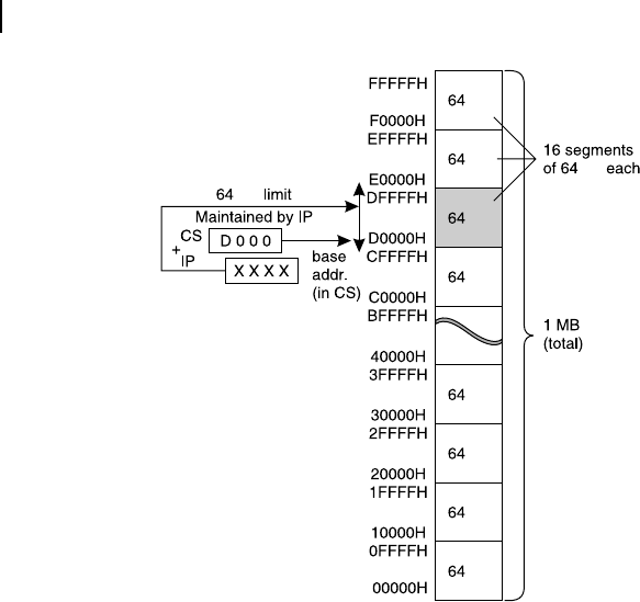
As an example, assuming a program is residing within the shaded memory block of Figure 5.22 , it
would have the base address of D000H. The physical address space available for this program would be
between D0000H and DFFFFH, which has the size of 64 kB. This 64 kB limit cannot be violated by the
16-bit offset register IP, whose value would be added with CS register to obtain the physical address.
Note that this 64 kB limit, be neither increased nor decreased. If it is decreased, then the security feature
may not be automatically implemented.
Why this scheme is unique and what trouble does it help to avoid? As an answer of the rst question,
we can ask another question is this scope of multiple program space available in 8085 ? Apparently, the
answer may be ‘why not? We may divide 64 kB of total memory available for 8085 into 16 segments of
4 kB each and place smaller programs within 4 kB limits’. The answer is partially correct. However, the
trouble would start at the time of execution of any program. The 16-bit program counter of 8085 may
cross the boundary of any 4 kB segment and trespass within the next program’s territory (may be due
to an unwanted bug in the program). There is no way of limiting the execution of the program within its
4 kB allotted block in such a situation, in the case of 8085 microprocessor.
The problem could have been solved in such a case, if 8085 offered two program counters, one
of 12-bit and the other of 4-bit. If the nal address had been generated by superimposing these two
counters, then the 4 kB segment limit could have been maintained. Therefore, 8086 offered a fool-
proof scheme of maintaining the privacy of every program or data segment by implementing the
base-offset memory addressing scheme using the segmentation technique. This is the answer for the
second question. We shall discuss more about this issue in Chapter 11 in Section 11.6 on memory
management.
kB
kB
kB
kB
kB
kB
kB
kB
kB
kB
Figure 5.22 Segmentation of 1 MB addressable memory space of 8086
M05_GHOS1557_01_SE_C05.indd 118M05_GHOS1557_01_SE_C05.indd 118 4/29/11 5:06 PM4/29/11 5:06 PM
Processor Basics 119
5.8.4 Memory Bank Addressing
In Figure 5.18 , it was shown that pin 34 of 8086 is related with bank high enable (BHE) signal. As a matter
of fact, it is related with BHE/S7 signal. However, at present we are interested only about BHE signal and
its purpose. This BHE signal is to be used for memory addressing (decoding, to be precise), along with other
20 address lines A0 – A19. Here, the question may arise that in spite of suf cient number of address signals
to address 1 MB of memory, why an extra signal would be necessary for 8086 to do so? Note that BHE has
nothing to do with I/O address decoding and, for that purpose, M/IO signal was provided (pin 28) by 8086.
To understand the reason behind providing an extra signal for memory addressing, we should rst
discuss about the major requirements for memory accessing of 8086. To start with, 8086 was planned to
be a 16-bit processor, which demands 16 data lines. If in all memory transactions only a byte (8-bits) has
to be transacted, then it would have been better to provide 8 data lines instead of 16 (in the same fashion
as it was offered in 8088 by Intel, which was used as the processor of the rst IBM PC). Therefore, for
8086, the plan was to allow the transaction of either 16-bits or 8-bits from or to system memory. We
should not forget the provision of this option.
If the provision of byte-transaction was to be provided, then every byte should be taken as a memory
location and must be targeted by address lines offered by the processor. Therefore, this is the reason for
making the maximum addressable space as 1 MB and not 1 M words (double bytes). In such a situation,
transaction of 16-bits would consume two such transactions, underutilizing 16 data lines. Therefore, the
question arises that how is it possibe to target either one or two consecutive bytes by the address lines
without generating two different patterns of addresses to do so ? This dilemma cannot be solved unless
another address-like signal is provided and that is the reason for the appearance of the BHE signal.
Let us now see how the above problem was solved in 8086.
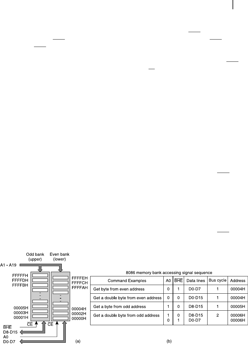
As per the plan of 8086 architects, 1 MB of memory area, addressable by 8086, was divided in two
banks, even (or lower) and odd (or higher) (refer Figure 5.23 (a) and (b) for this discussion). The even bank
contains all memory locations (RAM and ROM), whose addresses are even (ending with 0 in binary).
Similarly, the odd bank accommodates all memory locations with odd addresses (ending with 1 in binary).
Data lines D0 – D7 are connected with even bank and D8 – D15 are interfaced with odd bank. Nineteen
higher address lines (A1 – A19) of the processor are connected (after de-multiplexing) with both the mem-
ory banks. The even bank is selected by the lowest address line (A0) when A0 becomes 0, BHE is used
to select the odd bank by making it low [Figure 5.23 (a)]. These last two statements are very important .
Figure 5.23 Memory bank addressing of 8086 (a) Schematic (b) Signal sequence
FROM PROCESSOR MODULE
M05_GHOS1557_01_SE_C05.indd 119M05_GHOS1557_01_SE_C05.indd 119 4/29/11 5:07 PM4/29/11 5:07 PM

120 Computer Architecture and Organization
Therefore, to summarize, data would be transacted from even bank through D0 – D7, if A0 is low (0)
and a valid address is available through A1 – A19. Similarly, odd bank’s data transaction would take
place using D8 – D15 if BHE is low (0) and A1 – A19 provides a valid address. After this transaction, let
us see how the communication would take place.
We have already discussed that as per the requirements, data might have to be transacted either as
a byte or as a word (double byte). Intel 8086’s instruction set provides different opcodes for byte and
word transactions. As there are two banks, four different situations may occur. These four conditions are
presented in the left-most column of the Table in Figure 5.23 (b). Let us discuss all these four cases one
by one. In the following discussions, we would take up the example of reading data from the external
memory device. However, all points would be equally valid for a data write operation, too.
Let us assume that we need a byte from location 00004H. This address is in even bank. The processor
places the address 00004H (note that A0 is 0 in this case) on the address bus and BHE is kept high by
the processor. As A0 is low and BHE is high, only even bank would be selected. Within one memory
read cycle, the data byte located in memory address 00004H would be available within 8086 through
D0 – D7 lines.
The next assumption is to get a word (16-bits) starting from address 00004H. In other words, the
processor needs two consecutive bytes, one from location 00004H (belonging to even bank) and another
from 00005H (belonging to odd bank). The processor places the rst address 00004H on the address bus
(note that A0 = 0) and BHE is maintained low ( this is the trick! ). As A0 and BHE both are simultane-
ously low, at the same time both even and odd banks would be selected. Thereafter, 16-bits of data from
these two locations would move to the processor using all 16 data lines, D0 – D15 in one cycle. Note that
in this case the processor need not place the address 00005H on the address bus at any time and can still
obtain its data. The reader may verify the fact that condition of A1 – A19 and BHE are suf cient to target
the location 00005H. Condition of A0 remains irrelevant in this case. We should also note that condition
of A1 – A19 remain identical to target both 00004H and 00005H at the same time.
Our third assumption is to get one byte from the odd location 00005H, available at the odd bank. To com-
plete the task, this address, 00005H is placed on the address bus by the processor (note that A0 = 1 in this
case) and BHE is pulled down to logic low. As A0 is 1 and BHE is 0, only the odd bank would be selected.
One byte of data would then move from location 00005H to the processor using D8 – D15 data lines.
As the fourth and last case, we assume that the processor needs 16-bits of data (a word or double
byte) starting from location 00005H. In other words, the processor assumes that the lower byte is avail-
able within the address 00005H and the higher byte is available within the address 00006H. In this case,
the processor needs two cycles of memory read operation. In the rst cycle, the processor places the
lower address 00005H on the address bus (A0 = 1) and keeps BHE low to get a byte through data lines
D8 – D15. In the next cycle, the processor places the next address 00006H on the address bus (A0 = 0)
and maintains BHE as high, to get the byte from location 00006H through the data lines D0 – D7. Why
two cycles are necessary in this case? This is because, unlike our second case, condition of A1 – A19
cannot remain identical to target both 00005H as well as 00006H at the same time. The reader may
verify this fact by expanding both addresses in their binary forms.
A question may arise here (for the fourth case described) that the processor would receive a swapped
set of bytes as the lower byte is brought in through the data lines D8 – D15, while the higher byte is
brought through data lines D0 – D7. The question is correct. However, in such a situation 8086 automati-
cally places the lower byte (obtained through D8 – D15) at lower position of its internal register and the
higher byte (obtained through D0 – D7) at the higher position of the same register. The programmer is
to specify only the starting address in all four cases and the rest of the operation and control (BHE, A0
and so on) are taken care of by the processor itself.
M05_GHOS1557_01_SE_C05.indd 120M05_GHOS1557_01_SE_C05.indd 120 4/29/11 5:07 PM4/29/11 5:07 PM

Processor Basics 121
As the processor is to spend more time reading words that start from odd addresses, expert
programmers place the word (double byte) tables starting from the even address to minimize
the memory reading time.
F
O
O
D
F
O
R
T
H
O
U
G
H
T
5.8.5 System Clock
Unlike 8085, where two pins were provided with the IC to attach an external quartz crystal for generat-
ing the system clock, 8086 offers only one input, CLK (pin 19), for system clock. Therefore, an external
clock pulse generator is essential to make 8086 operational. This may be solved by interfacing the IC
8284 with 8086. The frequency of the quartz crystal attached with 8284 would be divided by three and
the proper clock pulses would be sent to 8086. For example, to make 8086 work with a frequency of
5 MHz, we have to interface a crystal of 15 MHz frequency with 8284.
This IC 8284 also helps in generating a properly synchronized reset input signal and a READY signal
for 8086. The last signal, READY, is necessary for communication of 8086 with slower peripheral devices.
5.8.6 System Reset
As discussed before, 8086 needs an active high signal at its pin 21 for a system reset. This reset signal
is generally generated through 8284, as indicated before. Reset input must remain high for at least four
clock cycles of 8086.
Whenever 8086 is reset, it clears the IP register and loads the CS register by FFFFH. This pro-
duces an effective fetch address FFFF0H. Therefore, the rst instruction to be executed by 8086 after
power-on or after reset, must be placed at this address. As the register IP is incremented by one after
every instruction byte fetch, the programmer is left with 16-bytes, starting from FFFF0H. Within these
16-bytes, a suitable unconditional jump instruction would take the program execution code fetching to
some other part of memory. Therefore, in 8086-based systems, the ROM or EPROM is placed at the
highest address of the 1 MB memory space.
This ROM is known as boot-strap ROM in computers, as it is from this ROM the booting
instructions are fetched after power-on of the system.
F
O
O
D
F
O
R
T
H
O
U
G
H
T
5.8.7 Instruction Set
Intel 8086 offers a very rich instruction set. Instructions of 8086 may be divided into the following six
major groups
R Data transfer
R Arithmetic
R Logical
M05_GHOS1557_01_SE_C05.indd 121M05_GHOS1557_01_SE_C05.indd 121 4/29/11 5:07 PM4/29/11 5:07 PM

122 Computer Architecture and Organization
R String manipulation
R Control transfer
R Processor control
Both signed as well as unsigned multiplication and division instructions are available. Special instruc-
tions are available for string manipulation. We shall discuss more about 8086 instructions in Chapter 6.
5.8.8 Stack
It is already pointed out that 8086 uses both SP as well as SS to target its stack area. In this case, SS is
taken as the base register and SP is expected to contain the offset. These two 16-bit registers are added
(as explained through Figure 5.20 ) to generate the 20-bit physical address within the earmarked stack
area. In this manner, SP can handle 64 kB of stack area.
Intel 8086 always decrements the current content of SP by 2 before placing any word (or byte) on the
stack-top (PUSH operation). Similarly, SP is incremented by 2 after any POP operation or after taking
away a word from the stack. Therefore, at the time of stack initialization, SP must be loaded with the
highest address of the stack area.
5.8.9 Interrupts
Two interrupt inputs, namely NMI (pin 17) and INTR (pin 18) are provided by 8086 for external inter-
rupt handling. INTA (pin 24) may be entrusted to acknowledge the INTR interrupt input, and not the
NMI interrupt input. Through these two interrupt input pins, 8086 provided 256 types of interrupts in
an extraordinary manner, which we shall discuss at this juncture. Note that the interrupt structure and
interrupt handling of 8086 are widely different from those of 8085.
Intel 8086 allows a total of 256 external interrupts (including NMI) and these interrupts are desig-
nated as Type 0, Type 1, Type 2 and so on, up to Type 255. At the lowest physical address of system
memory (1 MB), 8086 expects to nd an interrupt vector table of 1 kB size (from 00000H to 003FFH).
This 1 kB location is divided into 256 equal parts, allowing 4-bytes for each part. Two of these 4-bytes
are for accommodating base address and the remaining two are for holding the offset address (refer inset
of Figure 5.24 ). Either this portion should be within ROM/EPROM (non-volatile type) or in RAM. For
the last case, it is expected that, during system initialization (just after reset), this interrupt vector table
needs to be lled-up by the initializing program.
Here, we nd a major difference with 8085’s interrupt vector address scheme. For 8085, vector
addresses of four major interrupts are pre-de ned, and for INTR, the branching address has to be
supplied by the interrupting device. In 8086, all vector addresses may be planned by the system pro-
grammer and the interrupt vector table may be lled-up in such a way.
The adjective ‘top’ in the term stack-top is relative. It depends on how we represent a
memory array on a piece of paper. If we show higher address at bottom and lower addresses
on top of a memory array, then stack-top of 8086 is imaginable or the term ‘top’ is appropri-
ate. However, if lower address is shown at bottom and higher addresses at top, then we shall
need little more imagination to visualize the stack-top of 8086.
F
O
O
D
F
O
R
T
H
O
U
G
H
T
M05_GHOS1557_01_SE_C05.indd 122M05_GHOS1557_01_SE_C05.indd 122 4/29/11 5:07 PM4/29/11 5:07 PM
..................Content has been hidden....................
You can't read the all page of ebook, please click here login for view all page.