
124 Computer Architecture and Organization
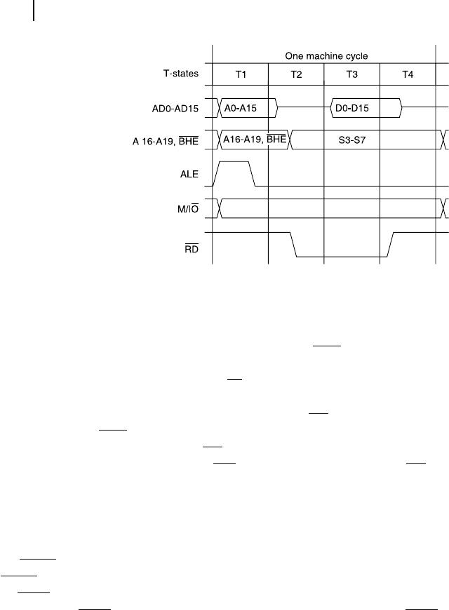
To start with, we assume a 4 T-state machine cycle for a read instruction. It is not true that all machine
cycles of 8086 are of 4 T-states. However, in many cases it is so. Note that during T1, AD0 – AD15 would
emit A0 – A15. Higher addresses A16 – A19 along with BHE would also be available during this time-
slice. The falling edge of ALE may be used to latch all these signals as they would be changing during
T2 – the next T-state. The status signal M/IO would be valid (low or high, depending upon I/O or memory
communication) from the beginning of T1 and would remain stable throughout the whole machine cycle.
As we can observe from Figure 5.25 , during T2, RD would be activated (goes low) and higher
address lines and BHE line would change to emit status signals from S3 to S7. The states T3 and T4 are
for data transactions and during T4, RD would go from low to high, indicating the end of the data read-
ing process. If it is a write cycle, then WR would act in the same way as RD signal. If wait-states are to
be inserted, it may be done between T3 and T4.
5.8.11 Special Features
Intel 8086 offers many special features, not available in 8085. For example, in its maximum mode, it outputs
the LOCK signal, which may be tested by other processors before sharing the same system bus. As long as this
LOCK output is low, it indicates that 8086 would not allow other processor(s) to gain control of the system bus.
TEST input is another feature of 8086, not available in 8085. During the execution of WAIT instruction
of 8086, if the TEST input is high, the processor would keep on waiting till TEST input goes low. After two
years of introducing 8086, Intel introduced another device in the market, which we shall discuss presently.
5.9 INTEL 8051 MICROCONTROLLER
Intel 8051 is an 8-bit microcontroller and was rst introduced in 1980. It contained 4K program mem-
ory, 128-bytes of data memory, four 8-bit I/O ports, two 16-bit timers and a USART within a 40 pin
package and operates with a single power supply of +5 volts. It can work with a normal clock speed of
12 MHz having 8 data and 16 address lines, capable of addressing 64 kB of program memory locations
(bytes) and 64 kB of external data memory locations.
Intel 8051 is one of the devices of Intel MCS-51 family of microcontrollers offering a large variety
of devices. For example, its EPROM version is designated as 8751 and ash version is designated as
Figure 5.25 Simplified timing diagram of 8086
M05_GHOS1557_01_SE_C05.indd 124M05_GHOS1557_01_SE_C05.indd 124 4/29/11 5:07 PM4/29/11 5:07 PM
Processor Basics 125
89C51. A 20-pin truncated version of this family is 89C2051 and so on. Intel 8052 or similar devices
contain 8 kB on-chip program memory, 256-bytes of data memory and an extra timer. On the other hand,
8031 is the ROM-less version of 8051. The similarity in all family members is the characteristics that
they are fabricated around the same core, i.e., all of them are capable of executing the identical instruc-
tion set. In our discussions, we take 8051 as a representative of this MCS-51 family of microcontrollers.
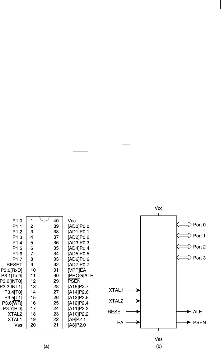
5.9.1 Pins and External Signals
External signal details of 8051 are shown in Figure 5.26 (a) and the designer’s model of signals in
Figure 5.26 (b). It may be pointed out here that microcontrollers are aimed for small-system applica-
tion and expected to function as a stand-alone device. This is the reason for incorporating program
and data memory, I/O ports and timers and the kind, in a single package. Therefore, if we compare
Figure 5.26(b) with Figure 5.12 (b) or 5.18(b), our rst observation would be that the number of sig-
nal types is less in the former case. This is because of the existence of four 8-bit I/O ports in 8051,
consuming 32 pins. These ports are bit-programmable, i.e., irrespective of the function assigned to
other port pins, any single port pin may be designated to function as either input or output. Out of
the remaining eight pins, two are necessary for power input, two for an external crystal, and one for
system reset input. This leaves three pins out of which EA is the input pin to determine the external
program memory access details and PSEN and ALE are used to access external memory.
5.9.2 Internal Architecture
While 8085 and 8086 were designed around Princeton architecture (also known as Von Neumann architec-
ture), 8051 was designed around Harvard architecture. Harvard architecture distinguishes between program
memory and data memory, while Princeton architecture does not. In other words, for processors designed
Figure 5.26 8051 (a) Pin assignments (b) Designer’s model
8051 8051
M05_GHOS1557_01_SE_C05.indd 125M05_GHOS1557_01_SE_C05.indd 125 4/29/11 5:07 PM4/29/11 5:07 PM

126 Computer Architecture and Organization
around Harvard architecture, the area earmarked for data memory cannot store any program segment. Simi-
larly, the area earmarked for program memory would not allow any data storage, not even the system stack.
If external program and data memory devices have to be interfaced with 8051, then PSEN signal has to be
used to read from external program memory and RD (alternate function of pin 17) signal has to be used
to read from external data memory. However, in majority of applications, 8051 uses its internal program
memory (4 kB) and data memory (128-bytes). Some versions of 8051 (e.g., 8052 and so on) offer 8 kB on-
chip program memory and 256-bytes of internal data memory (RAM), as we have already indicated.
Similar to 8086, 8051 also incorporated the pipeline architecture. During execution of one instruc-
tion, it pre-fetches the next byte of instruction. However, the number of bytes in its instruction queue is
only 1, which is 6 in the case of 8086.
5.9.3 Register Set
The 128-bytes of internal data memory of 8051 are divided into three functional parts, as shown in
Figure 5.27 (a). Its upper 80-bytes may be used for any general purpose usage. Lower 32-byte accom-
modates four register banks, designated as #0 to #3 [Figure 5.27 (b)]. Each of these four register banks
accommodates eight general purpose registers, as explained later in this section.
Remaining 16-bytes (from 20H to 2FH) contains 128-bits, which are directly addressable individ-
ually and designated as bit-addressable area . These bits are provided to store Boolean information,
which may be used as ags. This bit addressability feature optimizes the RAM usage, so that one full
byte is not wasted to store the information of any ag, which might have only two states of true and
false. Only one bit is suf cient in this case. The unused bytes of this bit addressable area may be used
as general purpose storage in the form of bytes, using their byte-addresses.
Each of four register banks contains eight general purpose 8-bit registers, designated as R0, R1 and
so on up to R7, as shown in Figure 5.27 (c). At any time, 8051 can use any one of the four banks and its
registers. Selection of any register bank has to be done through the special function register (SFR) des-
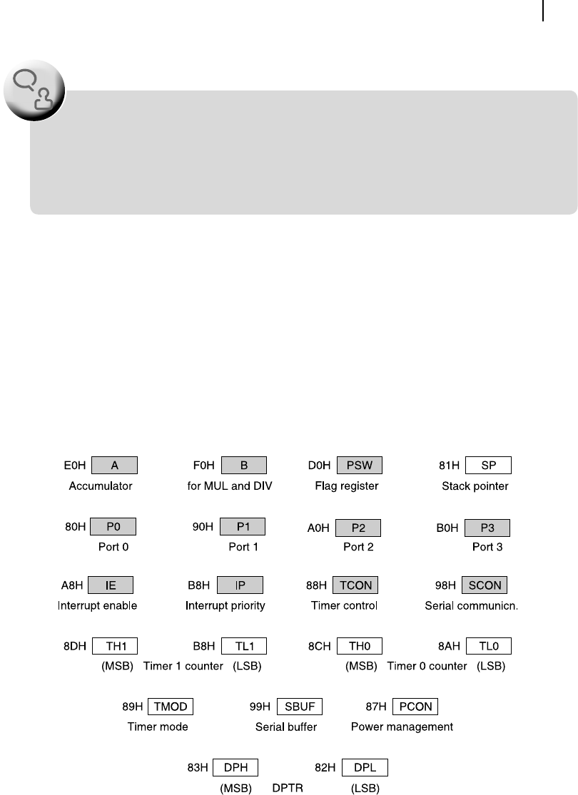
ignated as PSW. Apart from these 128-bytes of internal RAM area, which contains 32 general purpose
registers in four register banks, 8051 has 21 special function registers designated as SFRs. These 8-bit
SFRs of 8051 are shown in Figure 5.28 . Note that some of these SFRs (lightly shaded in Figure 5.28 )
are bit-addressable. Direct addresses of all SFRs are shown at their left. These SFRs are only directly
addressable, although 8051 offers indirect as well as indexed addressing modes.
Figure 5.27 (a) Internal RAM allocation details, (b) Register banks and (c) Registers
of 8051
M05_GHOS1557_01_SE_C05.indd 126M05_GHOS1557_01_SE_C05.indd 126 4/29/11 5:07 PM4/29/11 5:07 PM
Processor Basics 127
A simpler way to remember this is 8051 – 1-byte queue, while 8086 – 6-byte queue. The last
digit indicates the number of bytes of the queue. Note that queue size has nothing to do with
numbering system and this analogy is invalid for other processors. It may be assumed that
for 8051 and 8086 the correlation between their last digit of device number and length of
instruction queue is purely coincidental.
F
O
O
D
F
O
R
T
H
O
U
G
H
T
Some of important SFRs in this set are accumulator, which stores the result and B-register, which
helps (along with accumulator) in multiplication and division instructions. The ag register (PSW)
holds four ags of 8051, namely Carry (C), Parity (P), Auxiliary Carry (AC) and Overfl ow (OV).
PSW also holds two more bits, designated as RS0 and RS1 for register bank selection. Note that there is
no Z fl ag in PSW of 8051 and the concerned register is physically checked for ensuring its zero condi-
tion. The SP is an 8-bit SFR of 8051. DPTR is the only 16-bit register, which is divided into two 8-bit
registers, designated as DPH and DPL. This register, DPTR is intended to be used for accessing external
memory, program branching, and table look-up through some special instructions.
5.9.4 System Clock
Intel 8051 offers an internal clock generator, which needs only an external crystal of 12 MHz fre-
quency. Some versions of 8051 operate at higher frequencies also. One machine cycle of 8051 consumes
Figure 5.28 Special function registers (SFRs) of 8051
M05_GHOS1557_01_SE_C05.indd 127M05_GHOS1557_01_SE_C05.indd 127 4/29/11 5:07 PM4/29/11 5:07 PM
128 Computer Architecture and Organization
12 oscillations of the clock. In general, instructions of 8051 take one, two or four machine cycles to
complete their execution. Therefore, with 12 MHz crystal, one micro-second would be the execution time
taken by the shortest instructions of 8051.
5.9.5 System Reset
Intel 8051 accepts an active high reset pulse. The following actions are implemented during a system reset.
R All interrupts are disabled
R Accumulator is cleared
R PC is cleared to fetch the rst instruction from 0000H
R All ports output FFH
R SP is initialized as 07H, so that the stack starts from 08H
R PSW is cleared and, therefore, register bank #0 is selected
Note that internal 128-bytes of RAM remains unchanged after a system reset. Some SFRs of 8051 are
initialized during the system reset.
5.9.6 Instruction Set
Intel 8051 offers a wide variety of instructions, including unsigned single byte, multiply and divide
instructions. Moreover, bit-oriented instructions are also available in 8051 for loading and storing any
bit-information, logical operations and conditional branching. 8051 also offers a few nibble-oriented
instructions, useful for BCD arithmetic; and also allows relative addressing technique for all conditional
branch instructions.
5.9.7 Stack
As indicated before, 8051 offers an 8-bit SP and the internal RAM area has to be used for the system stack.
Although 8051 offers the provision of interfacing RAM and program memory externally, system stack is
not allowed in external RAM . By default, after system reset, SP is loaded by 07H and the system stack
starts from 08H. By re-initializing the value of SP, stack may be placed anywhere within the internal RAM.
Before storing any byte (PUSHing) over the stack-top, 8051 increments the SP by one. Similarly,
after taking away a byte (POPping) from the stack-top, SP is decremented by one. Therefore, SP should
be initialized at the lowest address of the system stack area.
5.9.8 Interrupts
In 8051, interrupts are allowed from
R External interrupt input pins (INT0 and INT1)
R Internal timer/counter over ow (Timer 0 and Timer 1)
R Serial data transmission or reception.
These ve interrupts have their own vector address. Note that in the case of serial communication inter-
rupt, both transmission as well as reception would have the same vector address. Also note that devices
like 8052 and the kind, offer a third timer (Timer 2), which has a separate vector address.
M05_GHOS1557_01_SE_C05.indd 128M05_GHOS1557_01_SE_C05.indd 128 4/29/11 5:07 PM4/29/11 5:07 PM
..................Content has been hidden....................
You can't read the all page of ebook, please click here login for view all page.