

The Memory System 201
of information within its ip- op, as already indicated in Chapter 3. SRAMs are mostly used for differ-
ent levels of cache memory of computers. Moreover, all the internal registers of any processor are also
composed of SRAMs.
SDRAM or Synchronous DRAM may be taken as a hybrid of previous two types, and faster than
DRAMs. Now-a–days, the main memory of many computers is being made from SDRAMs. We should
now clarify the hierarchy observed in computer memory system.
7.3 MEMORY CHARACTERISTICS AND HIERARCHY
Memory is an essential part of any computer. These are used extensively for storing various types of
program segments, data and other information. Essentially, they are expected to be read-write type of
memory. Although, as described before, that a small amount of read-only memory (ROM) is essential
for any computer system (boot strap ROM) at the time of power-on, we are not considering that aspect
in our present discussions.
As indicated before, the memory system in all computers may be categorized in two distinct labels:
R Main memory or primary memory
R Secondary memory
Although both of these are read/write type memory, secondary memories use magnetic or optical
data storage techniques while primary memory mainly depends on silicon chips. Irrespective of their
ingredients, memory system of any computer is categorized by following three parameters:
R Access time
R Cost of storage/bit
R Affordable convenient size
As all these three parameters play equally important roles in memory selection and nalization,
therefore let us spend a little time to elaborate why it is so.
7.3.1 Access Time
By the term ‘access time’ we mean the time necessary to complete a unit communication between the
processor and the concerned memory device. Essentially, access time is the time delay between issuing
In some special cases the demarcation of ROM and RAM vanishes. For example, in modern
processors, like Atmel’s AVR, a few bytes of EEPROM is provided along with FLASH and SRAM.
The purpose of this EEPROM area is to retain that information which might have to be dynami-
cally changed and yet must be retained during power-off condition. This is ideal for storing
variables like password and such kind. In this case, we find that read-only memory is being
used as a read/write memory.
F
O
O
D
F
O
R
T
H
O
U
G
H
T
M07_GHOS1557_01_SE_C07.indd 201M07_GHOS1557_01_SE_C07.indd 201 4/29/11 5:12 PM4/29/11 5:12 PM
202 Computer Architecture and Organization
the read command from the processor and the arrival of the target data within the processor. This might be
only a few nano-seconds for communication between some internal register and the processor. However, it
might be a few seconds for some magnetic tape drives. We must remember that, the more the need of access
time, the slower would be the communication and a larger time would be necessary to store or retrieve any
data. In an ideal situation, the access time should be near about zero or as minimum as possible.
7.3.2 Cost of Storage per Bit
Some storage devices are more expensive than others. For example, any magnetic tape storage would be
cheaper than any static or dynamic RAM IC. Generally, it is observed that the lower the access time, higher
is the storage cost. In other words, the access time is inversely proportional to the cost of storage per bit.
7.3.3 Affordable Convenient Size
Some memory types are capable of storing relatively larger amount of data within a suitable size. For
other type of memory, storing capability of similar amount of data may result in some impractical size.
For example, magnetic storage devices (tape drives) may be capable of storing several thousands of giga
bytes of data, within a reasonable size of spool. However, the size of any silicon wafer to store same
amount of data may not be a convenient one.
7.3.4 Memory Hierarchy
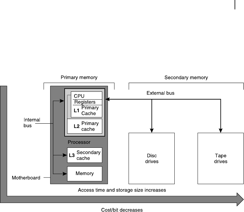
Memory hierarchy of any general computer system is presented through Figure 7.2 . We shall spend
some time with this graphical representation to elaborate few salient features depicted through it.
To start with, we shall consider six types of storage possibilities within a computer. Note that not all
six varieties of this would always be present in every computer system. These six varieties are
R Registers (closest to processor)
R L1 cache (within the same chip of the processor)
R L2 cache (or primary cache, within the same package of processor)
R L3 cache (secondary cache, outside the processor)
R Main memory (within motherboard)
R Disc drives and tape drives (outside motherboard).
The portion of memory located within mother board (of any form) is designated as primary memory
and the remaining portion (disc and tape drives) is designated as secondary memory.
Next, we should observe three boundary lines closely. The rst one, in thin line around CPU, its regis-
ters and L1 cache, represents the CPU wafer. Note that the L1 cache is a part of the CPU wafer itself, simi-
lar to CPU registers. The next boundary in thicker line represents the processor’s package, which contains
the CPU within one silicon wafer and L2 cache in another wafer. This box is designated as the processor.
The third and outermost boundary indicates the motherboard accommodating processor, L3 cache and
main memory. These boundaries indicate relative grouping of the concerned devices. For example, main
memory may be located within the same mother board, which also accommodates the processor and L3
cache. However, for the sake of clarity, we have not shown other essential parts of the motherboard.
Finally, we should note the connecting bus for all these devices or modules with the processor. The
registers and L1 cache are part of the CPU and are connected with the processor’s internal system
M07_GHOS1557_01_SE_C07.indd 202M07_GHOS1557_01_SE_C07.indd 202 4/29/11 5:12 PM4/29/11 5:12 PM
The Memory System 203
through its own internal bus (this bus is within the CPU wafer itself). L2 cache and processor are within
same package but in different wafers, connected by a special internal bus, indicated by very thin broken
line. L3 cache and main memory are connected with processor through the address-data-control bus,
which we have described in Chapter 5. This bus is shown by a thin line in Figure 7.2 . The disc drives and
tape drives are interfaced with the processor through its external bus, which is also used for interfacing
printers and other peripheral devices. This external bus is represented by a thick line.
Figure 7.2 Memory hierarchy
Registers are closest to the processor (within the processor itself) and the time necessary to com-
municate with registers would always be the minimum by any processor. However, the size and number
of these registers are small and limited, respectively, which imposes a limitation of the amount of data,
which may be stored within these registers. Cost-wise, these registers are also expensive because they
are part of the processor wafer (of silicon). Finally, it is not possible to add a few more registers with
any processor as per our own requirements. In other words, it is not exible enough.
Next comes the primary cache or L1 and L2 caches as it is generally designated. They are also the
part of the processor (either within its wafer, or a separate one within the same package of the processor).
Access time for L2 cache is little more than the access time necessary for registers, we shall explain the
reason behind it in Section 7.4 of this chapter. However, the storage area available through these caches is
much more than that of registers. Cost-wise, L1 cache is more or less identical with the internal registers
of the processor. L2 cache is less expensive than L1 cache.
Third in our storage device queue is the L3 cache or secondary cache. Note that this L3 cache is
outside the premises of the processor and is connected through the external bus. Sometimes a special
bus is offered for this L3 cache. In this case, the access time slightly increases, the available storage area
increases and the storage cost decreases with respect to the L1 and L2 caches. Note that all three types
of caches, L1, L2 and L3, are made from static RAM, which are faster to access than DRAM.
M07_GHOS1557_01_SE_C07.indd 203M07_GHOS1557_01_SE_C07.indd 203 4/29/11 5:12 PM4/29/11 5:12 PM
..................Content has been hidden....................
You can't read the all page of ebook, please click here login for view all page.