

224 Computer Architecture and Organization
Step 15 : When the number of bytes to be read becomes zero, DMA controller asks disc controller to
stop by making EOP low, which activates TC input of disc controller. The DMA controller also makes
AEN low and withdraws the HOLD request (through HRQ) by making HRQ low.
Step 16 : Once its HOLD input is low, the processor makes its HLDA output low regaining the control
of the system bus. The target le is now loaded within system RAM.
As we can understand from the above descriptions, DMA needs both hardware as well as software
coordination.
7.9 INTEL 80386 MEMORY ORGANIZATION
In Chapter 5, we have been introduced to several processors, all from Intel. These processors were 8085,
8086, 8051, 80386 and Pentium 4. The memory organization of 8085 is very straightforward with its 16
address lines and Princeton architecture. So, also is the memory organization of 8051, which is designed
around Harvard architecture. Certain special features of 8086 memory organization were highlighted in
Chapter 5 itself (Sections 5.8.3 and 5.8.4). In Section 5.11.3, we have discussed some of the essential
features of Intel 80386 processor and, in Section 5.12.2, we have discussed about Pentium 4 architecture
and cache memory. In this section and in Section 7.9.1, we shall have some more discussions about the
memory organization of 80386 and Pentium 4.
It was already indicated that 80386 was the rst Intel processor to introduce the concept of cache
memory. Although 386 did not offer any internal cache (8 kB of L1 cache was introduced in 80486,
which was released during 1989, roughly 4 years after the introduction of 80386), it allowed the neces-
sary interface for incorporating an external cache.
In Section 5.11.3, we have mentioned about virtual memory and protected mode operation of 80386.
It was indicated in Chapter 5, that in this chapter, we shall have a detailed discussion on that topic. We
pick up the thread of that discussion here and take a closer look at the protected mode operation of
80386. To start with, let us have a quick discussion on logical and physical address spaces.
7.9.1 Physical and Logical Addresses
For quicker understanding, let us put it in this way that the physical address means the memory address
(or I/O address), which is physically present within the available primary memory area (or I/O area). On
the other hand, the logical address is the address assigned by the programmer at the time of developing
the program. For example, for 8085 processor address 0000H is a physical address as it is physically
present (reset address or starting address). If this 8085 based system is equipped with a 4K program
memory, then address 0FFFH would be a physical address (last byte of the 4K EPROM). Similarly, we
DMA is an excellent example of cooperation of different devices to achive the common target.
In this case hardware and software are properly synchronized to achieve the goal, which is
efficient data transfer from one point to another.
F
O
O
D
F
O
R
T
H
O
U
G
H
T
M07_GHOS1557_01_SE_C07.indd 224M07_GHOS1557_01_SE_C07.indd 224 4/29/11 5:12 PM4/29/11 5:12 PM
The Memory System 225
may say that, for a 8086 based system, address FFFF0H must be a physical address. So, we see that all
address locations, which we can physically point out within the available memory locations (RAM or
ROM) of the processor are designated as physical memory.
The logical memory, on the other hand, is the memory addresses with which the program developer
deals with. It is the duty of the memory management unit, operating system or assembler or compiler to
change these logical addresses to physical addresses. If we use the instruction CALL DELAY, then by
the label DELAY we indicate an address of memory. At a later (or earlier) part of the same program, we
use the same label DELAY and place a small delay routine starting from that label. This way of specify-
ing memory addresses are designated as logical address. When the program is assembled, the assembler
identi es the correct address of the start of delay subroutine and that address is placed following the
opcode of CALL instruction. In 8086, the logical address is the offset address, which is added with the
base address to generate the physical address.
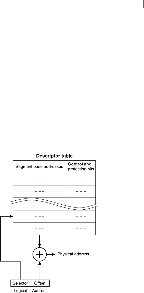
7.9.2 Selector-descriptor Tables
In case of 80386, the physical address is evaluated from logical address in a little different way with
respect to that in 8086. Intel 80386 has a memory management unit within the processor and the method
adopted by this MMU to generate the physical address from logical address is schematically presented
through Figure 7.15 . Note that the MMU of 80386 supports virtual memory and paging.
The logical address of any program written for 80386 in its real mode of operation contains two
different 16-bit parts, as it was in case of 8086. To switch between real mode and protected mode,
Figure 7.15 Schematic of simplified MMU of 80386 in real mode
M07_GHOS1557_01_SE_C07.indd 225M07_GHOS1557_01_SE_C07.indd 225 4/29/11 5:12 PM4/29/11 5:12 PM
226 Computer Architecture and Organization
the least signi cant bit of the control register CR0 within 80386 to be used. If this bit is set, 80386
enters into its protected mode of operation, while clearing this bit allows 80386 to operate in its real
mode of operation. Note that in its protected mode, the offset address is 32-bit in width. In real mode
operation, the higher and lower parts of these 16-bit addresses were designated as base address and
offset address for 8086 and by properly superimposing these two parts, 8086 generated the 20-bit
physical address. In the case of 80386 these 16-bit address parts are designated as selector address
and offset address. By the term selector address, we mean the segment selector address and this
address helps in locating the proper base address from a descriptor table , located within the MMU
(Figure 7.15 ) of 80386. The descriptor table contains base addresses of several memory locations
and a few control bits against each base address indicating privilege level and other similar informa-
tion. Once the base address is obtained from the descriptor table, the MMU adds the offset address
to generate the physical address and places within the system bus. The reader may note that this
selector-descriptor concept available in 80386 was not available in 8086.
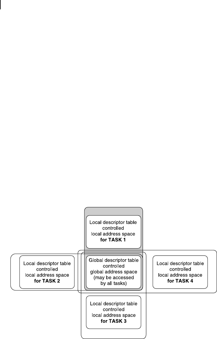
7.9.3 Protection in Multi-tasking Environment
To understand the advantage of this selector-descriptor concept, let us have a quick discussions on
multi-tasking environment allowed by 80386. As it was already explained before, multi-tasking envi-
ronment allows more than one program to be executed by the processor, paying attention only for a
small time-slice, say 25 milliseconds for each program or task.
Referring Figure 7.16 , let us assume that four different tasks are being executed by the processor.
In this case, each task would be allotted its own memory area de ned by its local descriptor table
(LDT), indicated by thicker lines in the diagram. However, the OS would be allowed the memory
area, the global address space, which would be looked after by the global descriptor table (GDT).
Figure 7.16 Data accessing for multi-tasking environment in protected mode of
80386
M07_GHOS1557_01_SE_C07.indd 226M07_GHOS1557_01_SE_C07.indd 226 4/29/11 5:12 PM4/29/11 5:12 PM
The Memory System 227
Individual tasks are allowed to share this global address space, indicated by the boundary with thin
lines in Figure 7.16. This is achieved by allowing the local tasks to access the global descriptor table
and as per the entry of this global descriptor table; only the indicated and allowed portion of the
global memory space is made accessible for a task. However, no task is allowed to use the space
allotted for other Tasks. The OS, however, is allowed the access to any part of the memory system.
Therefore, by implementing this selector-descriptor system, 80386 introduced a memory manage-
ment scheme capable of offering some amount of protection for the multi-tasking systems.
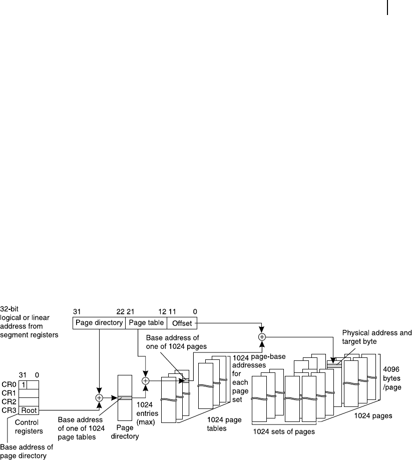
7.9.4 Paging and Page Tables of 80386
The concept of paging was explained earlier in this chapter (Section 7.7.3) and to recall it may be
indicated here that this imaginary division of main as well as secondary memory to uniform smaller
blocks help in economical memory usage. As any program in secondary memory is so divided, only the
relevant pages of that program may be loaded within the main memory for execution, and thus, saving
main memory area by not loading the complete program. Had there been no paging, then the complete
program should have been loaded within main memory to execute it. There is no xed size of a page
and it varies from system to system.
In the case of 80386, the page size is programmable, which may be as large as 4 GB. However, trans-
ferring a memory area of 4 GB from or to memory is time-consuming. Therefore, a more convenient and
smaller page size of 4 kB is adopted for quicker memory transactions. Figure 7.17 presents a schematic
of two-stage page addressing system of 80386. At a rst glance it may appear to be a bit complicated.
However, when we study it step by step, it would be easily understandable and a simple one.
Figure 7.17 The two-stage paging scheme of 80386
To start with, let us remember that 80386 switches to paging mode when the most signi cant bit of its
CR0 register is set as one (bottom left corner of Figure 7.17 ). Another control register namely CR3 holds
the root or base address of the page directory. To generate an entry point for this page directory, the root
or base address within CR3 control register is to be added with most signi cant ten bits of the logical
or linear address as it may be called, which is the 32-bit target address, the data within which is of our
present interest. As these upper 10 bits of the logical address is used for generating an entry within the
page directory, this part of the logical address is marked as Page Directory, may be observed at top left
M07_GHOS1557_01_SE_C07.indd 227M07_GHOS1557_01_SE_C07.indd 227 4/29/11 5:12 PM4/29/11 5:12 PM
..................Content has been hidden....................
You can't read the all page of ebook, please click here login for view all page.