
21
INTEGRATED CIRCUITS FOR DISPERSION COMPENSATION IN OPTICAL COMMUNICATION LINKS
21.1 MOTIVATION
Demand for highdata rates has motivated researchers to work on optical communication links in many applications. However, the most powerful computing and storage platforms we have today operate on electrical signals. The use of optical signals in a system that is predominantly electrical presents some challenges. Electrical links use copper wires and are advantageous in terms of cost but suffer from channel impairments such as skin effect and dielectric losses, especially at high frequencies. Crosstalk can be a major concern in closely spaced electrical links at high data rates. On the other hand, optical links employ optical fiber and are colloquially labeled an infinite bandwidth medium due to their low loss. Furthermore, relatively little noise is introduced along an optical fiber, and fibers can be bundled tightly together with much less crosstalk than copper wires. However, optical links mandate the use of expensive components to convert the signals between the electrical and optical domains, and their bandwidth is limited by the dispersive property of light. Dispersion occurs because the propagation delay of a light signal through an optical fiber depends on the wavelength of light and also on the light’s mode of propagation. Called dispersion, these impairments cause different portions of an optical pulse to propagate with different velocities. Consequently, closely spaced pulses carried by the optical fiber interfere with each other.
Currently, dispersion compensation in both the optical and electrical domain is a topic of active research. Although some dispersion can be easily compensated for in the optical domain, electronic dispersion compensation (EDC) is generally more cost-effective and flexible. Since dispersion can change dynamically, compensators must be adaptive. Adaptation is not easily achieved in the optical domain because of the relative lack of flexibility in optical components and because of the difficulty in extracting an appropriate error signal to control the adaptation. Moreover, silicon-integrated circuits have reached a pivotal point where they can easily provide flexible, cost-effective, low-power, and ultra-high-speed solutions that were previously impossible.
Several integrated circuit solutions to dispersion compensation in optical communication links are discussed in this chapter. In Section 21.2, different types of dispersion are briefly described. Section 21.3 introduces the use of linear filters for dispersion compensation. As examples of linear filters, finite impulse response (FIR) and infinite impulse response (IIR) filter topologies are described and measurement results are presented in Sections 21.4 and 21.5, respectively. Section 21.6 discusses nonlinear (decision feedback) dispersion compensation techniques. Alternative approaches to dispersion compensation such as maximum likelihood sequence estimation and adaptive optics are discussed in Section 21.7. Finally, Section 21.8 summarizes the findings in this chapter.
21.2 DISPERSION IN OPTICAL FIBERS
Fibers are broadly categorized into two groups. Fibers with core diameters of 50 and 62.5 µm are referred to as multimode fiber (MMF) because they can support many modes of light propagation at the optical wavelengths for which laser sources are readily available. Fibers with a core diameter of 8–10 µm support only one mode of propagation and are, hence, referred to as single-mode fiber (SMF).
The larger core size of MMF makes alignment of the fiber with another fiber or laser chip less critical. Consequently, MMF is more mechanically robust and less expensive, but suffers from more dispersion than SMF. Therefore, MMF is currently employed for links less than 1 km in length and data rates of 14 Gbit/s and lower (such as data communications within buildings via computer interconnects). On the other hand, SMF supports data rates of 40 Gbit/s over hundreds of kilometers. Currently, the rate and reach of both MMF and SMF links are limited by our ability to efficiently compensate for dispersion. The dominant forms of dispersion in commercial optical links today are chromatic dispersion and modal dispersion.
21.2.1 Chromatic Dispersion
Chromatic dispersion (CD) occurs because the refractive index of the material used to produce optical fibers has a wavelength dependence n(λ). The velocity of light in the fiber ν is related to the speed of light in free space c and the refractive index n(λ) as shown by
Any laser source modulated by random data produces spectral components spread over a range of wavelengths. Each wavelength results in a particular refractive index in the fiber and according to Eq. (21.1) propagates through the fiber at a certain speed. Consequently, different spectral components emitted by an optical source have different arrival times at the receiver, thus producing a distorted signal. Both MMF and SMF are effected by this type of dispersion.
Fortunately, chromatic dispersion compensation is not very costly and can be easily performed in the optical domain. For example, if the propagation delay of an optical fiber exhibits a known wavelength-dependency, it can be cascaded with a short section of fiber exhibiting the exact inverse wavelength-dependency. Ideally, the resulting link will be free from chromatic dispersion. Fibers can also be designed with propagation velocities that are nearly constant around the wavelength of a transmitting laser. Hence, chromatic dispersion is not the focus of most current research on integrated circuit dispersion compensation.
Modal dispersion has proven more difficult to combat.
21.2.2 Modal Dispersion
Both MMF and SMF suffer from modal dispersion. The physical mechanisms are different, but both can result in similar time-varying channel responses.
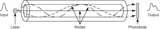
In MMF links, a single transmitted light pulse excites multiple modes of propagation along the fiber, each experiencing a different delay and attenuation. As illustrated in Figure 21.1, each optical pulse transmitted by an optical source results in multiple pulses of light at the receiver with different arrival times and amplitudes. In this manner, the transmitted optical pulse effectively “spreads out.” Note that if the optical source were transmitting only one pulse through the fiber, then pulse spreading would not be a problem. But in practice, the optical source is being modulated by random data and a train of optical pulses is being generated over the link. Due to pulse spreading, adjacent pulses interfere with each other, rendering them indistinguishable in the receiver. This phenomenon is widely known as intersymbol interference (ISI). Significant ISI results when the difference in delay between the short path (low-order modes) and the long path (high-order modes) is comparable to a bit period. To complicate matters, energy from one propagation mode can spill over into another at discontinuities along the fiber [1]. Hence, an MMF channel response can change dramatically when a fiber or connector is mechanically stressed. A practical trick that mitigates dispersion in MMF is to introduce an intentional offset between the light source and the center of the main fiber by using a short section of fiber called a “patch cord.” Doing so excites fewer modes of propagation and can therefore reduce the spread in propagation delay.
Figure 21.1. Pulse spreading due to modal dispersion in MMF. A light pulse launched at the input of the fiber takes different paths (modes) to the photodetector, resulting in different arrival times at the receiver. This causes intersymbol interference (ISI) at the receiver.
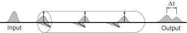
In SMF, although only a single mode of light propagation is supported, dispersion still arises due to asymmetries in the fiber cross section. The asymmetries may be due to imperfections during manufacture, or due to mechanical stress after manufacture. Each pulse of light has energy in two orthogonal modes of polarization, which, due to the asymmetries, propagate with different velocities and attenuation. As a result, again, single optical pulses may split into two pulses by the time they reach the receiver. This phenomenon is referred to as polarization mode dispersion (PMD).
PMD is a result of birefringence, which affects all real optical fibers. Birefringence refers to the difference in refractive index experienced by light in the two orthogonal polarization modes of the fiber. It is caused by ellipticity of the fiber cross section due to asymmetric stresses applied to the fiber during or after manufacturing. Birefringence leads to fast and slow modes of propagation and consequently dispersion [2].
In terms of digital communications, PMD results (to a first order) in an input pulse being split into a fast and slow pulse that arrive at the receiver at different times, as shown in Figure 21.2. If the differential delay of the two pulses is significant compared to the bit period, ISI and an increase in bit error rate (BER) will result.
Figure 21.2. Pulse bifurcation due to PMD. The power in the input pulse is split between the two polarization modes of the fiber. Birefringence causes a difference in phase velocities between the two modes, resulting in ISI at the output.
To a first order, the impulse response of an optical fiber with PMD is [3]
(21.2)
![]()
where γ is the proportion of the optical power in the “fast” state of polarization (SOP), (1 − γ) is the proportion of power in the “slow” SOP, and Δτ is the differential group delay (DGD) between the fast and slow components.
Both γ and Δτ vary, depending on the particular fiber and its associated stresses. The value of γ can be anywhere from zero to one, with uniform probability throughout this range [4] whereas Δτ varies statistically according to a Maxwellian distribution [5], given by
(21.3)
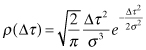
The distribution is defined by σ, which is related to the average DGD, Δτavg, by [6]
(21.4)
![]()
Therefore, though it can vary to large values, Δτ will for the most part remain close to some average value. Furthermore, Δτ varies with time, and significant variations can be observed on the order of milliseconds [7].
The average DGD per unit length of a fiber is
defined as its PMD parameter, which has units of ![]() . Typical installed fibers exhibit a PMD of
. Typical installed fibers exhibit a PMD of ![]() [8]. New fibers can be manufactured
with a PMD of as low as
[8]. New fibers can be manufactured
with a PMD of as low as ![]() [9]. Given
the PMD parameter, the average DGD of a fiber of length L is given by
[9]. Given
the PMD parameter, the average DGD of a fiber of length L is given by
(21.5)
![]()
It has been calculated that to prevent PMD from causing system outages amounting to more than 30 s per year (corresponding to an outage probability of 10−6), the average DGD must be less than approximately 15% of a bit period, TB [10]:
(21.6)
![]()
This has severe
implications as the data rate of these systems is increased to 10 and 40 Gbit/s. As
the data rate is increased on a given fiber, the maximum useful length of the fiber
decreases according to the square of the increase. For example, given a fiber with a
PMD of ![]() and using (21.6), the maximum
length of a 2.5-, 10-, and 40-Gbit/s system is 3600, 225, and 14 km, respectively,
if PMD is the limiting factor.
and using (21.6), the maximum
length of a 2.5-, 10-, and 40-Gbit/s system is 3600, 225, and 14 km, respectively,
if PMD is the limiting factor.
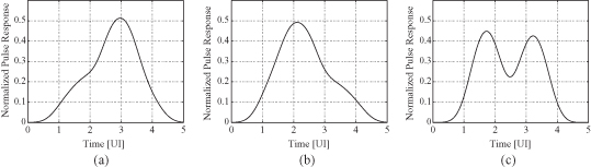
Dispersion due to multimode propagation in MMF and polarization mode dispersion in SMF are referred to, together, as modal dispersion. Figure 21.3 illustrates three possible effects of modal dispersion on the pulse response of a 10-Gbit/s link over 220 m of MMF with a patch cord. In all three cases, the pulse response is confined to roughly 3 baud unit intervals (UI) or 300 ps at 10 Gbit/s. In Figure 21.3a, a fast mode of propagation is visible preceding the main pulse causing each bit to interfere with two preceding bits. This is called a precursor response because it has mostly precursor intersymbol interference (ISI).The pulse response in Figure 21.3b, on the other hand, has a slow mode of propagation following the main pulse resulting in mostly postcursor ISI. In Figure 21.3c, the channel response has two distinct pulses that are nearly equal in amplitude and clearly separated in time. Any receiver for this channel will face some ambiguity in determining which pulse is the “main” one. We shall see that the resulting confusion necessitates nonlinear receiver architectures.
Figure 21.3. Example fiber channel pulse responses. (a) Precursor ISI pulse. (b) Postcursor ISI pulse. (c) Split pulse response.
(Copyright IEEE 2008.)
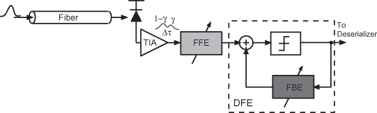
The normalized frequency responses corresponding to the three test cases in Figure 21.3 have a bandwidth of approximately 2 GHz as shown in Figure 21.4. This is well below the bandwidth required for a 10-Gbit/s optical system. Furthermore, modal dispersion can vary significantly within a few milliseconds [7], demanding an adaptive approach to EDC. A receiver architecture that performs EDC and can be easily configured to adapt to variations in modal dispersion is shown in Figure 21.5. It comprises a transimpedance amplifier (TIA), a feedforward equalizer (FFE), and a decision feedback equalizer (DFE). After necessary amplification by the TIA, the FFE mitigates ISI by linearly filtering the received signal, inverting the channel response. Such linear equalization of the channel is considered in Section 21.3–21.5. However, the split pulse response in Figure 21.4c proves to be more problematic. Since the frequency response has deep nulls, a portion of the transmitted spectrum is essentially lost and cannot be recovered by linearly filtering the received signal. For these cases, nonlinear methods for recovering the data using a DFE are discussed in Section 21.6.
Figure 21.4. Example fiber channel frequency responses. (a) Precursor ISI pulse. (b) Postcursor ISI pulse. (c) Split pulse response.
(Copyright IEEE 2008.)
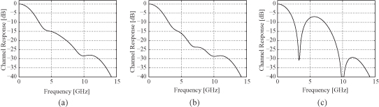
Figure 21.5. Electronic dispersion compensation (EDC) by using linear and nonlinear filters in a fiber-optic receiver.
21.3 ELECTRONIC DISPERSION COMPENSATION (EDC) USING LINEAR EQUALIZATION
A straightforward and potentially low-power method for mitigating ISI is to employ an adaptive linear filter that equalizes the channel response. Although it is possible to place the equalization filter at the transmitter, modal dispersion is time-varying and it is difficult to communicate information about the channel from the receiver back to a transmit equalizer in real time. Hence, EDC is generally performed at the receiver. The employed linear filters are of two types:
1. Finite Impulse Response (FIR). This is discussed in Section 21.4.
2. Infinite Impulse Response (IIR). This is discussed in Section 21.5.
21.4 FIR FILTERS FOR EDC
Programmable finite impulse response (FIR) filters can accommodate the wide variety of fiber responses attributable to modal dispersion, making them a popular choice for EDC applications. FIR equalizers have long been employed in magnetic storage applications at data rates exceeding 1 Gbit/s. The filters are guaranteed stable, and established techniques exist for the adaptation of their coefficients. However, their low-power implementation remains an open research topic.
FIR filters of two types are considered: transversal (TVF) and traveling-wave (TWF) filter topologies. Section 21.4.1 describes the design and implementation of a high-speed transversal FIR filter, and Section 21.4.2 discusses the design and implementation of a high-speed traveling-wave FIR filter.
21.4.1 Transversal FIR Filter Topology
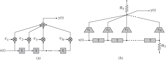
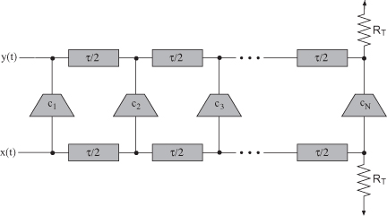
The transversal FIR filter topology is shown in Figure 21.6. Here a delay line is tapped at specific intervals (τ) to generate N delayed versions of the input signal x(t). These delayed versions are scaled by the tap weights ck and then combined to form an output y(t) of the form
(21.7)
![]()
where τ is the tap spacing. While Figure 21.6a describes the TVF topology in its most general form, Figure 21.6b illustrates the TVF topology as it would appear for a high-speed implementation [11]. The delay line is implemented using passive components and terminated to prevent reflections. The tap multipliers are implemented as transconductors, with the summation performed in the current domain.
Figure 21.6. Transversal FIR filter topology. (a) Conceptual block diagram. (b) High-speed implementation.
An FIR filter requires analog delays. A clock can be used to define the delay intervals [12], but its distribution with low skew and low jitter generally burns a lot of power. Alternately, analog continuous-time delays may be synthesized in two ways: using an artificial L-C transmission line or a microstrip transmission line. For a two-tap FIR implementation, a microstrip transmission line may be wrapped in a “U” shape, as shown in Figure 21.7a, making it simple to route both equalizer taps to a common summation node. This long narrow shape may be easier to fit in some receiver layouts. Since there are no inductors, it is easier to accommodate metal fill rules. Microstrip lines also have an inherently higher bandwidth due to their distributed nature. Whereas it is necessary to use special techniques to achieve baud-spacing with sufficient bandwidth due to the lumpiness of artificial transmission lines [13, 14], a single length of microstrip line can simply be used to achieve baud-rate tap spacing. This simplifies both the design and modeling of the interconnects.
Figure 21.7. Implementing a two-tap transversal FIR filter. (a) Transversal filter with microstrip line shaped as “U”. (b) Circuits chematic. (c) Die photo.
(Copyright IEEE 2008.)
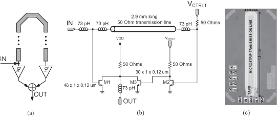
The schematic of a single-ended two-tap transversal FIR equalizer is shown in Figure 21.7b [15]. Common-source amplifiers are used as the tap transconductors. Located at the input of the equalizer, transistor M1 forms the first equalizer tap. The cascaded transistors M2 and M3 form the second tap of opposite polarity, a condition needed to create peaking. Signal inversion was performed with an additional common-source stage at the end of the transmission line instead of at the beginning to introduce additional signal delay, thus increasing the effective inter-tap delay and shortening the required transmission-line length. The majority of the inter-tap delay is provided by a 50-Ω microstrip transmission line that is terminated by a matching load resistor. In this design the tap outputs are summed in the current domain on a 50-Ω resistor which also provides output impedance matching, although a higher load resistance could have been used to provide high gain if driving on-chip loads only.
The die photo of the circuit is given in Figure 21.7c. Implemented in 130-nm CMOS, the size of the die excluding pads is 1.5 mm × 0.26 mm. The die includes a 2.9-mm-long, 9-µm-wide microstrip line that provides 18.2 ps of group delay and 50-Ω characteristic impedance and is laid out in a U-shaped fashion. In order to improve the input and output matching of the TVF, long narrow strips of metal each with 73-pH inductance are introduced around the nodes where the transconductors are connected.
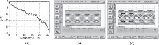
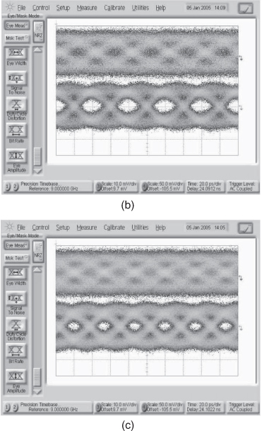
Eye diagram measurement results of the two-tap FIR filter are shown in Figure 21.8. Based on the channel frequency response shown in Figure 21.8a, a 38.2-Gbit/s signal experiences 14.3 dB of attenuation at one-half the bit rate (19.1 GHz). Figure 21.8b shows the closed and unequalized eye through the channel. Setting the tuning voltages VCTRL1 at 0.82 V and manually tuning the peaking control voltage VCTRL2 to 0.88 V, results in the equalized eye shown in Figure 21.8c. The chip consumes a maximum of 30 mW from a 1.2-V supply.
Figure 21.8. Measured 38.2-Gbit/s eye diagrams curve. (a) Frequency response of channel. (b) Unequalized eye: channel output. (c) Equalized eye: two-tap TVF output.
(Copyright IEEE 2008.)
21.4.2 Traveling-Wave FIR Filter Topology
The TVF topology discussed so far has two major disadvantages: Firstly, the outputs of the tap multipliers are tied together at the summation node. As a result, the capacitance at this node is very large and potentially speed-limiting. In addition, if the delay line is implemented using passive elements the inter-tap spacing may be quite large, making it physically difficult to tie these outputs together at a single node without introducing skew and signal degradation.
Secondly and more importantly, because the delay line is equal to the span of the equalizer, reflections that occur at the end of the delay line can be detrimental to the equalizer perform ance. For example, consider a three-tap symbol-spaced equalizer. A reflection at the end of the two-section delay line will traverse back to the first tap after four symbol periods. Thus, if ΓT is the reflection coefficient at the end of the delay line, the output will not be equal to (21.7), but rather
assuming that the
higher-order ΓT terms (![]() ,
, ![]() , etc.) are negligible. Therefore, the output contains terms
involving x(t − 4τ) and x(t − 3τ) that are outside the span of the
equalizer and that cannot be eliminated by adjusting the equalizer coefficients. In
effect, these terms serve to increase the ISI at the output [11]. An alternative
topology is the traveling-wave filter FIR topology that was first suggested in Jutzi
[16], and is shown in Figure 21.9. The main difference between this
topology and the TVF is that this topology makes use of delay lines at both the
input and the output. While the output y(t) is still given by Eq. (21.7), this topology addresses
some of the major issues with the TVF topology that arise at high speeds.
, etc.) are negligible. Therefore, the output contains terms
involving x(t − 4τ) and x(t − 3τ) that are outside the span of the
equalizer and that cannot be eliminated by adjusting the equalizer coefficients. In
effect, these terms serve to increase the ISI at the output [11]. An alternative
topology is the traveling-wave filter FIR topology that was first suggested in Jutzi
[16], and is shown in Figure 21.9. The main difference between this
topology and the TVF is that this topology makes use of delay lines at both the
input and the output. While the output y(t) is still given by Eq. (21.7), this topology addresses
some of the major issues with the TVF topology that arise at high speeds.
Figure 21.9. High-speed implementation of traveling-wave FIR filter topology.
First, there is no longer a lumped node at which all of the outputs are tied together. The capacitance at the inputs and outputs of the tap multipliers serve only to increase the capacitance of the input and output delay lines, respectively. In other words, the device capacitances are distributed along the length of the delay lines.
Also, this topology lends itself to an efficient layout because the inter-tap spacing is the same for both the input and output lines. The input and output lines can be laid out parallel to one another, with the tap multipliers interspersed between them.
Finally, this topology offers an improvement over the TVF in terms of robustness in the presence of reflections. Using the example of a three-tap filter, the output in the presence of reflections is
(21.9)
![]()
In contrast to Eq. (21.8), Eq.(21.9) does not contain any terms outside the span of the equalizer. Therefore, the extra x(t − 2τ) terms caused by the reflections can be compensated for by properly adjusting the weighting coefficient for the third equalizer tap [11].
Because of these benefits, many of the reported FFE implementations for EDC make use of the TWF topology [17–20].
TWF Design.
The basic TWF design is shown in Figure 21.9. The input and output transmission lines are chosen such that their characteristic impedance is matched to the system impedance and their delays implement the proper tap spacing. The input and output capacitances of the tap multipliers serve to capacitively load the input and output transmission lines, respectively. This loading effectively reduces the characteristic impedance of the transmission lines and must be considered in the design.
To achieve the required delays for a 40-Gbit/s equalizer, the transmission lines used in the input and output must be very long (on the order of several millimeters). As a result, the size of the equalizer IC can become prohibitively large. In addition, long transmission lines introduce significant series loss. For both of these reasons, it is desirable to minimize the length of these lines.
Using artificial transmission lines made up of lumped inductors and capacitors addresses both problems associated with distributed transmission lines. By winding the transmission line into spiral inductors, the inductance per unit length is greatly increased because of the mutual inductance between adjacent windings. Thus, the overall length of transmission line is decreased, reducing the chip area as well as any resistive losses.
The design of a TWF with artificial transmission lines is fairly straightforward, because most of the design variables are fixed by the desired configuration of the equalizer. The delays of the input and output transmission lines are determined by the desired tap spacing. The delay ΔT of a lumped L–C transmission line section is approximately equal to
(21.10)
![]()
where
L′ and C′ are the
inductance and capacitance of each section of the transmission line, respectively.
Also, the characteristic impedance of the input and output transmission lines (Z0) is determined by the system impedance (e.g., 50 ![]() ) and is
equal to
) and is
equal to
(21.11)
![]()
Substituting (21.11) into (21.10), we can solve for L′ and C′:
As an example,
consider a three-tap symbol-spaced equalizer operating at 40 Gbit/s with a system
impedance of 50 ![]() . The delay per transmission line section should
be TB/2, or 12.5 ps. Using Eqs. (21.12) and
(21.13),
L′ is equal to 625 pH and C′ is equal to 250 fF. The input and output capacitances of the tap
multipliers effectively add to the capacitance of the input and output transmission
lines, respectively. Therefore, C′ is made up of the sum
of the transmission line capacitances and the device capacitances. The termination
resistors RT are set equal to the system
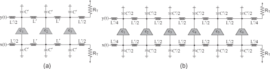
impedance. The resulting equalizer design is shown in Figure 21.10a. Note
that L′/2 inductors have been added to the ends of each
transmission line. This improves the symmetry of the transmission lines and ensures
that the total inductance (3L′) matches the total
capacitance (3C′).
. The delay per transmission line section should
be TB/2, or 12.5 ps. Using Eqs. (21.12) and
(21.13),
L′ is equal to 625 pH and C′ is equal to 250 fF. The input and output capacitances of the tap
multipliers effectively add to the capacitance of the input and output transmission
lines, respectively. Therefore, C′ is made up of the sum
of the transmission line capacitances and the device capacitances. The termination
resistors RT are set equal to the system
impedance. The resulting equalizer design is shown in Figure 21.10a. Note
that L′/2 inductors have been added to the ends of each
transmission line. This improves the symmetry of the transmission lines and ensures
that the total inductance (3L′) matches the total
capacitance (3C′).
Figure 21.10. TWF design. (a) Three-section input and output transmission lines. (b) Six-section input and output transmission lines.
The 3-dB bandwidth of an L–C section is equal to
(21.14)
![]()
For a TWF, the delay of each section, ΔT, is equal to one-half the tap spacing, or T/2. Thus, there is an inverse relationship between the bandwidth and the tap spacing of a TWF, as given by
(21.15)
![]()
For our example above, Eq. (21.15) yields a bandwidth of 25 GHz. This is insufficient for a 40-Gbit/s equalizer. To extend the bandwidth, the L–C stages must be made smaller, or the transmission line must be made less “lumpy.” Figure 21.10b shows an equalizer that is half as lumpy as the equalizer shown in Figure 21.10a.
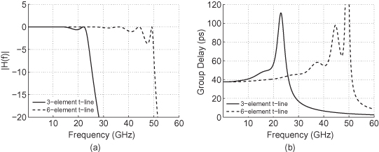
The bandwidth of each transmission line section is doubled to 50 GHz, using Eq. (21.14). Plots of the magnitude response and group delay for three- and six-section lumped transmission lines are given in Figure 21.11. These plots demonstrate the doubling of the bandwidth corresponding to a reduction of the lumpiness by a factor of two. From the group delay plots it is also observed that the group delay is flat only within the bandwidth of the transmission line, another important reason for making the transmission line more distributed.
Figure 21.11. Comparison between three- and six-element transmission lines. (a) Magnitude response. (b) Group delay.
(Copyright IEEE 2006.)
Note that since the node capacitances C′ are made up in part by the device capacitances, when C′ is scaled the device sizes must scale accordingly. Therefore, the gain through each stage of a six-section equalizer is only half that through each stage of a three-section equalizer, for the same equalizer span. Splitting the three gain cells into six gain cells effectively halves the maximum possible gain through any particular tap. This limits the performance of the equalizer for operation in the absence of channel impairments, when only one tap needs to be on, for example.
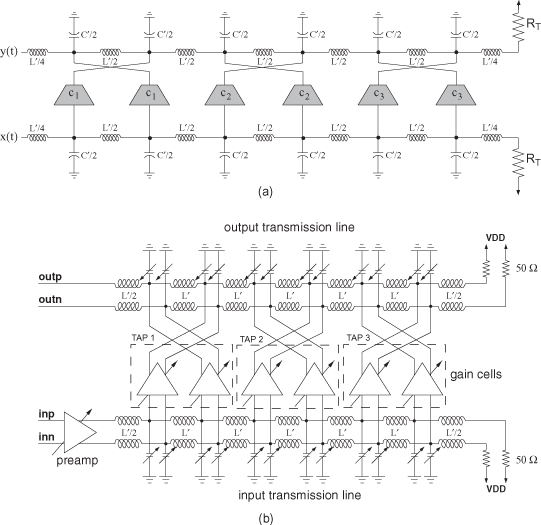
Crossover TWF Topology.
A slightly modified version of the TWF topology, which will be referred to as the crossover TWF topology, can be used to allow symbol-spaced equalization without increasing the lumpiness of the transmission lines or sacrificing any gain [13]. The crossover TWF topology is illustrated in Figure 21.12a.
Figure 21.12. Crossover TWF topology. (a) Three-tap equalizer using the crossover TWF topology. (b) Symbolic top-level circuit schematic for 90-nm equalizer IC.
(Copyright IEEE 2006.)
In Figure 21.12a, each L–C section is replaced with two sections having component values of L/2 and C/2 to maintain the same characteristic impedance. Thus each L–C section would have a delay ΔT equal to one-quarter of the tap spacing, or τ/4. Therefore, the bandwidth of the TWF would be given by
(21.16)
![]()
Hence, the delay through each section is halved while the bandwidth is increased. At data rates that push technologys limits, the capacitances C are comprised mostly of the transconductors’ parasitic input and output capacitances. Therefore, reducing these capacitances to C/2 implies scaling the size and of each transconductor by one-half. Fortunately, by crisscrossing outputs of consecutive transconductors, their gains add with equal group delay effectively forming a distributed amplier. Furthermore, each tap delay is now formed by four L–C sections (instead of two) giving the same tap spacing as the conventional TWF topology. Since this topology uses six-section transmission lines, it has a bandwidth given by Eq. (21.16), which is twice the bandwidth of the three-tap symbol-spaced equalizer described by Figure 21.10a.
A block diagram of the entire circuit is given in Figure 21.12b. A lumped preamplifier stage accepts differential inputs and performs a variable gain function to condition the input signal so as to maximize the dynamic range of the equalizer. It also performs a single-ended to differential conversion function when the circuit is driven by an unbalanced input. The preamplifier drives the differential 50-Ω input transmission line and consists of two cascaded differential pairs. A schematic of the lumped preamplifier stage is given in Figure 21.13a. The gain of the preamplifier stage is digitally-controllable. This gain control is provided both to allow tuning of the preamplifier bias currents for performance optimization and to allow compensation for possible variations in input power. The input and output transmission lines are made up of differential inductors and capacitances, and they generate the delays necessary in an FIR filter. Three gain cells tap this transmission line at intervals such that the difference in delay from one tap to the next is 25 ps (or one symbol period at 40 Gbit/s).
Figure 21.13. Circuit schematics. (a) Preamplifier block. (b) Variable gain cell.
(Copyright IEEE 2006.)
Each of the gain cells is composed of two differential pairs. The two differential pairs are connected with opposite polarity. This allows the filter to implement both positive and negative tap weights. To implement a positive tap weight, the bias current for the differential pair connected with negative polarity is first zeroed, leaving only the positive path from input to output. The gain in this positive path is controlled by adjusting the bias current of the differential pair connected with positive polarity. A negative tap weight is implemented using the converse of this procedure.
From Eq. (21.12), the inductance per element (L′) required for these transmission lines is 312.5 pH per side. From Eq. (21.13), the capacitance per element (C′) is 125 fF per side. The transmission lines contain six nodes, one for each gain cell. The capacitance at each of these nodes is C′. Between these six nodes are five inductances of L′ each. Inductances of L′/2 are added to each end of the transmission line so that the total inductance of the line is 6L′, which matches the total capacitance of 6C′.
The inductances L′are implemented by differential spiral inductors. The capacitances C′ at each node are composed of the device capacitances attached to the node supplemented by a variable capacitance created by a digitally controlled varactor. The varactor allows tuning of C′ to compensate for model inaccuracies and process variation. The characteristic impedance and delay can both be tuned by this varactor.
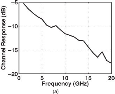
The equalizer was implemented in a 90-nm CMOS process. A die photo of the circuit layout is given in Figure 21.14a. The overall dimensions of the equalizer IC are 0.6 mm × 0.5 mm. All circuit measurements were made on wafer and were single-ended. Figure 21.14b shows the measured input and output return losses. Integrated 50-Ω resistors provided better than 16 dB of input return loss up to 30 GHz. The output return loss was better than only 9 dB up to 30 GHz. This is due to the mismatch in the characteristic impedance of the integrated delay line at the output and the measurement instruments as a consequence of larger-than-estimated node capacitance of the delay lines. Figure 21.14c shows the tap spacing measured at 10 GHz which was obtained by measuring each tap separately on an oscilloscope and superimposing the traces. The measured tap spacing was 37 ps, which was considerably larger than the 25 ps targeted for the filter design. Again this was due to larger-than-estimated node capacitances of the delay lines. For equalization experiments, a lossy channel was constructed with coaxial cables, connectors, and an attenuator. The response of the channel is shown in Figure 21.15a. Input and output eyes to the equalizer are shown in Figures 21.15b and 21.15c for data data rates of 25 Gbit/s and 30 Gbit/s.
Figure 21.14. TWF crossover topology. (a) Die photo. (b) Measured input and output return loss. (c) Measured tap response for a 10-GHz sinusoid.
(Copyright IEEE 2006.)
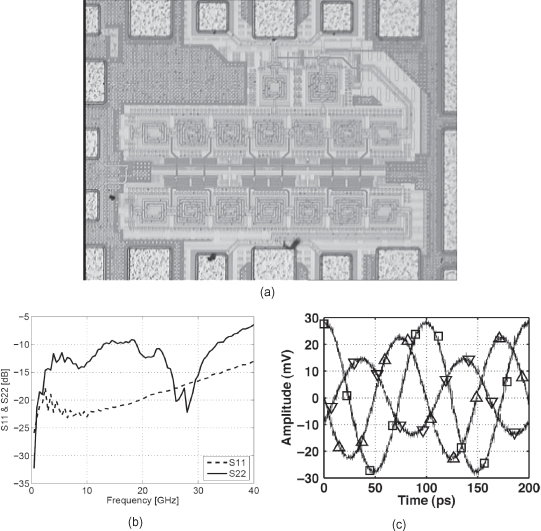
Figure 21.15. Time domain measurements for TWF crossover topology. (a) Channel Response. (b) Measured input and output eyes at 25 Gbit/s. (c) Measured input and output eyes at 30 Gbit/s.
(Copyright IEEE 2006.)
The equalizer consumes approximately 25 mW from a 1-V supply. This is significantly lower than both of the 40-Gbit/s FFEs previously reported (820 mW [19] and 750 mW [20]) and nearly all of the 10-Gbit/s FFEs previously reported.
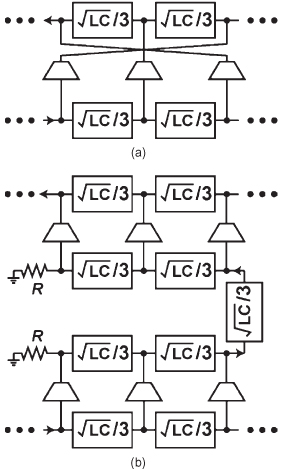
Folded-Cascade TWF Topology.
The crossover TWF topology allows the implementation of a symbol-spaced equalizer as a TWF while decreasing the lumpiness of the transmission lines by a factor of two. It is not practical, however, to decrease the lumpiness of the transmission lines by a factor greater than two using the crossover TWF topology. The crossover routing between two taps cannot easily be reproduced for three or more taps without introducing asymmetries and skew between the different paths.
Theoretically, it should be possible to increase the bandwidth of the crossover TWF topology by further subdividing the delay lines and using more than two ampliers per tap. For instance, Figure 21.16a shows a single tap of a crossover TWF using three ampliers per tap. Unfortunately, the crossover routing is no longer symmetric. The resulting mismatch and skew between the paths of different length may introduce unacceptable ripple into the frequency response. By using an intermediate folded transmission line to perform the crossover routing minimal delay mismatch can be achieved as shown in Figure 21.16b. The tap spacing is the same as in Figure 21.16a. The delay lines are all composed of one-third-sized L–C sections, so that the bandwidth is three times greater than a conventional TWF for the same tap spacing. Thus if each tap of a symbol-spaced folded-cascade TWF is composed of two cascaded stages of M gain elements each, the bandwidth of the equalizer is given by
(21.17)
![]()
Figure 21.16. Evolution of the folded cascade TWF. (a) Using three amplifiers per tap to boost the bandwidth. (b) Using a cascade of two distributed amplifiers per tap to boost the bandwidth.
(Copyright IEEE 2006.)
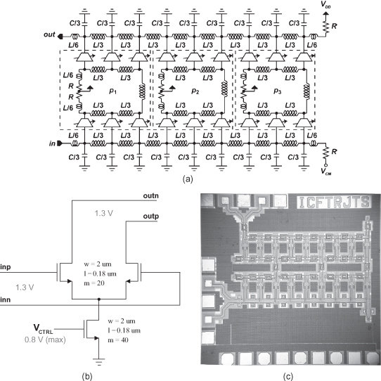
Using this topology results in the three-tap FIR
filter of Figure 21.17a [14]. Note that any two paths through neighboring tap amplifiers
differ in length by six L–C
sections. Hence, the tap spacing is ![]() ,
just as in the conventional and the crossover TWF topology. The values for the
inductance of L/3 and capacitance C/3 of each transmission line section are calculated to provide a
characteristic impedance of 50
,
just as in the conventional and the crossover TWF topology. The values for the
inductance of L/3 and capacitance C/3 of each transmission line section are calculated to provide a
characteristic impedance of 50 ![]() per side (100
per side (100 ![]() differential) and a tap spacing of 25 ps (one bit period at 40 Gbit/s). Since the
tap spacing is determined by six L–C sections,
differential) and a tap spacing of 25 ps (one bit period at 40 Gbit/s). Since the
tap spacing is determined by six L–C sections, ![]() must equal
to one-sixth of a bit period, or 4.17 ps. The resulting values of L/3 and C/3 are 209 pH and 83
fF per side, respectively. The node capacitances are made up purely of transistor
and inductor parasitics. The inductances are spiral coils. Additional half-sized
inductors L/6 = 105 pH are required at the ends of each
transmission line as shown in Figure 21.17a. The gain cell used in this equalizer
is a differential pair, as shown in Figure 21.17b. Six of these differential pairs make
up each of the three equalizer taps. Each of the three taps has a fixed polarity.
The first tap is positive, the second is negative, and the third is positive. These
polarities correspond to a high-pass response, which would be the typical response
of such an equalizer when used with most chip-to-chip or PMD channels. The filter
was implemented in 180-nm CMOS. A die photo of the circuit layout is given in Figure
21.17c.
The overall dimensions of the equalizer IC are 1 mm × 1 mm.
must equal
to one-sixth of a bit period, or 4.17 ps. The resulting values of L/3 and C/3 are 209 pH and 83
fF per side, respectively. The node capacitances are made up purely of transistor
and inductor parasitics. The inductances are spiral coils. Additional half-sized
inductors L/6 = 105 pH are required at the ends of each
transmission line as shown in Figure 21.17a. The gain cell used in this equalizer
is a differential pair, as shown in Figure 21.17b. Six of these differential pairs make
up each of the three equalizer taps. Each of the three taps has a fixed polarity.
The first tap is positive, the second is negative, and the third is positive. These
polarities correspond to a high-pass response, which would be the typical response
of such an equalizer when used with most chip-to-chip or PMD channels. The filter
was implemented in 180-nm CMOS. A die photo of the circuit layout is given in Figure
21.17c.
The overall dimensions of the equalizer IC are 1 mm × 1 mm.
Figure 21.17. FIR filter topology. (a) Three-tap folded cascade TWF filter with programmable gains. (b) Schematic of equalizer gain cell. (c) Die photo of 0.18-µm equalizer.
(Copyright IEEE 2006.)
All circuit measurements were made on-wafer. Figure 21.18a shows the output of the filter with a 10-GHz sinusoidal input. The measurement was made by turning on each tap individually, with all other taps turned off. The tap spacing is 23 ps, just under one baud interval at 40 Gbit/s. Note that the polarity of tap 2 is reversed compared with taps 1 and 3. Figures 21.18b and 21.18c plot the magnitude of the input and output return losses, respectively, both simulated and measured with a two-port network analyzer. The input return loss is greater than 15 dB from 5 to 40 GHz, while the output return loss is better than 16 dB up to 40 GHz. A 4-m coaxial cable was used for eye diagram measurements. Figure 21.19a plots the frequency response of the cable along with the frequency response of a PMD limited channel model with γ = 0.4 and Δτ = 25 ps and transmitter and receiver bandwidths of 25 GHz. Figure 21.19b shows a 40-Gbit/s single ended unequalized eye pattern at the end of the 4-m cable. The measured output eyes are shown in Figure 21.19c and 21.19d at 30 Gbit/s and 40 Gbit/s respectively.
Figure 21.18. FIR filter measurements. (a) Measured tap delays with a 200-mV peak-to-peak 10 GHz sinusoidal input. (b) Measured (solid) and simulated (dashed) input return loss. (c) Measured (solid) and simulated (dashed) output return loss.
(Copyright IEEE 2006.)
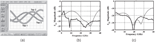
Figure 21.19. Eye diagram measurements. (a) Measured cable frequency response (solid) along with the modeled response of PMD channel with γ = 0.4 and Δτ = 25 ps (dashed). (b) Channel output (equalizer input) at 40 Gbit/s. (c) Equalizer output at 30 Gbit/s. (d) Equalizer output at 40 Gbit/s.
(Copyright IEEE 2006.)
Research on broadband FIR equalizers is ongoing and active. This section has discussed topologies that distribute parasitic capacitances along L–C delay lines [13, 14]. Low-power FIR architectures are shown in Tiruvuru and Pavan [21]. Others have employed small active circuits to mitigate losses in passive delay lines [22]. Research on these topics will no doubt continue; but for longer links and/or higher data-rates, more sophisticated methods for EDC are being researched.
21.5 IIR FILTERS FOR EDC
This section considers the use of traveling-wave filter techniques for the implementation of an infinite impulse response (IIR) filter. Figure 21.20a shows a top-level block diagram of a direct form 2-tap IIR filter that uses a traveling-wave topology with only poles in its transfer function. Due to the absence of a feed-forward path, zeros are eliminated from the transfer function of the filter, thus simplifying the hardware required to implement the filter. The total loop delay from the input to the output through the first tap a1 is τ, and the total loop delay from the input to the output through the second tap a2 is 2τ. Ideally the frequency at which peaking is observed in the magnitude response of the all-pole IIR filter is given by
(21.18)
![]()
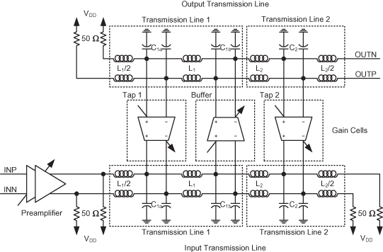
where τd is the total delay around a feedback loop that includes an active tap amplifier. Thus, ideally tap a1 produces a peak at 1/(2τ), whereas tap a2 produces a peak at 1/(4τ). A drawback of the direct-form all-pole IIR topology is the double peaking behavior observed when utilizing the low-frequency tap, a2, with the high-frequency tap, a1, turned off. This arises from the periodic nature of the filter peaks and the finite bandwidth of the delay line segments. Moreover, with the high-frequency peak at twice as large as the low-frequency peak, it becomes difficult to place both peaks within the frequency band of interest. Practically, it would be desirable to bring the low- and high-frequency peaks close enough to each other to permit them to create a single peak, providing frequency boosting over a broader range. To bring the peak frequencies closer, the direct-form all-pole IIR can be modified into the multi-delay IIR section as shown in Figure 21.20b. Here delay section τ1 determines the peak location for tap a1, while delay section τ1 + τ2 determines the peak location for tap a2. By allowing different segment delays, the multi-delay IIR filter allows two peak frequencies to be placed in close proximity to each other while suppressing any undesired secondary peak with the low-frequency tap on. A major drawback of this topology is that τ2 cannot be selected independently from τ1. Consequently, the delay τ2 would be forced to be small in order to bring the peaking frequencies close together. To alleviate this problem, the multi-delay IIR filter can be modified as shown in Figure 21.20c to form a double loop. By introducing two independent feedback loops, the delays τ1 and τ2 can be sized independently according to the desired peak frequencies. Figure 21.21 shows the top-level block diagram of the double-loop multi-delay all-pole IIR filter that uses a traveling-wave architecture [23]. The filter delays are realized using lumped L–C transmission sections. The loop containing transmission line 1, tap1, and buffer forms the low-frequency peaking path, while the loop containing transmission line 2, tap2, and buffer forms the high-frequency peaking path. Both transmission line segments were designed to have 50-Ω characteristic impedance. The first segment, transmission line 1, is designed to have 9.375-ps delay. Using Eqs. (21.12) and (21.13), initial values for L1 and C1a (or C1b) were chosen as 468 pH and 178 fF, respectively. Similarly, transmission line 2 is designed to have 5-ps delay resulting in 250 pH and 100 fF for L2 and C2, respectively. The filter utilizes two differently sized gain cells. The center buffer gain cell is larger than the feedback gain cells. The gain cells are sized such that device and parasitic capacitances account for a maximum of 60% of the total node capacitance. The final values of inductance and capacitances were: L1 = 370.1 pH, L2 = 220.1 pH, C1a = 79.6 fF, C1b = 35.4 fF, and C2 = 26 fF. A lumped two-stage preamplifier that is matched to a 100-Ω differential system impedance precedes the filter. The tail currents of the preamplifier and the gain cells were made adjustable through current mirrors to control their gains.
Figure 21.20. All pole traveling wave IIR filter topologies. (a) Direct form (uniform delay). (b) Multi-delay. (c) Double loop multi-delay.
(Copyright IEEE 2009.)
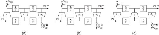
Figure 21.21. Top-level schematic of the double-loop multi-delay IIR TWF equalizer.
(Copyright IEEE 2009.)
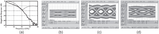
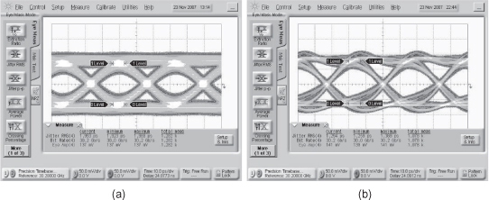
The IIR filter was implemented in a 90-nm CMOS process and occupied an area of 0.85 mm × 0.625 mm. Figure 21.22 shows the die photo. All circuit measurements were done on wafer. Figure 21.23 plots the measured S-parameters of the filter with both taps on. The filter produces a 12.1-dB peak at 24 GHz. Under these conditions the filter consumes 55.2 mW from a 1.2-V supply. 30-Gbit/s eye diagrams at the filter input and output are shown in Figure 21.24.
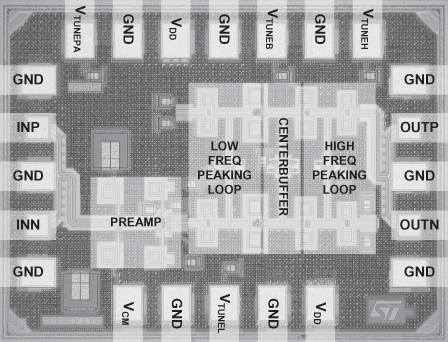
Figure 21.23. Measured examples of mixed peaking. VTUNEL = 0 V, VTUNEH = 0.4 V; S21 (circle), S11 (triangle), S22 (square).
(Copyright IEEE 2009.)
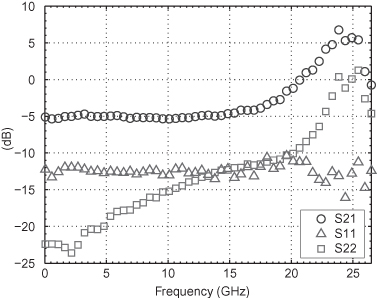
Figure 21.24. Measured 30.2-Gbit/s channel equalization. (a) Unequalized eye input to the filter. (b) Equalized eye output of the filter.
21.6 ELECTRONIC DISPERSION COMPENSATION USING NONLINEAR EQUALIZATION: DECISION FEEDBACK EQUALIZATION (DFE)
Ultimately, if the channel has deep nulls in its frequency response, linear equalization is insufficient. Some form of nonlinear processing is required to restore the lost portion of transmitted spectrum. The most common examples are decision feedback equalization and maximum likelihood sequence estimation. A decision feedback equalizer (DFE) is a nonlinear receiver that can restore lost portions of transmit spectrum using past decisions. A DFE does not significantly amplify the system noise because it outputs a digital decision instead of an analog voltage. For most practical systems, a DFE is often paired with a feed-forward equalizer (FFE) to correct for a variety of channels.
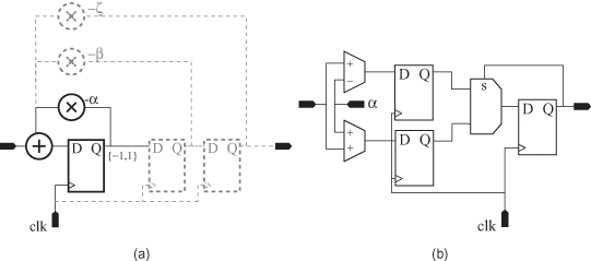
The direct feedback equalizer is the conventional approach to implementing a DFE as shown in Figure 21.25a. The filter processing is computed in the feedback path and added at the summing node. The implementation allows for multiple taps to be added as seen in Figure 21.25a by the inclusion of the dotted components. From a system viewpoint, direct feedback equalizers still allow for a well-known proven clock and data recovery (CDR) circuit to be used with little added overhead for clock distribution. The major drawback, however, involves the timing bottleneck of the feedback path which must be completed within a bit period. To shorten this critical path and enable higher-speed operation, parallel processing can be employed in a “speculative” or “look-ahead” DFE architecture [24]. By removing the filter stages in the feedback path of the direct form equalizer in Figure 21.25a, the timing constraints are relaxed in the look-ahead architecture shown in Figure 21.25b. The look-ahead architecture equalizes the input signal making multiple decisions. One path makes a tentative decision assuming that the previous bit was a 1, and the other path assumes that the previous bit was a 0. The correct result is then selected, and the other decision is discarded via a decision-selective feedback (DSF) loop. This relaxes the timing constraint within the filter processing as well as removes the summing node for multiple tap designs allowing for high-speed implementation. The addition of the look-ahead architecture, however, complicates the overall system by increasing the complexity of the CDR circuit as well as the clock distribution. This results in an overall increase in the area and power consumption. This technique has been demonstrated in silicon at data rates up to 40 Gbit/s [25].
Figure 21.25. DFE architectures. (a) Direct feedback architecture. (b) Look-ahead architecture reported in references 24 and 25.
DFEs can also be realized in the digital domain. This would require an ADC front end to convert the incoming analog signal to a digital signal. The digital signal can then be sent to an FFE in cascade with a DFE. The clock recovery would also be performed digitally. This type of DSP-based architecture has been reported for an MMF link at 10-Gbit/s in 65-nm CMOS [26]. Note that DSP-based transceivers provide robust performance in the presence of severe channel impairments and can be easily scaled with the process, thus resulting in reduced power and area.
21.7 ALTERNATIVE APPROACHES TO DISPERSION COMPENSATION
There are many other alternatives to dispersion compensation. From a research perspective, two of the most noteworthy approaches are discussed here.
21.7.1 Maximum Likelihood Sequence Estimation (MLSE)-Based Receiver
Maximum likelihood sequence estimation (MLSE) recognizes specific patterns of ISI and uses them to inform its decision. This is superior to a DFE-based receiver since a DFE essentially “throws away” signal energy by canceling post-cursor ISI. For example, Figure 21.26 shows a performance improvement of roughly 1.5 dB for an ideal implementation of MLSE compared with a two-tap DFE. However, the ideal implementation of MLSE implies perfect a priori knowledge of the channel response at the receiver and signal detection using the energy from the entire pulse response. The complexity of such an implementation would be massive compared to a DFE implementation.
Figure 21.26. Bit error rate versus SNR for the split-pulse channel response in Fig. 21.3c using a six-tap 1/2-UI-spaced linear equalizer, a DFE comprising the same six-tap 1/2-UI-spaced linear equalizer with a two-tap feedback equalizer, and an MLSE receiver.
(Copyright IEEE 2008.)
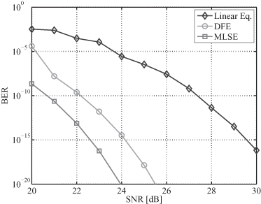
A partial response maximum likelihood (PRML) receiver employs a linear equalizer preceding MLSE to partially equalize the channel response. This results in a shorter channel pulse response that can be processed by an MLSE with practical complexity. However, the performance of a PRML receiver lies somewhere between that of the DFE and ideal MLSE as shown in Figure 21.26, which is due to the noise amplification and correlation of the linear equalizer. Fortunately, noise amplification is minimized and performance close to that of ideal MLSE is obtainable if the partial response target can be chosen to closely match the channel’s inherent response.
The Viterbi algorithm is a practical realization of MLSE. Analog implementations of the Viterbi algorithm have been reported for relatively short partial response targets at data rates of hundreds of Mbps [27]. However, most research effort on MLSE receivers at 10 Gbit/s has focused on digital implementations for two main reasons. Firstly, analog Viterbi detectors were not well-suited to the longer and adaptive partial response targets sought in optical communication applications. Secondly, advancing CMOS process technologies favor mostly digital architectures. Hence, it would seem that a digital receiver is the ultimate solution for EDC provided that a suitable ADC can be designed. Digital MLSE receivers have already been reported [28]. The current state of the art provides 4- to 6-bit ADCs for 10-Gbit/s systems, but research towards 40 Gbit/s systems is ongoing, with the required ADC having already been demonstrated [29].
21.7.2 Adaptive Optics in Dispersion Compensation
Multiple transmit and receive antennas can be used to combat multipath fading in wireless links. Similarly, multiple lasers and photodetectors can be employed to turn a single optical fiber into a multiple-input multiple-output (MIMO) communication channel with an attendant increase in channel capacity [30]. At the transmitter, the light source is spatially modulated and confined to only one mode of propagation in order to maintain signal integrity [31]. At the receiver, “spatial equalization” is achieved by combining the outputs of an array of photdetectors and canceling interfering propagation modes [32]. Whether at the transmitter or receiver, the optics must be adapted to track time variations in the channel.
Although promising, this avenue of research is still in early stages. Segmented light sources and detectors that are robust and inexpensive are still needed. Advances in signal processing are also required because MIMO methods are currently limited to wireless communication operating at a small fraction of the data rates in optical fiber links.
21.8 CONCLUSION
Dispersion is a major impairment in optical fibers that needs to be compensated in order to achieve high data rates. Integrated circuits can provide cost-effective and adaptive solutions to dispersion compensation by employing improved versions of well-known equalizer topologies. Both linear and nonlinear equalizers were discussed in this chapter. Linear equalizers provide high-frequency boost and are typically implemented using finite impulse response (FIR) or infinite impulse response (IIR) filters. Implementation and measurement results of various FIR filters are presented in Section 21.4. An example of an IIR filter is presented in Section 21.5 with measurement results. Nonlinear architectures such as DFEs are suitable for removing nulls in the frequency response and are presented in Section 21.6. However, these solutions just scratch the surface on EDC, and several difficult challenges are not even touched upon. For instance, adaptation and timing recovery are two key issues that need to be explored. A complete solution to the problem of dispersion is the key to developing reliable broadband and long-reach communication systems.
REFERENCES
1. P. Pepeljugoski, S. E. Golowich, A. J. Ritger, P. Kolesar, and A. Risteski, Modeling and simulation of next-generation multimode fiber links, J. Lightwave Technol., Vol. 21, No. 5, pp. 1242–1255, May 2003.
2. B. Razavi, Design of Integrated Circuits for Optical Communications, McGraw-Hill, New York, 2003.
3. C. D. Poole, R. W. Tkach, A. R. Chraplyvy, and D. A. Fishman, Fading in lightwave systems due to polarization-mode dispersion, IEEE Photon. Technol. Lett., Vol. 3, No. 1, pp. 68–70, January 1991.
4. H. Bülow, Operation of digital optical transmission system with minimal degradation due to polarisation mode dispersion, Electron. Lett., Vol. 31, No. 3, pp. 214–215, 1995.
5. G. J. Foschini and C. D. Poole, Statistical-theory of polarization dispersion in single-mode fibers, J. Lightwave Technol., Vol. 9, No. 11, pp. 1439–1456, November 1991.
6. N. Gisin, R. Passy, J. C. Bishoff, and B. Perny, Experimental investigations of the statistical properties of polarization mode dispersion in single mode fibers, IEEE Photon. Technol. Lett., Vol. 5, No. 7, pp. 819–821, July 1993.
7. H. Bülow, W. Baumert, H. Schmuck, F. Mohr, T. Schulz, F. Kuppers, and W. Weiershausen, Measurement of the maximum speed of PMD fluctuation in installed field fiber, in Optical Fiber Communication Conference, 1999, and the International Conference on Integrated Optics and Optical Fiber Communication. OFC/IOOC ’99. Technical Digest, Vol. 2, 1999, pp. 83–85.
8. R. Ramaswami and K. N. Sivarajan, Optical Networks—A Practical Perspective, 2nd edition, Morgan Kaufmann Publishers, San Francisco, 2002.
9. F. Buchali and H. Bülow, Adaptive PMD compensation by electrical and optical techniques, J. Lightwave Technol., Vol. 22, No. 4, pp. 1116–1126, Apri1 2004.
10. H. Bülow, Polarisation mode dispersion (PMD) sensitivity of a 10 Gbit/s transmission system, in Optical Communication, 1996. ECOC ’96. 22nd European Conference on, Vol. 2, 1996, pp. 211–214.
11. S. Pavan, Continuous-time integrated FIR filters at microwave frequencies, IEEE Trans. Circuits Syst. II, Vol. 51, No. 1, pp. 15–20, January 2004.
12. J. Jaussi, G. Balamurugan, D. Johnson, B. Casper, A. Martin, J. Kennedy, N. Shanbhag, and R. Mooney, 8-Gb/s source-synchronous I/O link with adaptive receiver equalization, offset cancellation, and clock de-skew, IEEE J. Solid-State Circuits, Vol. 40, No. 1, pp. 80–88, January 2005.
13. J. Sewter and A. Chan Carusone, A CMOS finite impulse response filter with a crossover traveling wave topology for equalization up to 30 Gb/s, IEEE J. Solid-State Circuits, Vol. 41, No. 4, pp. 909–917, April 2006.
14. J. Sewter and A. Chan Carusone, A 3-tap FIR filter with cascaded distributed tap amplifiers for equalization up to 40 Gb/s in 0.18-µm CMOS, IEEE J. Solid-State Circuits, Vol. 41, No. 8, pp. 1919–1929, August 2006.
15. G. Ng and A. C. Carusone, A 38-Gb/s 2-tap transversal equalizer in 0.13-µm CMOS using a microstrip delay element, in IEEE RFIC Conference, Atlanta, Georgia, June 2008.
16. W. Jutzi, Microwave bandwidth active transversal filter concept with MESFETs, IEEE Trans. Microwave Theory Tech., Vol. MTT-19, No. 9, pp. 760–767, September 1971.
17. H. Wu, J. A. Tierno, P. Pepeljugoski, J. Schaub, S. Gowda, J. A. Kash, and A. Hajimiri, Integrated transversal equalizers in high-speed fiber-optic systems, IEEE J. Solid-State Circuits, Vol. 38, No. 12, pp. 2131–2137, December 2003.
18. C. Pelard, E. Gebara, A. J. Kim, M. G. Vrazel, F. Bien, Y. Hur, M. Maeng, S. Chandramouli, C. Chun, S. Bajekal, S. E. Ralph, B. Schmukler, V. M. Hietala, and J. Laskar, Realization of multigigabit channel equalization and crosstalk cancellation integrated circuits, IEEE J. Solid-State Circuits, Vol. 39, No. 10, pp. 1659–1670, October 2004.
19. M. Nakamura, H. Nosaka, M. Ida, K. Kurishima, and M. Tokumitsu, Electrical PMD equalizer ICs for a 40-Gbit/s transmission, in Optical Fiber Communication Conference and Exhibit, 2004, OFC 2004, Vol. TuG4, 2004.
20. A. Hazneci and S. P. Voinigescu, A 49-Gb/s, 7-tap transversal filter in 0.18 µm SiGe BiCMOS for backplane equalization, in IEEE Compound Semiconductor Integrated Circuits Symposium, Monterey, CA, October 2004.
21. R. Tiruvuru and S. Pavan, Transmission line basd FIR structures for high speed adaptive equalization, in IEEE International Symposium on Circuits and Systems, Kos, Greece, May 2006, pp. 1051–1054.
22. S. Reynolds, P. Pepeljugoski, J. Schaub, J. Tiemo, and D. Beisser, A 7-tap transverse analog-fir filter in 0.13 µm CMOS for equalization of 10 Gb/s fiber-optic data systems, in IEEE ISSCC Digest Technical Papers, February 2005, pp. 330–331.
23. G. Ng, F. A. Musa, and A. C. Carusone, A 2-tap traveling wave infinite impulse response (IIR) filter with 12-dB peaking at 24-GHz, Electron. Lett., Vol. 45, No. 9, pp. 463–464, 2009.
24. S. Kasturia and J. H. Winters, Techniques for high-speed implementation of nonlinear cancellation, IEEE J. Selected Areas Commun., Vol. 9, No. 5, pp. 711–717, June 1991.
25. A. Garg, A. Chan Carusone, and S. P. Voinigescu, A 1-tap 40-Gbps look-ahead decision feedback equalizer in 0.18-µm SiGe BiCMOS technology, IEEE J. Solid-State Circuits, Vol. 41, No. 10, pp. 2224–2232, October 2006.
26. J. Cao, B. Zhang, U. Singh, D. Cui, A. Vasani, A. Garg, W. Zhang, N. Kocaman, D. Pi, B. Raghavan, H. Pan, I. Fujimori, and A. Momtaz, A 500 mw digitally calibrated AFE in 65 nm CMOS for 10 Gb/s serial links over backplane and multimode fiber, in Solid-State Circuits Conference, 2009, Digest of Technical Papers, ISSCC. 2009 IEEE International, 2009, pp. 370–371.
27. B. Zand and D. Johns, High-speed CMOS analog Viterbi detector for 4-PAM partial-response signaling, IEEE J. Solid-State Circuits, Vol. 37, No. 7, pp. 895–903, July 2002.
28. H. min Bae, J. Ashbrook, J. Park, N. Shanbhag, A. Singer, and S. Chopra, An MLSE receiver for electronic-dispersion compensation of OC-192 fiber links, in International Solid-State Circuits Conference, Digest of Technical Papers, San Francisco, CA, February 2006, pp. 874–883.
29. S. Shahramian, S. P. Voinigescu, A. Chan Carusone, “A 35-GS/s, 4-bit flash ADC with Active Data and Clock Distribution Trees,” IEEE Journal of Solid-State Circuits, Vol. 44, Issue. 6, pp. 1709–1720, June 2009.
30. H. Stuart, Dispersive multiplexing in multimode optical fiber, Science, Vol. 289, No. 5477, pp. 281–283, July 2000.
31. J. Kahn, Compensating multimode fiber dispersion using adaptive optics, in Optical Fiber Conference, Anaheim, California, March 2007, p. OTuL1.
32. K. Patel, A. Polley, K. Balemarthy, and S. Ralph, Spatially resolved detection and equalization of modal dispersion limited multimode fiber links, J. Lightwave Technol., Vol. 24, No. 7, pp. 2629–2636, July 2006.