Chapter 8. Adding Peripherals Using I2C
Perfection is achieved, not when there is nothing more to add, but when there is nothing left to take away.
—Antoine de Saint-Exupéry
In the last chapter, we looked at the low-cost SPI interface used to connect peripheral chips to microcontrollers. In this chapter, we’ll examine the alternate serial interface for connecting peripherals, I2C.
Overview of I2C
I 2 C (Inter-Integrated Circuit) bus is a very cheap yet effective network used to interconnect peripheral devices within small-scale embedded systems. It is sometimes also known as IIC and has been in existence for more than 20 years. It is the equivalent of SPI, but its operation is somewhat different.
I2C uses two wires to connect multiple devices in a multi-drop bus. The bus is bidirectional, low-speed, and synchronous to a common clock. Devices may be attached or detached from the I2C bus without affecting other devices. Several manufacturers, such as Microchip, Philips, Intel, and others produce small microcontrollers with I2C built in. The data rate of I2C is somewhat slower than SPI, at 100 kbps in standard mode, and 400 kbps in fast mode.
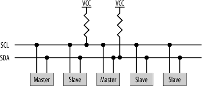
The two wires used to interconnect with I2C are SDA (serial data) and SCL (serial clock). Both lines are open-drain.[*] They are connected to a positive supply via a pull-up resistor and therefore remain high when not in use. A device using the I2C bus to communicate drives the lines low or leaves them pulled high as appropriate. Each device connected to the I2C bus has a unique address and can operate as either a transmitter (a bus master), a receiver (a bus slave), or both (Figure 8-1). I2C is a multi-master bus , meaning that more than one device may assume the role of bus master.
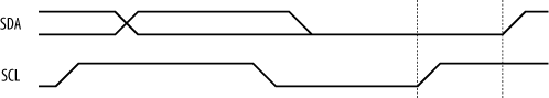
Both SDA and SCL are bidirectional. Unlike SPI, which has separate data lines for each direction of communication, I2C shares the same signal line for master transmission and slave response. Also unlike SPI, I2C does not have several modes of operation. The timing relationship between the clock, SCL, and the data line, SDA, is simple and straightforward. When idle, both SDA and SCL are high. An I2C transaction begins with SDA going low, followed by SCL (Figure 8-2). This indicates to all receivers on the bus that a packet transmission is commencing. While SCL is low, SDA transitions (high or low) for the first valid data bit. This is known as a “START condition.”
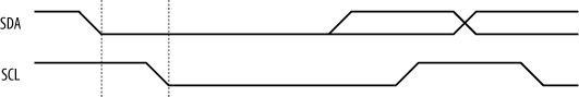
For each bit that is transmitted, the bit must become valid on SDA while SCL is low. The bit is sampled on the rising edge of SCL and must remain valid until SCL goes low once more. Then SDA transitions to the next bit before SCL goes high once more (Figure 8-3).
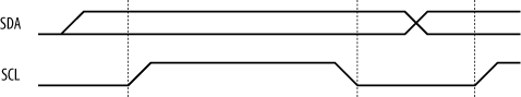
Finally, the transaction completes by SCL returning high (inactive) followed by SDA (Figure 8-4). This is known as a “STOP condition.”
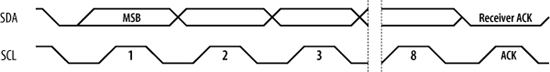
Any number of bytes may be transmitted in an I2C packet. As with SPI, the most significant bit of the packet is transmitted first. If the receiver is unable to accept any more bytes, it can abort the transmission by holding SCL low. This forces the transmitter to wait until SCL is released again.
Each byte transmitted must be acknowledged by the receiver. Upon the transmission of the eighth data bit, the master releases the data line SDA. The master then generates an additional clock pulse on SCL. This triggers the receiver to acknowledge the byte by pulling SDA low (Figure 8-5). If the receiver fails to pull SDA low, the master aborts the transfer and takes appropriate error-handling measures.
Now, I2C is a multi-master bus. So, more than one master may attempt to start transmission at the same time. Since the bus’s default state is high, a master transmitting a 0 bit will pull SDA low but will leave the bus in its default state if the bit is to be a 1. Thus, if two masters begin simultaneous transmission, a master leaving the bus in its default state for a 1 bit, but detecting the bus pulled low by another master (for a 0 bit), will register an error condition and abort the transmission.
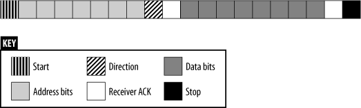
SPI uses a separate chip select to enable a receiving slave. Each SPI slave has a separate chip select that is generated by the master. I2C does not have such a selection mechanism. Instead, each device on the bus has a unique address, and the packet transmission begins with address bits, followed by the data. An address byte consists of seven address bits, followed by a direction bit. If the direction bit is a 0, the transmission is a write cycle and the selected slave will accept the data as input. If the direction bit is a 1, then the request is for the slave to transfer data back to the master. A sample packet, transferring one byte of data, is shown in Figure 8-6.
There is a special address, known as the general call address
, which broadcasts to all I2C devices. This address is %0000000 with a direction bit of 0. The general call is the mechanism by which the master determines what slaves are available, and there are several types of general call. The second byte of a general call indicates the purpose of the general call to the slaves. Upon receiving the second byte, individual slaves will determine whether the command is applicable to them, and, if so, they will acknowledge. If the command is not applicable to a given slave, then the slave simply ignores the general call and does not acknowledge. If the second byte is 0x06 (%00000110), then this indicates that appropriate slaves should reset and respond with their addresses. If the second byte is 0x04 (%00000100), slaves respond with their addresses but do not reset. Any other second byte of a general call, where the least significant bit is a 0, should be ignored.
If the least significant bit of the second byte is a 1, then the general call is by a master device identifying itself to other masters in the system by transmitting its own address. The other bits of the second byte contain the master’s address.
There is another special address byte, known as the START byte
. This byte is %00000001 (0x01). It is used to indicate to other masters that a long data transfer is beginning. This is particularly important for masters that do not have dedicated I2C hardware and must monitor the bus by software polling. When a master detects a START byte generated by another master, it can reduce its polling rate, allowing it more time for other software tasks.
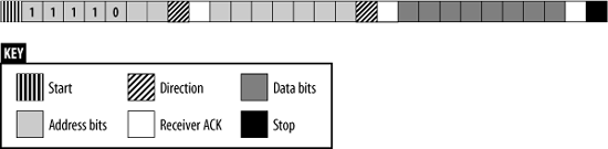
I2C also supports an extended 10-bit addressing mode, allowing up to 1,024 peripherals. Devices that use 7-bit addressing may be mixed with 10-bit addressing devices in a single system. In 10-bit addressing, two bytes are used to hold the address. If the (first) address byte begins with %11110XX, then a 10-bit address is being generated. The two least significant bits of the first byte, combined with the eight bits of the second byte, form the 10-bit address (Figure 8-7). 7-bit devices will ignore the transaction.
Adding a Real-Time Clock with I2C
We saw in the previous chapter how to interface a Real-Time Clock (RTC) to a microprocessor using a SPI interface. Now let’s look at how we’d do the same using the I2C interface. For this example, we’ll use the tiny Philips PCF8583. It also has 240 bytes of RAM, which, like the DS1305, may be used for parameter storage. Unlike the DS1305, it does not have an integrated battery-backup system. So, you would need to provide an external battery-backup circuit. There are many other I2C RTCs available, and some do incorporate battery-fail protection. I’ve chosen to look at this one because it makes for a very simple example of an I2C interface.
The PCF8583 has two pins (OSCI and OSCO) for connecting a 32.768 kHz watch crystal. This crystal pulses an internal circuit that performs the timekeeping functions. The address pin, A0, determines the address of the device on the I2C bus. Most I2C chips provide several address pins, allowing a range of possible addresses to be wired. The PCF8583 has only one, to reduce the pin count of the chip. Six of its address bits are hardwired internally. Only the least significant, A0, is available to the system designer. The address configuration of the PCF8583 is shown in Figure 8-8. (Note how the transfer direction [read or write] is incorporated into the address field.)
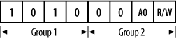
Connecting A0 directly to ground sets that address bit to 0 and therefore maps the PCF8583 to I2C address 0x50. Alternatively, if A0 is tied to VDD, then the address of the device is 0x51.
The schematic for interfacing the PCF8583 to a microcontroller is shown in Figure 8-9.
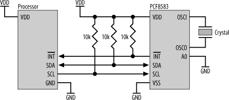
SDA and SCL both require pull-up resistors to VDD. The PCF8583 also has an internal alarm function and asserts an output (![]() ) for interrupting the processor. Since this output is open-drain, a pull-up resistor is also required.
) for interrupting the processor. Since this output is open-drain, a pull-up resistor is also required.
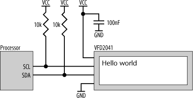
Adding a Small Display with I2C
You can use I2C to add simple LCDs (and other equivalent display technologies) to your embedded computer. These LCDs are usually just a few lines of text high, but are useful for simple message display functions. Matrix Orbital (http://www.matrixorbital.com) produces a number of display modules that are easy to interface, such as the VFD2041. This display module is 80 characters wide by 4 lines deep. The interface circuit is shown in Figure 8-10, and, as you can see, there’s almost nothing to it. The types of LCDs found in laptops are considerably more complicated, and interfacing them to small processors is just not an option. But for simple message displays (such as on the front panel of an appliance), a circuit like this is ideal.
Many Matrix Orbital displays also come with RS-232C interfaces, so if your embedded processor doesn’t support I2C, it’s still easy to add a small display.
[*] An open-drain or open-collector pin has output drivers that can only pull the signal line to ground. They cannot drive it high. This has the advantage that more than one device connected to a signal line may pull it low. If this were not the case, one device attempting to pull the line low while another tried to pull it high would result in a short circuit, with disastrous results. Interrupt lines are typically open-collector. All open-collector signals need a pull-up resistor and are active low. The idle state (when no device is asserting) is to be pulled high by the resistor.