
2
Combinational Logic Design
2.1 Introduction
In digital electronics, a circuit is a network that processes discrete-valued variables. A circuit can be viewed as a black box, shown in Figure 2.1, with
![]() one or more discrete-valued input terminals
one or more discrete-valued input terminals
![]() one or more discrete-valued output terminals
one or more discrete-valued output terminals
![]() a functional specification describing the relationship between inputs and outputs
a functional specification describing the relationship between inputs and outputs
![]() a timing specification describing the delay between inputs changing and outputs responding.
a timing specification describing the delay between inputs changing and outputs responding.
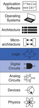
Figure 2.1 Circuit as a black box with inputs, outputs, and specifications
Peering inside the black box, circuits are composed of nodes and elements. An element is itself a circuit with inputs, outputs, and a specification. A node is a wire, whose voltage conveys a discrete-valued variable. Nodes are classified as input, output, or internal. Inputs receive values from the external world. Outputs deliver values to the external world. Wires that are not inputs or outputs are called internal nodes. Figure 2.2 illustrates a circuit with three elements, E1, E2, and E3, and six nodes. Nodes A, B, and C are inputs. Y and Z are outputs. n1 is an internal node between E1 and E3.

Figure 2.2 Elements and nodes
Digital circuits are classified as combinational or sequential. A combinational circuit’s outputs depend only on the current values of the inputs; in other words, it combines the current input values to compute the output. For example, a logic gate is a combinational circuit. A sequential circuit’s outputs depend on both current and previous values of the inputs; in other words, it depends on the input sequence. A combinational circuit is memoryless, but a sequential circuit has memory. This chapter focuses on combinational circuits, and Chapter 3 examines sequential circuits.
The functional specification of a combinational circuit expresses the output values in terms of the current input values. The timing specification of a combinational circuit consists of lower and upper bounds on the delay from input to output. We will initially concentrate on the functional specification, then return to the timing specification later in this chapter.
Figure 2.3 shows a combinational circuit with two inputs and one output. On the left of the figure are the inputs, A and B, and on the right is the output, Y. The symbol ![]() inside the box indicates that it is implemented using only combinational logic. In this example, the function F is specified to be OR: Y = F(A, B) = A + B. In words, we say the output Y is a function of the two inputs, A and B, namely Y = A OR B.
inside the box indicates that it is implemented using only combinational logic. In this example, the function F is specified to be OR: Y = F(A, B) = A + B. In words, we say the output Y is a function of the two inputs, A and B, namely Y = A OR B.

Figure 2.3 Combinational logic circuit
Figure 2.4 shows two possible implementations for the combinational logic circuit in Figure 2.3. As we will see repeatedly throughout the book, there are often many implementations for a single function. You choose which to use given the building blocks at your disposal and your design constraints. These constraints often include area, speed, power, and design time.
Figure 2.4 Two OR implementations
Figure 2.5 shows a combinational circuit with multiple outputs. This particular combinational circuit is called a full adder and we will revisit it in Section 5.2.1. The two equations specify the function of the outputs, S and Cout, in terms of the inputs, A, B, and Cin.
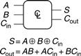
Figure 2.5 Multiple-output combinational circuit
To simplify drawings, we often use a single line with a slash through it and a number next to it to indicate a bus, a bundle of multiple signals. The number specifies how many signals are in the bus. For example, Figure 2.6(a) represents a block of combinational logic with three inputs and two outputs. If the number of bits is unimportant or obvious from the context, the slash may be shown without a number. Figure 2.6(b) indicates two blocks of combinational logic with an arbitrary number of outputs from one block serving as inputs to the second block.
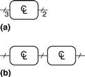
Figure 2.6 Slash notation for multiple signals
The rules of combinational composition tell us how we can build a large combinational circuit from smaller combinational circuit elements. A circuit is combinational if it consists of interconnected circuit elements such that
![]() Every circuit element is itself combinational.
Every circuit element is itself combinational.
![]() Every node of the circuit is either designated as an input to the circuit or connects to exactly one output terminal of a circuit element.
Every node of the circuit is either designated as an input to the circuit or connects to exactly one output terminal of a circuit element.
![]() The circuit contains no cyclic paths: every path through the circuit visits each circuit node at most once.
The circuit contains no cyclic paths: every path through the circuit visits each circuit node at most once.
Example 2.1 Combinational Circuits
Which of the circuits in Figure 2.7 are combinational circuits according to the rules of combinational composition?
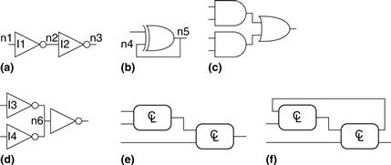
Figure 2.7 Example circuits
Solution
Circuit (a) is combinational. It is constructed from two combinational circuit elements (inverters I1 and I2). It has three nodes: n1, n2, and n3. n1 is an input to the circuit and to I1; n2 is an internal node, which is the output of I1 and the input to I2; n3 is the output of the circuit and of I2. (b) is not combinational, because there is a cyclic path: the output of the XOR feeds back to one of its inputs. Hence, a cyclic path starting at n4 passes through the XOR to n5, which returns to n4. (c) is combinational. (d) is not combinational, because node n6 connects to the output terminals of both I3 and I4. (e) is combinational, illustrating two combinational circuits connected to form a larger combinational circuit. (f) does not obey the rules of combinational composition because it has a cyclic path through the two elements. Depending on the functions of the elements, it may or may not be a combinational circuit.
Large circuits such as microprocessors can be very complicated, so we use the principles from Chapter 1 to manage the complexity. Viewing a circuit as a black box with a well-defined interface and function is an application of abstraction and modularity. Building the circuit out of smaller circuit elements is an application of hierarchy. The rules of combinational composition are an application of discipline.
The rules of combinational composition are sufficient but not strictly necessary. Certain circuits that disobey these rules are still combinational, so long as the outputs depend only on the current values of the inputs. However, determining whether oddball circuits are combinational is more difficult, so we will usually restrict ourselves to combinational composition as a way to build combinational circuits.
The functional specification of a combinational circuit is usually expressed as a truth table or a Boolean equation. In the next sections, we describe how to derive a Boolean equation from any truth table and how to use Boolean algebra and Karnaugh maps to simplify equations. We show how to implement these equations using logic gates and how to analyze the speed of these circuits.
2.2 Boolean Equations
Boolean equations deal with variables that are either TRUE or FALSE, so they are perfect for describing digital logic. This section defines some terminology commonly used in Boolean equations, then shows how to write a Boolean equation for any logic function given its truth table.
2.2.1 Terminology
The complement of a variable A is its inverse ![]() . The variable or its complement is called a literal. For example, A,
. The variable or its complement is called a literal. For example, A, ![]() , B, and
, B, and ![]() are literals. We call A the true form of the variable and
are literals. We call A the true form of the variable and ![]() the complementary form; “true form” does not mean that A is TRUE, but merely that A does not have a line over it.
the complementary form; “true form” does not mean that A is TRUE, but merely that A does not have a line over it.
The AND of one or more literals is called a product or an implicant. ![]() ,
, ![]() , and B are all implicants for a function of three variables. A minterm is a product involving all of the inputs to the function.
, and B are all implicants for a function of three variables. A minterm is a product involving all of the inputs to the function. ![]() is a minterm for a function of the three variables A, B, and C, but
is a minterm for a function of the three variables A, B, and C, but ![]() is not, because it does not involve C. Similarly, the OR of one or more literals is called a sum. A maxterm is a sum involving all of the inputs to the function. A +
is not, because it does not involve C. Similarly, the OR of one or more literals is called a sum. A maxterm is a sum involving all of the inputs to the function. A + ![]() + C is a maxterm for a function of the three variables A, B, and C.
+ C is a maxterm for a function of the three variables A, B, and C.
The order of operations is important when interpreting Boolean equations. Does Y = A + BC mean Y = (A OR B) AND C or Y = A OR (B AND C)? In Boolean equations, NOT has the highest precedence, followed by AND, then OR. Just as in ordinary equations, products are performed before sums. Therefore, the equation is read as Y = A OR (B AND C). Equation 2.1 gives another example of order of operations.
![]() (2.1)
(2.1)
2.2.2 Sum-of-Products Form
A truth table of N inputs contains 2N rows, one for each possible value of the inputs. Each row in a truth table is associated with a minterm that is TRUE for that row. Figure 2.8 shows a truth table of two inputs, A and B. Each row shows its corresponding minterm. For example, the minterm for the first row is ![]() because
because ![]() is TRUE when A = 0, B = 0. The minterms are numbered starting with 0; the top row corresponds to minterm 0, m0, the next row to minterm 1, m1, and so on.
is TRUE when A = 0, B = 0. The minterms are numbered starting with 0; the top row corresponds to minterm 0, m0, the next row to minterm 1, m1, and so on.
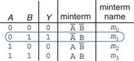
Figure 2.8 Truth table and minterms
We can write a Boolean equation for any truth table by summing each of the minterms for which the output, Y, is TRUE. For example, in Figure 2.8, there is only one row (or minterm) for which the output Y is TRUE, shown circled in blue. Thus, Y = ![]() . Figure 2.9 shows a truth table with more than one row in which the output is TRUE. Taking the sum of each of the circled minterms gives
. Figure 2.9 shows a truth table with more than one row in which the output is TRUE. Taking the sum of each of the circled minterms gives ![]()
Canonical form is just a fancy word for standard form. You can use the term to impress your friends and scare your enemies.
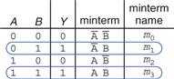
Figure 2.9 Truth table with multiple TRUE minterms
This is called the sum-of-products canonical form of a function because it is the sum (OR) of products (ANDs forming minterms). Although there are many ways to write the same function, such as ![]() we will sort the minterms in the same order that they appear in the truth table, so that we always write the same Boolean expression for the same truth table.
we will sort the minterms in the same order that they appear in the truth table, so that we always write the same Boolean expression for the same truth table.
The sum-of-products canonical form can also be written in sigma notation using the summation symbol, Σ. With this notation, the function from Figure 2.9 would be written as:
![]() (2.2)
(2.2)
or
![]()
Example 2.2 Sum-of-Products Form
Ben Bitdiddle is having a picnic. He won’t enjoy it if it rains or if there are ants. Design a circuit that will output TRUE only if Ben enjoys the picnic.
Solution
First define the inputs and outputs. The inputs are A and R, which indicate if there are ants and if it rains. A is TRUE when there are ants and FALSE when there are no ants. Likewise, R is TRUE when it rains and FALSE when the sun smiles on Ben. The output is E, Ben’s enjoyment of the picnic. E is TRUE if Ben enjoys the picnic and FALSE if he suffers. Figure 2.10 shows the truth table for Ben’s picnic experience.

Figure 2.10 Ben’s truth table
Using sum-of-products form, we write the equation as: ![]() or
or ![]() . We can build the equation using two inverters and a two-input AND gate, shown in Figure 2.11(a). You may recognize this truth table as the NOR function from Section 1.5.5: E = A NOR
. We can build the equation using two inverters and a two-input AND gate, shown in Figure 2.11(a). You may recognize this truth table as the NOR function from Section 1.5.5: E = A NOR ![]() Figure 2.11(b) shows the NOR implementation. In Section 2.3, we show that the two equations,
Figure 2.11(b) shows the NOR implementation. In Section 2.3, we show that the two equations, ![]() and
and ![]() , are equivalent.
, are equivalent.

Figure 2.11 Ben’s circuit

The sum-of-products form provides a Boolean equation for any truth table with any number of variables. Figure 2.12 shows a random three-input truth table. The sum-of-products form of the logic function is
![]() (2.3)
(2.3)
or
![]()
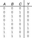
Figure 2.12 Random three-input truth table
Unfortunately, sum-of-products form does not necessarily generate the simplest equation. In Section 2.3 we show how to write the same function using fewer terms.
2.2.3 Product-of-Sums Form
An alternative way of expressing Boolean functions is the product-of-sums canonical form. Each row of a truth table corresponds to a maxterm that is FALSE for that row. For example, the maxterm for the first row of a two-input truth table is (A + B) because (A + B) is FALSE when A = 0, B = 0. We can write a Boolean equation for any circuit directly from the truth table as the AND of each of the maxterms for which the output is FALSE. The product-of-sums canonical form can also be written in pi notation using the product symbol, Π.
Example 2.3 Product-of-Sums Form
Write an equation in product-of-sums form for the truth table in Figure 2.13.
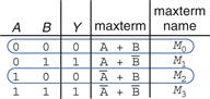
Figure 2.13 Truth table with multiple FALSE maxterms
Solution
The truth table has two rows in which the output is FALSE. Hence, the function can be written in product-of-sums form as ![]() or, using pi notation,
or, using pi notation, ![]() or
or ![]() . The first maxterm, (A + B), guarantees that Y = 0 for A = 0, B = 0, because any value AND 0 is 0. Likewise, the second maxterm,
. The first maxterm, (A + B), guarantees that Y = 0 for A = 0, B = 0, because any value AND 0 is 0. Likewise, the second maxterm, ![]() guarantees that Y = 0 for A = 1, B = 0. Figure 2.13 is the same truth table as Figure 2.9, showing that the same function can be written in more than one way.
guarantees that Y = 0 for A = 1, B = 0. Figure 2.13 is the same truth table as Figure 2.9, showing that the same function can be written in more than one way.
Similarly, a Boolean equation for Ben’s picnic from Figure 2.10 can be written in product-of-sums form by circling the three rows of 0’s to obtain ![]() or
or ![]() . This is uglier than the sum-of-products equation,
. This is uglier than the sum-of-products equation, ![]() , but the two equations are logically equivalent.
, but the two equations are logically equivalent.
Sum-of-products produces a shorter equation when the output is TRUE on only a few rows of a truth table; product-of-sums is simpler when the output is FALSE on only a few rows of a truth table.
2.3 Boolean Algebra
In the previous section, we learned how to write a Boolean expression given a truth table. However, that expression does not necessarily lead to the simplest set of logic gates. Just as you use algebra to simplify mathematical equations, you can use Boolean algebra to simplify Boolean equations. The rules of Boolean algebra are much like those of ordinary algebra but are in some cases simpler, because variables have only two possible values: 0 or 1.
Boolean algebra is based on a set of axioms that we assume are correct. Axioms are unprovable in the sense that a definition cannot be proved. From these axioms, we prove all the theorems of Boolean algebra. These theorems have great practical significance, because they teach us how to simplify logic to produce smaller and less costly circuits.
Axioms and theorems of Boolean algebra obey the principle of duality. If the symbols 0 and 1 and the operators • (AND) and + (OR) are interchanged, the statement will still be correct. We use the prime symbol (′) to denote the dual of a statement.
2.3.1 Axioms
Table 2.1 states the axioms of Boolean algebra. These five axioms and their duals define Boolean variables and the meanings of NOT, AND, and OR. Axiom A1 states that a Boolean variable B is 0 if it is not 1. The axiom’s dual, A1′, states that the variable is 1 if it is not 0. Together, A1 and A1′ tell us that we are working in a Boolean or binary field of 0’s and 1’s. Axioms A2 and A2′ define the NOT operation. Axioms A3 to A5 define AND; their duals, A3′ to A5′ define OR.
Table 2.1 Axioms of Boolean algebra

2.3.2 Theorems of One Variable
Theorems T1 to T5 in Table 2.2 describe how to simplify equations involving one variable.
Table 2.2 Boolean theorems of one variable
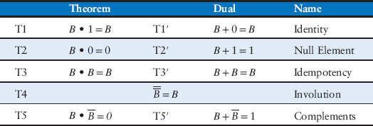
The identity theorem, T1, states that for any Boolean variable B, B AND 1 = B. Its dual states that B OR 0 = B. In hardware, as shown in Figure 2.14, T1 means that if one input of a two-input AND gate is always 1, we can remove the AND gate and replace it with a wire connected to the variable input (B). Likewise, T1′ means that if one input of a two-input OR gate is always 0, we can replace the OR gate with a wire connected to B. In general, gates cost money, power, and delay, so replacing a gate with a wire is beneficial.
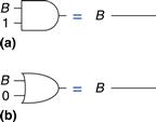
Figure 2.14 Identity theorem in hardware: (a) T1, (b) T1′
The null element theorem, T2, says that B AND 0 is always equal to 0. Therefore, 0 is called the null element for the AND operation, because it nullifies the effect of any other input. The dual states that B OR 1 is always equal to 1. Hence, 1 is the null element for the OR operation. In hardware, as shown in Figure 2.15, if one input of an AND gate is 0, we can replace the AND gate with a wire that is tied LOW (to 0). Likewise, if one input of an OR gate is 1, we can replace the OR gate with a wire that is tied HIGH (to 1).
The null element theorem leads to some outlandish statements that are actually true! It is particularly dangerous when left in the hands of advertisers: YOU WILL GET A MILLION DOLLARS or we’ll send you a toothbrush in the mail. (You’ll most likely be receiving a toothbrush in the mail.)
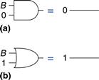
Figure 2.15 Null element theorem in hardware: (a) T2, (b) T2′
Idempotency, T3, says that a variable AND itself is equal to just itself. Likewise, a variable OR itself is equal to itself. The theorem gets its name from the Latin roots: idem (same) and potent (power). The operations return the same thing you put into them. Figure 2.16 shows that idempotency again permits replacing a gate with a wire.
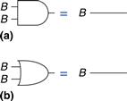
Figure 2.16 Idempotency theorem in hardware: (a) T3, (b) T3′
Involution, T4, is a fancy way of saying that complementing a variable twice results in the original variable. In digital electronics, two wrongs make a right. Two inverters in series logically cancel each other out and are logically equivalent to a wire, as shown in Figure 2.17. The dual of T4 is itself.
![]()
Figure 2.17 Involution theorem in hardware: T4
The complement theorem, T5 (Figure 2.18), states that a variable AND its complement is 0 (because one of them has to be 0). And by duality, a variable OR its complement is 1 (because one of them has to be 1).
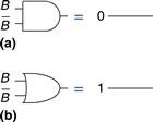
Figure 2.18 Complement theorem in hardware: (a) T5, (b) T5′
2.3.3 Theorems of Several Variables
Theorems T6 to T12 in Table 2.3 describe how to simplify equations involving more than one Boolean variable.
Table 2.3 Boolean theorems of several variables
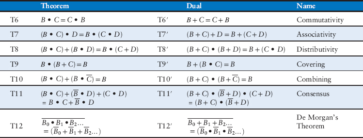
Commutativity and associativity, T6 and T7, work the same as in traditional algebra. By commutativity, the order of inputs for an AND or OR function does not affect the value of the output. By associativity, the specific groupings of inputs do not affect the value of the output.
The distributivity theorem, T8, is the same as in traditional algebra, but its dual, T8′, is not. By T8, AND distributes over OR, and by T8′, OR distributes over AND. In traditional algebra, multiplication distributes over addition but addition does not distribute over multiplication, so that (B + C) × (B + D) ≠ B + (C × D).
The covering, combining, and consensus theorems, T9 to T11, permit us to eliminate redundant variables. With some thought, you should be able to convince yourself that these theorems are correct.
De Morgan’s Theorem, T12, is a particularly powerful tool in digital design. The theorem explains that the complement of the product of all the terms is equal to the sum of the complement of each term. Likewise, the complement of the sum of all the terms is equal to the product of the complement of each term.
According to De Morgan’s theorem, a NAND gate is equivalent to an OR gate with inverted inputs. Similarly, a NOR gate is equivalent to an AND gate with inverted inputs. Figure 2.19 shows these De Morgan equivalent gates for NAND and NOR gates. The two symbols shown for each function are called duals. They are logically equivalent and can be used interchangeably.
Augustus De Morgan, died 1871
A British mathematician, born in India. Blind in one eye. His father died when he was 10. Attended Trinity College, Cambridge, at age 16, and was appointed Professor of Mathematics at the newly founded London University at age 22. Wrote widely on many mathematical subjects, including logic, algebra, and paradoxes. De Morgan’s crater on the moon is named for him. He proposed a riddle for the year of his birth: “I was x years of age in the year x2.”
Figure 2.19 De Morgan equivalent gates
The inversion circle is called a bubble. Intuitively, you can imagine that “pushing” a bubble through the gate causes it to come out at the other side and flips the body of the gate from AND to OR or vice versa. For example, the NAND gate in Figure 2.19 consists of an AND body with a bubble on the output. Pushing the bubble to the left results in an OR body with bubbles on the inputs. The underlying rules for bubble pushing are
• Pushing bubbles backward (from the output) or forward (from the inputs) changes the body of the gate from AND to OR or vice versa.
• Pushing a bubble from the output back to the inputs puts bubbles on all gate inputs.
• Pushing bubbles on all gate inputs forward toward the output puts a bubble on the output.
Section 2.5.2 uses bubble pushing to help analyze circuits.
Example 2.4 Derive the Product-of-Sums Form
Figure 2.20 shows the truth table for a Boolean function Y and its complement ![]() Using De Morgan’s Theorem, derive the product-of-sums canonical form of Y from the sum-of-products form of
Using De Morgan’s Theorem, derive the product-of-sums canonical form of Y from the sum-of-products form of ![]()
Figure 2.20 Truth table showing Y and ![]()
Solution
Figure 2.21 shows the minterms (circled) contained in ![]() The sum-of-products canonical form of
The sum-of-products canonical form of ![]() is
is
![]() (2.4)
(2.4)
Figure 2.21 Truth table showing minterms for ![]()
Taking the complement of both sides and applying De Morgan’s Theorem twice, we get:
![]() (2.5)
(2.5)
2.3.4 The Truth Behind It All
The curious reader might wonder how to prove that a theorem is true. In Boolean algebra, proofs of theorems with a finite number of variables are easy: just show that the theorem holds for all possible values of these variables. This method is called perfect induction and can be done with a truth table.
Example 2.5 Proving the Consensus Theorem Using Perfect Induction
Prove the consensus theorem, T11, from Table 2.3.
Solution
Check both sides of the equation for all eight combinations of B, C, and D. The truth table in Figure 2.22 illustrates these combinations. Because ![]() for all cases, the theorem is proved.
for all cases, the theorem is proved.
Figure 2.22 Truth table proving T11
2.3.5 Simplifying Equations
The theorems of Boolean algebra help us simplify Boolean equations. For example, consider the sum-of-products expression from the truth table of Figure 2.9: ![]() By Theorem T10, the equation simplifies to
By Theorem T10, the equation simplifies to ![]() This may have been obvious looking at the truth table. In general, multiple steps may be necessary to simplify more complex equations.
This may have been obvious looking at the truth table. In general, multiple steps may be necessary to simplify more complex equations.
The basic principle of simplifying sum-of-products equations is to combine terms using the relationship ![]() where P may be any implicant. How far can an equation be simplified? We define an equation in sum-of-products form to be minimized if it uses the fewest possible implicants. If there are several equations with the same number of implicants, the minimal one is the one with the fewest literals.
where P may be any implicant. How far can an equation be simplified? We define an equation in sum-of-products form to be minimized if it uses the fewest possible implicants. If there are several equations with the same number of implicants, the minimal one is the one with the fewest literals.
An implicant is called a prime implicant if it cannot be combined with any other implicants in the equation to form a new implicant with fewer literals. The implicants in a minimal equation must all be prime implicants. Otherwise, they could be combined to reduce the number of literals.
Example 2.6 Equation Minimization
Minimize Equation 2.3: ![]()
Solution
We start with the original equation and apply Boolean theorems step by step, as shown in Table 2.4.
Table 2.4 Equation minimization
Have we simplified the equation completely at this point? Let’s take a closer look. From the original equation, the minterms ![]() and
and ![]() differ only in the variable A. So we combined the minterms to form
differ only in the variable A. So we combined the minterms to form ![]() However, if we look at the original equation, we note that the last two minterms
However, if we look at the original equation, we note that the last two minterms ![]() and
and ![]() also differ by a single literal (C and
also differ by a single literal (C and ![]() ). Thus, using the same method, we could have combined these two minterms to form the minterm
). Thus, using the same method, we could have combined these two minterms to form the minterm ![]() We say that implicants
We say that implicants ![]() and
and ![]() share the minterm
share the minterm ![]()
So, are we stuck with simplifying only one of the minterm pairs, or can we simplify both? Using the idempotency theorem, we can duplicate terms as many times as we want: B = B + B + B + B … . Using this principle, we simplify the equation completely to its two prime implicants, ![]() as shown in Table 2.5.
as shown in Table 2.5.
Table 2.5 Improved equation minimization
Although it is a bit counterintuitive, expanding an implicant (for example, turning AB into ABC + ![]() ) is sometimes useful in minimizing equations. By doing this, you can repeat one of the expanded minterms to be combined (shared) with another minterm.
) is sometimes useful in minimizing equations. By doing this, you can repeat one of the expanded minterms to be combined (shared) with another minterm.
You may have noticed that completely simplifying a Boolean equation with the theorems of Boolean algebra can take some trial and error. Section 2.7 describes a methodical technique called Karnaugh maps that makes the process easier.
Why bother simplifying a Boolean equation if it remains logically equivalent? Simplifying reduces the number of gates used to physically implement the function, thus making it smaller, cheaper, and possibly faster. The next section describes how to implement Boolean equations with logic gates.
2.4 From Logic to Gates
A schematic is a diagram of a digital circuit showing the elements and the wires that connect them together. For example, the schematic in Figure 2.23 shows a possible hardware implementation of our favorite logic function, Equation 2.3:
![]()

Figure 2.23 Schematic of ![]()
By drawing schematics in a consistent fashion, we make them easier to read and debug. We will generally obey the following guidelines:
![]() Inputs are on the left (or top) side of a schematic.
Inputs are on the left (or top) side of a schematic.
![]() Outputs are on the right (or bottom) side of a schematic.
Outputs are on the right (or bottom) side of a schematic.
![]() Whenever possible, gates should flow from left to right.
Whenever possible, gates should flow from left to right.
![]() Straight wires are better to use than wires with multiple corners (jagged wires waste mental effort following the wire rather than thinking of what the circuit does).
Straight wires are better to use than wires with multiple corners (jagged wires waste mental effort following the wire rather than thinking of what the circuit does).
![]() Wires always connect at a T junction.
Wires always connect at a T junction.
![]() A dot where wires cross indicates a connection between the wires.
A dot where wires cross indicates a connection between the wires.
The last three guidelines are illustrated in Figure 2.24.
Figure 2.24 Wire connections
Any Boolean equation in sum-of-products form can be drawn as a schematic in a systematic way similar to Figure 2.23. First, draw columns for the inputs. Place inverters in adjacent columns to provide the complementary inputs if necessary. Draw rows of AND gates for each of the minterms. Then, for each output, draw an OR gate connected to the minterms related to that output. This style is called a programmable logic array (PLA) because the inverters, AND gates, and OR gates are arrayed in a systematic fashion. PLAs will be discussed further in Section 5.6.
Figure 2.25 shows an implementation of the simplified equation we found using Boolean algebra in Example 2.6. Notice that the simplified circuit has significantly less hardware than that of Figure 2.23. It may also be faster, because it uses gates with fewer inputs.
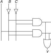
Figure 2.25 Schematic of ![]()
We can reduce the number of gates even further (albeit by a single inverter) by taking advantage of inverting gates. Observe that ![]() is an AND with inverted inputs. Figure 2.26 shows a schematic using this optimization to eliminate the inverter on C. Recall that by De Morgan’s theorem the AND with inverted inputs is equivalent to a NOR gate. Depending on the implementation technology, it may be cheaper to use the fewest gates or to use certain types of gates in preference to others. For example, NANDs and NORs are preferred over ANDs and ORs in CMOS implementations.
is an AND with inverted inputs. Figure 2.26 shows a schematic using this optimization to eliminate the inverter on C. Recall that by De Morgan’s theorem the AND with inverted inputs is equivalent to a NOR gate. Depending on the implementation technology, it may be cheaper to use the fewest gates or to use certain types of gates in preference to others. For example, NANDs and NORs are preferred over ANDs and ORs in CMOS implementations.
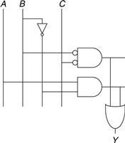
Figure 2.26 Schematic using fewer gates
Many circuits have multiple outputs, each of which computes a separate Boolean function of the inputs. We can write a separate truth table for each output, but it is often convenient to write all of the outputs on a single truth table and sketch one schematic with all of the outputs.
Example 2.7 Multiple-Output Circuits
The dean, the department chair, the teaching assistant, and the dorm social chair each use the auditorium from time to time. Unfortunately, they occasionally conflict, leading to disasters such as the one that occurred when the dean’s fundraising meeting with crusty trustees happened at the same time as the dorm’s BTB1 party. Alyssa P. Hacker has been called in to design a room reservation system.
The system has four inputs, A3, … , A0, and four outputs, Y3, … , Y0. These signals can also be written as A3:0 and Y3:0. Each user asserts her input when she requests the auditorium for the next day. The system asserts at most one output, granting the auditorium to the highest priority user. The dean, who is paying for the system, demands highest priority (3). The department chair, teaching assistant, and dorm social chair have decreasing priority.
Write a truth table and Boolean equations for the system. Sketch a circuit that performs this function.
Solution
This function is called a four-input priority circuit. Its symbol and truth table are shown in Figure 2.27.
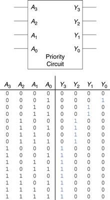
Figure 2.27 Priority circuit
We could write each output in sum-of-products form and reduce the equations using Boolean algebra. However, the simplified equations are clear by inspection from the functional description (and the truth table): Y3 is TRUE whenever A3 is asserted, so Y3 = Α3. Y2 is TRUE if A2 is asserted and A3 is not asserted, so ![]() is TRUE if A1 is asserted and neither of the higher priority inputs is asserted:
is TRUE if A1 is asserted and neither of the higher priority inputs is asserted: ![]() And Y0 is TRUE whenever A0 and no other input is asserted:
And Y0 is TRUE whenever A0 and no other input is asserted: ![]() The schematic is shown in Figure 2.28. An experienced designer can often implement a logic circuit by inspection. Given a clear specification, simply turn the words into equations and the equations into gates.
The schematic is shown in Figure 2.28. An experienced designer can often implement a logic circuit by inspection. Given a clear specification, simply turn the words into equations and the equations into gates.

Figure 2.28 Priority circuit schematic
Notice that if A3 is asserted in the priority circuit, the outputs don’t care what the other inputs are. We use the symbol X to describe inputs that the output doesn’t care about. Figure 2.29 shows that the four-input priority circuit truth table becomes much smaller with don’t cares. From this truth table, we can easily read the Boolean equations in sum-of-products form by ignoring inputs with X’s. Don’t cares can also appear in truth table outputs, as we will see in Section 2.7.3.
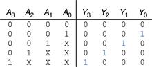
Figure 2.29 Priority circuit truth table with don’t cares (X’s)
2.5 Multilevel Combinational Logic
Logic in sum-of-products form is called two-level logic because it consists of literals connected to a level of AND gates connected to a level of OR gates. Designers often build circuits with more than two levels of logic gates. These multilevel combinational circuits may use less hardware than their two-level counterparts. Bubble pushing is especially helpful in analyzing and designing multilevel circuits.
X is an overloaded symbol that means “don’t care” in truth tables and “contention” in logic simulation (see Section 2.6.1). Think about the context so you don’t mix up the meanings. Some authors use D or ? instead for “don’t care” to avoid this ambiguity.
2.5.1 Hardware Reduction
Some logic functions require an enormous amount of hardware when built using two-level logic. A notable example is the XOR function of multiple variables. For example, consider building a three-input XOR using the two-level techniques we have studied so far.
Recall that an N-input XOR produces a TRUE output when an odd number of inputs are TRUE. Figure 2.30 shows the truth table for a three-input XOR with the rows circled that produce TRUE outputs. From the truth table, we read off a Boolean equation in sum-of-products form in Equation 2.6. Unfortunately, there is no way to simplify this equation into fewer implicants.
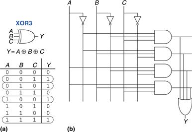
Figure 2.30 Three-input XOR: (a) functional specification and (b) two-level logic implementation
![]() (2.6)
(2.6)
On the other hand, A ⊕ B ⊕ C = (A ⊕ B) ⊕ C (prove this to yourself by perfect induction if you are in doubt). Therefore, the three-input XOR can be built out of a cascade of two-input XORs, as shown in Figure 2.31.
![]()
Figure 2.31 Three-input XOR using two-input XORs
Similarly, an eight-input XOR would require 128 eight-input AND gates and one 128-input OR gate for a two-level sum-of-products implementation. A much better option is to use a tree of two-input XOR gates, as shown in Figure 2.32.

Figure 2.32 Eight-input XOR using seven two-input XORs
Selecting the best multilevel implementation of a specific logic function is not a simple process. Moreover, “best” has many meanings: fewest gates, fastest, shortest design time, least cost, least power consumption. In Chapter 5, you will see that the “best” circuit in one technology is not necessarily the best in another. For example, we have been using ANDs and ORs, but in CMOS, NANDs and NORs are more efficient. With some experience, you will find that you can create a good multilevel design by inspection for most circuits. You will develop some of this experience as you study circuit examples through the rest of this book. As you are learning, explore various design options and think about the trade-offs. Computer-aided design (CAD) tools are also available to search a vast space of possible multilevel designs and seek the one that best fits your constraints given the available building blocks.
2.5.2 Bubble Pushing
You may recall from Section 1.7.6 that CMOS circuits prefer NANDs and NORs over ANDs and ORs. But reading the equation by inspection from a multilevel circuit with NANDs and NORs can get pretty hairy. Figure 2.33 shows a multilevel circuit whose function is not immediately clear by inspection. Bubble pushing is a helpful way to redraw these circuits so that the bubbles cancel out and the function can be more easily determined. Building on the principles from Section 2.3.3, the guidelines for bubble pushing are as follows:
![]() Begin at the output of the circuit and work toward the inputs.
Begin at the output of the circuit and work toward the inputs.
![]() Push any bubbles on the final output back toward the inputs so that you can read an equation in terms of the output (for example, Y) instead of the complement of the output
Push any bubbles on the final output back toward the inputs so that you can read an equation in terms of the output (for example, Y) instead of the complement of the output ![]() .
.
![]() Working backward, draw each gate in a form so that bubbles cancel. If the current gate has an input bubble, draw the preceding gate with an output bubble. If the current gate does not have an input bubble, draw the preceding gate without an output bubble.
Working backward, draw each gate in a form so that bubbles cancel. If the current gate has an input bubble, draw the preceding gate with an output bubble. If the current gate does not have an input bubble, draw the preceding gate without an output bubble.
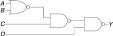
Figure 2.33 Multilevel circuit using NANDs and NORs
Figure 2.34 shows how to redraw Figure 2.33 according to the bubble pushing guidelines. Starting at the output Y, the NAND gate has a bubble on the output that we wish to eliminate. We push the output bubble back to form an OR with inverted inputs, shown in Figure 2.34(a). Working to the left, the rightmost gate has an input bubble that cancels with the output bubble of the middle NAND gate, so no change is necessary, as shown in Figure 2.34(b). The middle gate has no input bubble, so we transform the leftmost gate to have no output bubble, as shown in Figure 2.34(c). Now all of the bubbles in the circuit cancel except at the inputs, so the function can be read by inspection in terms of ANDs and ORs of true or complementary inputs: ![]()
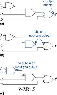
Figure 2.34 Bubble-pushed circuit
For emphasis of this last point, Figure 2.35 shows a circuit logically equivalent to the one in Figure 2.34. The functions of internal nodes are labeled in blue. Because bubbles in series cancel, we can ignore the bubbles on the output of the middle gate and on one input of the rightmost gate to produce the logically equivalent circuit of Figure 2.35.
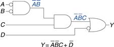
Figure 2.35 Logically equivalent bubble-pushed circuit
Example 2.8 Bubble Pushing for Cmos Logic
Most designers think in terms of AND and OR gates, but suppose you would like to implement the circuit in Figure 2.36 in CMOS logic, which favors NAND and NOR gates. Use bubble pushing to convert the circuit to NANDs, NORs, and inverters.
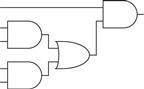
Figure 2.36 Circuit using ANDs and ORs
Solution
A brute force solution is to just replace each AND gate with a NAND and an inverter, and each OR gate with a NOR and an inverter, as shown in Figure 2.37. This requires eight gates. Notice that the inverter is drawn with the bubble on the front rather than back, to emphasize how the bubble can cancel with the preceding inverting gate.
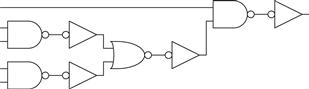
Figure 2.37 Poor circuit using NANDs and NORs
For a better solution, observe that bubbles can be added to the output of a gate and the input of the next gate without changing the function, as shown in Figure 2.38(a). The final AND is converted to a NAND and an inverter, as shown in Figure 2.38(b). This solution requires only five gates.
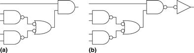
Figure 2.38 Better circuit using NANDs and NORs
2.6 X’s and Z’s, Oh My
Boolean algebra is limited to 0’s and 1’s. However, real circuits can also have illegal and floating values, represented symbolically by X and Z.
2.6.1 Illegal Value: X
The symbol X indicates that the circuit node has an unknown or illegal value. This commonly happens if it is being driven to both 0 and 1 at the same time. Figure 2.39 shows a case where node Y is driven both HIGH and LOW. This situation, called contention, is considered to be an error and must be avoided. The actual voltage on a node with contention may be somewhere between 0 and VDD, depending on the relative strengths of the gates driving HIGH and LOW. It is often, but not always, in the forbidden zone. Contention also can cause large amounts of power to flow between the fighting gates, resulting in the circuit getting hot and possibly damaged.
Figure 2.39 Circuit with contention
X values are also sometimes used by circuit simulators to indicate an uninitialized value. For example, if you forget to specify the value of an input, the simulator may assume it is an X to warn you of the problem.
As mentioned in Section 2.4, digital designers also use the symbol X to indicate “don’t care” values in truth tables. Be sure not to mix up the two meanings. When X appears in a truth table, it indicates that the value of the variable in the truth table is unimportant (can be either 0 or 1). When X appears in a circuit, it means that the circuit node has an unknown or illegal value.
2.6.2 Floating Value: Z
The symbol Z indicates that a node is being driven neither HIGH nor LOW. The node is said to be floating, high impedance, or high Z. A typical misconception is that a floating or undriven node is the same as a logic 0. In reality, a floating node might be 0, might be 1, or might be at some voltage in between, depending on the history of the system. A floating node does not always mean there is an error in the circuit, so long as some other circuit element does drive the node to a valid logic level when the value of the node is relevant to circuit operation.
One common way to produce a floating node is to forget to connect a voltage to a circuit input, or to assume that an unconnected input is the same as an input with the value of 0. This mistake may cause the circuit to behave erratically as the floating input randomly changes from 0 to 1. Indeed, touching the circuit may be enough to trigger the change by means of static electricity from the body. We have seen circuits that operate correctly only as long as the student keeps a finger pressed on a chip.
The tristate buffer, shown in Figure 2.40, has three possible output states: HIGH (1), LOW (0), and floating (Z). The tristate buffer has an input A, output Y, and enable E. When the enable is TRUE, the tristate buffer acts as a simple buffer, transferring the input value to the output. When the enable is FALSE, the output is allowed to float (Z).
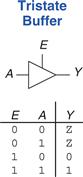
Figure 2.40 Tristate buffer
The tristate buffer in Figure 2.40 has an active high enable. That is, when the enable is HIGH (1), the buffer is enabled. Figure 2.41 shows a tristate buffer with an active low enable. When the enable is LOW (0), the buffer is enabled. We show that the signal is active low by putting a bubble on its input wire. We often indicate an active low input by drawing a bar over its name, ![]() , or appending the letters “b” or “bar” after its name, Eb or Ebar.
, or appending the letters “b” or “bar” after its name, Eb or Ebar.
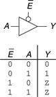
Figure 2.41 Tristate buffer with active low enable
Tristate buffers are commonly used on busses that connect multiple chips. For example, a microprocessor, a video controller, and an Ethernet controller might all need to communicate with the memory system in a personal computer. Each chip can connect to a shared memory bus using tristate buffers, as shown in Figure 2.42. Only one chip at a time is allowed to assert its enable signal to drive a value onto the bus. The other chips must produce floating outputs so that they do not cause contention with the chip talking to the memory. Any chip can read the information from the shared bus at any time. Such tristate busses were once common. However, in modern computers, higher speeds are possible with point-to-point links, in which chips are connected to each other directly rather than over a shared bus.

Figure 2.42 Tristate bus connecting multiple chips
2.7 Karnaugh Maps
After working through several minimizations of Boolean equations using Boolean algebra, you will realize that, if you’re not careful, you sometimes end up with a completely different equation instead of a simplified equation. Karnaugh maps (K-maps) are a graphical method for simplifying Boolean equations. They were invented in 1953 by Maurice Karnaugh, a telecommunications engineer at Bell Labs. K-maps work well for problems with up to four variables. More important, they give insight into manipulating Boolean equations.
Maurice Karnaugh, 1924–. Graduated with a bachelor’s degree in physics from the City College of New York in 1948 and earned a Ph.D. in physics from Yale in 1952.
Worked at Bell Labs and IBM from 1952 to 1993 and as a computer science professor at the Polytechnic University of New York from 1980 to 1999.
Gray codes were patented (U.S. Patent 2,632,058) by Frank Gray, a Bell Labs researcher, in 1953. They are especially useful in mechanical encoders because a slight misalignment causes an error in only one bit.
Gray codes generalize to any number of bits. For example, a 3-bit Gray code sequence is:
000, 001, 011, 010,
110, 111, 101, 100
Lewis Carroll posed a related puzzle in Vanity Fair in 1879.
“The rules of the Puzzle are simple enough. Two words are proposed, of the same length; and the puzzle consists of linking these together by interposing other words, each of which shall differ from the next word in one letter only. That is to say, one letter may be changed in one of the given words, then one letter in the word so obtained, and so on, till we arrive at the other given word.”
For example, SHIP to DOCK:
SHIP, SLIP, SLOP,
SLOT, SOOT, LOOT,
LOOK, LOCK, DOCK.
Can you find a shorter sequence?
Recall that logic minimization involves combining terms. Two terms containing an implicant P and the true and complementary forms of some variable A are combined to eliminate ![]() Karnaugh maps make these combinable terms easy to see by putting them next to each other in a grid.
Karnaugh maps make these combinable terms easy to see by putting them next to each other in a grid.
Figure 2.43 shows the truth table and K-map for a three-input function. The top row of the K-map gives the four possible values for the A and B inputs. The left column gives the two possible values for the C input. Each square in the K-map corresponds to a row in the truth table and contains the value of the output Y for that row. For example, the top left square corresponds to the first row in the truth table and indicates that the output value Y = 1 when ABC = 000. Just like each row in a truth table, each square in a K-map represents a single minterm. For the purpose of explanation, Figure 2.43(c) shows the minterm corresponding to each square in the K-map.
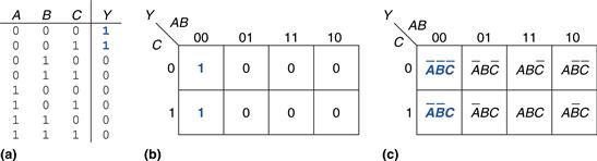
Figure 2.43 Three-input function: (a) truth table, (b) K-map, (c) K-map showing minterms
Each square, or minterm, differs from an adjacent square by a change in a single variable. This means that adjacent squares share all the same literals except one, which appears in true form in one square and in complementary form in the other. For example, the squares representing the minterms ![]() and
and ![]() are adjacent and differ only in the variable C. You may have noticed that the A and B combinations in the top row are in a peculiar order: 00, 01, 11, 10. This order is called a Gray code. It differs from ordinary binary order (00, 01, 10, 11) in that adjacent entries differ only in a single variable. For example, 01 : 11 only changes A from 0 to 1, while 01 : 10 would change A from 1 to 0 and B from 0 to 1. Hence, writing the combinations in binary order would not have produced our desired property of adjacent squares differing only in one variable.
are adjacent and differ only in the variable C. You may have noticed that the A and B combinations in the top row are in a peculiar order: 00, 01, 11, 10. This order is called a Gray code. It differs from ordinary binary order (00, 01, 10, 11) in that adjacent entries differ only in a single variable. For example, 01 : 11 only changes A from 0 to 1, while 01 : 10 would change A from 1 to 0 and B from 0 to 1. Hence, writing the combinations in binary order would not have produced our desired property of adjacent squares differing only in one variable.
The K-map also “wraps around.” The squares on the far right are effectively adjacent to the squares on the far left, in that they differ only in one variable, A. In other words, you could take the map and roll it into a cylinder, then join the ends of the cylinder to form a torus (i.e., a donut), and still guarantee that adjacent squares would differ only in one variable.
2.7.1 Circular Thinking
In the K-map in Figure 2.43, only two minterms are present in the equation, ![]() and
and ![]() as indicated by the 1’s in the left column. Reading the minterms from the K-map is exactly equivalent to reading equations in sum-of-products form directly from the truth table.
as indicated by the 1’s in the left column. Reading the minterms from the K-map is exactly equivalent to reading equations in sum-of-products form directly from the truth table.
As before, we can use Boolean algebra to minimize equations in sum-of-products form.
![]() (2.7)
(2.7)
K-maps help us do this simplification graphically by circling 1’s in adjacent squares, as shown in Figure 2.44. For each circle, we write the corresponding implicant. Remember from Section 2.2 that an implicant is the product of one or more literals. Variables whose true and complementary forms are both in the circle are excluded from the implicant. In this case, the variable C has both its true form (1) and its complementary form (0) in the circle, so we do not include it in the implicant. In other words, Y is TRUE when A = B = 0, independent of C. So the implicant is ![]() The K-map gives the same answer we reached using Boolean algebra.
The K-map gives the same answer we reached using Boolean algebra.
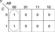
Figure 2.44 K-map minimization
2.7.2 Logic Minimization with K-Maps
K-maps provide an easy visual way to minimize logic. Simply circle all the rectangular blocks of 1’s in the map, using the fewest possible number of circles. Each circle should be as large as possible. Then read off the implicants that were circled.
More formally, recall that a Boolean equation is minimized when it is written as a sum of the fewest number of prime implicants. Each circle on the K-map represents an implicant. The largest possible circles are prime implicants.
For example, in the K-map of Figure 2.44, ![]() and
and ![]() are implicants, but not prime implicants. Only
are implicants, but not prime implicants. Only ![]() is a prime implicant in that K-map. Rules for finding a minimized equation from a K-map are as follows:
is a prime implicant in that K-map. Rules for finding a minimized equation from a K-map are as follows:
![]() Use the fewest circles necessary to cover all the 1’s.
Use the fewest circles necessary to cover all the 1’s.
![]() All the squares in each circle must contain 1’s.
All the squares in each circle must contain 1’s.
![]() Each circle must span a rectangular block that is a power of 2 (i.e., 1, 2, or 4) squares in each direction.
Each circle must span a rectangular block that is a power of 2 (i.e., 1, 2, or 4) squares in each direction.
![]() Each circle should be as large as possible.
Each circle should be as large as possible.
![]() A circle may wrap around the edges of the K-map.
A circle may wrap around the edges of the K-map.
![]() A 1 in a K-map may be circled multiple times if doing so allows fewer circles to be used.
A 1 in a K-map may be circled multiple times if doing so allows fewer circles to be used.
Example 2.9 Minimization of a Three-Variable Function Using a K-Map
Suppose we have the function Y = F(A, B, C) with the K-map shown in Figure 2.45. Minimize the equation using the K-map.

Figure 2.45 K-map for Example 2.9
Solution
Circle the 1’s in the K-map using as few circles as possible, as shown in Figure 2.46. Each circle in the K-map represents a prime implicant, and the dimension of each circle is a power of two (2 × 1 and 2 × 2). We form the prime implicant for each circle by writing those variables that appear in the circle only in true or only in complementary form.
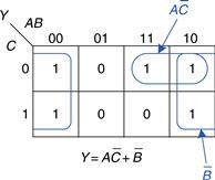
Figure 2.46 Solution for Example 2.9
For example, in the 2 × 1 circle, the true and complementary forms of B are included in the circle, so we do not include B in the prime implicant. However, only the true form of A (A) and complementary form of ![]() are in this circle, so we include these variables in the prime implicant
are in this circle, so we include these variables in the prime implicant ![]() Similarly, the 2 × 2 circle covers all squares where B = 0, so the prime implicant is
Similarly, the 2 × 2 circle covers all squares where B = 0, so the prime implicant is ![]()
Notice how the top-right square (minterm) is covered twice to make the prime implicant circles as large as possible. As we saw with Boolean algebra techniques, this is equivalent to sharing a minterm to reduce the size of the implicant. Also notice how the circle covering four squares wraps around the sides of the K-map.
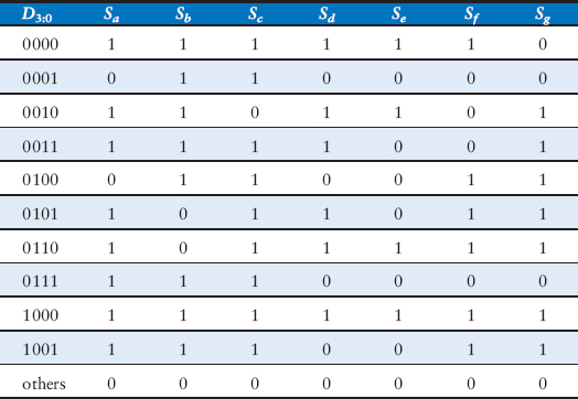
Example 2.10 Seven-Segment Display Decoder
A seven-segment display decoder takes a 4-bit data input D3:0 and produces seven outputs to control light-emitting diodes to display a digit from 0 to 9. The seven outputs are often called segments a through g, or Sa–Sg, as defined in Figure 2.47. The digits are shown in Figure 2.48. Write a truth table for the outputs, and use K-maps to find Boolean equations for outputs Sa and Sb. Assume that illegal input values (10–15) produce a blank readout.
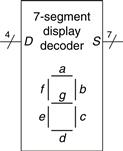
Figure 2.47 Seven-segment display decoder icon

Figure 2.48 Seven-segment display digits
Solution
The truth table is given in Table 2.6. For example, an input of 0000 should turn on all segments except Sg.
Table 2.6 Seven-segment display decoder truth table
Each of the seven outputs is an independent function of four variables. The K-maps for outputs Sa and Sb are shown in Figure 2.49. Remember that adjacent squares may differ in only a single variable, so we label the rows and columns in Gray code order: 00, 01, 11, 10. Be careful to also remember this ordering when entering the output values into the squares.

Figure 2.49 Karnaugh maps for Sa and Sb
Next, circle the prime implicants. Use the fewest number of circles necessary to cover all the 1’s. A circle can wrap around the edges (vertical and horizontal), and a 1 may be circled more than once. Figure 2.50 shows the prime implicants and the simplified Boolean equations.
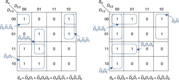
Figure 2.50 K-map solution for Example 2.10
Note that the minimal set of prime implicants is not unique. For example, the 0000 entry in the Sa K-map was circled along with the 1000 entry to produce the ![]() minterm. The circle could have included the 0010 entry instead, producing a
minterm. The circle could have included the 0010 entry instead, producing a ![]() minterm, as shown with dashed lines in Figure 2.51.
minterm, as shown with dashed lines in Figure 2.51.
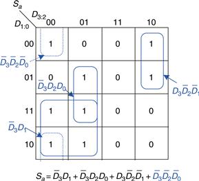
Figure 2.51 Alternative K-map for Sa showing different set of prime implicants
Figure 2.52 (see page 82) illustrates a common error in which a nonprime implicant was chosen to cover the 1 in the upper left corner. This minterm, ![]() gives a sum-of-products equation that is not minimal. The minterm could have been combined with either of the adjacent ones to form a larger circle, as was done in the previous two figures.
gives a sum-of-products equation that is not minimal. The minterm could have been combined with either of the adjacent ones to form a larger circle, as was done in the previous two figures.

Figure 2.52 Alternative K-map for Sa showing incorrect nonprime implicant
2.7.3 Don’t Cares
Recall that “don’t care” entries for truth table inputs were introduced in Section 2.4 to reduce the number of rows in the table when some variables do not affect the output. They are indicated by the symbol X, which means that the entry can be either 0 or 1.
Don’t cares also appear in truth table outputs where the output value is unimportant or the corresponding input combination can never happen. Such outputs can be treated as either 0’s or 1’s at the designer’s discretion.
In a K-map, X’s allow for even more logic minimization. They can be circled if they help cover the 1’s with fewer or larger circles, but they do not have to be circled if they are not helpful.
Example 2.11 Seven-Segment Display Decoder with Don’t Cares
Repeat Example 2.10 if we don’t care about the output values for illegal input values of 10 to 15.
Solution
The K-map is shown in Figure 2.53 with X entries representing don’t care. Because don’t cares can be 0 or 1, we circle a don’t care if it allows us to cover the 1’s with fewer or bigger circles. Circled don’t cares are treated as 1’s, whereas uncircled don’t cares are 0’s. Observe how a 2 × 2 square wrapping around all four corners is circled for segment Sa. Use of don’t cares simplifies the logic substantially.
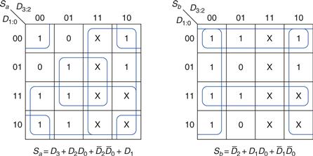
Figure 2.53 K-map solution with don’t cares
2.7.4 The Big Picture
Boolean algebra and Karnaugh maps are two methods of logic simplification. Ultimately, the goal is to find a low-cost method of implementing a particular logic function.
In modern engineering practice, computer programs called logic synthesizers produce simplified circuits from a description of the logic function, as we will see in Chapter 4. For large problems, logic synthesizers are much more efficient than humans. For small problems, a human with a bit of experience can find a good solution by inspection. Neither of the authors has ever used a Karnaugh map in real life to solve a practical problem. But the insight gained from the principles underlying Karnaugh maps is valuable. And Karnaugh maps often appear at job interviews!
2.8 Combinational Building Blocks
Combinational logic is often grouped into larger building blocks to build more complex systems. This is an application of the principle of abstraction, hiding the unnecessary gate-level details to emphasize the function of the building block. We have already studied three such building blocks: full adders (from Section 2.1), priority circuits (from Section 2.4), and seven-segment display decoders (from Section 2.7). This section introduces two more commonly used building blocks: multiplexers and decoders. Chapter 5 covers other combinational building blocks.
2.8.1 Multiplexers
Multiplexers are among the most commonly used combinational circuits. They choose an output from among several possible inputs based on the value of a select signal. A multiplexer is sometimes affectionately called a mux.
2:1 Multiplexer
Figure 2.54 shows the schematic and truth table for a 2:1 multiplexer with two data inputs D0 and D1, a select input S, and one output Y. The multiplexer chooses between the two data inputs based on the select: if S = 0, Y = D0, and if S = 1, Y = D1. S is also called a control signal because it controls what the multiplexer does.
Shorting together the outputs of multiple gates technically violates the rules for combinational circuits given in Section 2.1. But because exactly one of the outputs is driven at any time, this exception is allowed.
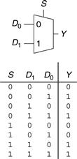
Figure 2.54 2:1 multiplexer symbol and truth table
A 2:1 multiplexer can be built from sum-of-products logic as shown in Figure 2.55. The Boolean equation for the multiplexer may be derived with a Karnaugh map or read off by inspection (Y is 1 if S = 0 AND D0 is 1 OR if S = 1 AND D1 is 1).
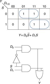
Figure 2.55 2:1 multiplexer implementation using two-level logic
Alternatively, multiplexers can be built from tristate buffers as shown in Figure 2.56. The tristate enables are arranged such that, at all times, exactly one tristate buffer is active. When S = 0, tristate T0 is enabled, allowing D0 to flow to Y. When S = 1, tristate T1 is enabled, allowing D1 to flow to Y.
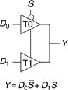
Figure 2.56 Multiplexer using tristate buffers
Wider Multiplexers
A 4:1 multiplexer has four data inputs and one output, as shown in Figure 2.57. Two select signals are needed to choose among the four data inputs. The 4:1 multiplexer can be built using sum-of-products logic, tristates, or multiple 2:1 multiplexers, as shown in Figure 2.58.

Figure 2.57 4:1 multiplexer
The product terms enabling the tristates can be formed using AND gates and inverters. They can also be formed using a decoder, which we will introduce in Section 2.8.2.
Wider multiplexers, such as 8:1 and 16:1 multiplexers, can be built by expanding the methods shown in Figure 2.58. In general, an N:1 multiplexer needs log2N select lines. Again, the best implementation choice depends on the target technology.

Figure 2.58 4:1 multiplexer implementations: (a) two-level logic, (b) tristates, (c) hierarchical
Multiplexer Logic
Multiplexers can be used as lookup tables to perform logic functions. Figure 2.59 shows a 4:1 multiplexer used to implement a two-input AND gate. The inputs, A and B, serve as select lines. The multiplexer data inputs are connected to 0 or 1 according to the corresponding row of the truth table. In general, a 2N-input multiplexer can be programmed to perform any N-input logic function by applying 0’s and 1’s to the appropriate data inputs. Indeed, by changing the data inputs, the multiplexer can be reprogrammed to perform a different function.

Figure 2.59 4:1 multiplexer implementation of two-input AND function
With a little cleverness, we can cut the multiplexer size in half, using only a 2N–1-input multiplexer to perform any N-input logic function. The strategy is to provide one of the literals, as well as 0’s and 1’s, to the multiplexer data inputs.
To illustrate this principle, Figure 2.60 shows two-input AND and XOR functions implemented with 2:1 multiplexers. We start with an ordinary truth table, and then combine pairs of rows to eliminate the rightmost input variable by expressing the output in terms of this variable. For example, in the case of AND, when A = 0, Y = 0, regardless of B. When A = 1, Y = 0 if B = 0 and Y = 1 if B = 1, so Y = B. We then use the multiplexer as a lookup table according to the new, smaller truth table.
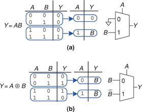
Figure 2.60 Multiplexer logic using variable inputs
Example 2.12 Logic with Multiplexers
Alyssa P. Hacker needs to implement the function ![]() to finish her senior project, but when she looks in her lab kit, the only part she has left is an 8:1 multiplexer. How does she implement the function?
to finish her senior project, but when she looks in her lab kit, the only part she has left is an 8:1 multiplexer. How does she implement the function?
Solution
Figure 2.61 shows Alyssa’s implementation using a single 8:1 multiplexer. The multiplexer acts as a lookup table where each row in the truth table corresponds to a multiplexer input.
Figure 2.61 Alyssa’s circuit: (a) truth table, (b) 8:1 multiplexer implementation
Example 2.13 Logic with Multiplexers, Reprised
Alyssa turns on her circuit one more time before the final presentation and blows up the 8:1 multiplexer. (She accidently powered it with 20 V instead of 5 V after not sleeping all night.) She begs her friends for spare parts and they give her a 4:1 multiplexer and an inverter. Can she build her circuit with only these parts?
Solution
Alyssa reduces her truth table to four rows by letting the output depend on C. (She could also have chosen to rearrange the columns of the truth table to let the output depend on A or B.) Figure 2.62 shows the new design.
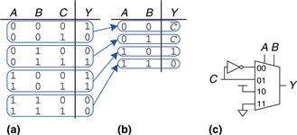
Figure 2.62 Alyssa’s new circuit
2.8.2 Decoders
A decoder has N inputs and 2N outputs. It asserts exactly one of its outputs depending on the input combination. Figure 2.63 shows a 2:4 decoder. When A1:0 = 00, Y0 is 1. When A1:0 = 01, Y1 is 1. And so forth. The outputs are called one-hot, because exactly one is “hot” (HIGH) at a given time.

Figure 2.63 2:4 decoder
Example 2.14 Decoder Implementation
Implement a 2:4 decoder with AND, OR, and NOT gates.
Solution
Figure 2.64 shows an implementation for the 2:4 decoder using four AND gates. Each gate depends on either the true or the complementary form of each input. In general, an N:2N decoder can be constructed from 2N N-input AND gates that accept the various combinations of true or complementary inputs. Each output in a decoder represents a single minterm. For example, Y0 represents the minterm ![]() This fact will be handy when using decoders with other digital building blocks.
This fact will be handy when using decoders with other digital building blocks.
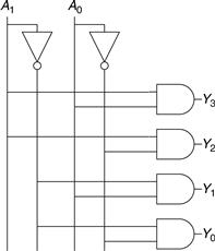
Figure 2.64 2:4 decoder implementation
Decoder Logic
Decoders can be combined with OR gates to build logic functions. Figure 2.65 shows the two-input XNOR function using a 2:4 decoder and a single OR gate. Because each output of a decoder represents a single minterm, the function is built as the OR of all the minterms in the function. In Figure 2.65, ![]()
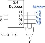
Figure 2.65 Logic function using decoder
When using decoders to build logic, it is easiest to express functions as a truth table or in canonical sum-of-products form. An N-input function with M 1’s in the truth table can be built with an N:2N decoder and an M-input OR gate attached to all of the minterms containing 1’s in the truth table. This concept will be applied to the building of Read Only Memories (ROMs) in Section 5.5.6.
2.9 Timing
In previous sections, we have been concerned primarily with whether the circuit works—ideally, using the fewest gates. However, as any seasoned circuit designer will attest, one of the most challenging issues in circuit design is timing: making a circuit run fast.
An output takes time to change in response to an input change. Figure 2.66 shows the delay between an input change and the subsequent output change for a buffer. The figure is called a timing diagram; it portrays the transient response of the buffer circuit when an input changes. The transition from LOW to HIGH is called the rising edge. Similarly, the transition from HIGH to LOW (not shown in the figure) is called the falling edge. The blue arrow indicates that the rising edge of Y is caused by the rising edge of A. We measure delay from the 50% point of the input signal, A, to the 50% point of the output signal, Y. The 50% point is the point at which the signal is half-way (50%) between its LOW and HIGH values as it transitions.
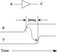
Figure 2.66 Circuit delay
2.9.1 Propagation and Contamination Delay
Combinational logic is characterized by its propagation delay and contamination delay. The propagation delay tpd is the maximum time from when an input changes until the output or outputs reach their final value. The contamination delay tcd is the minimum time from when an input changes until any output starts to change its value.
When designers speak of calculating the delay of a circuit, they generally are referring to the worst-case value (the propagation delay), unless it is clear otherwise from the context.
Figure 2.67 illustrates a buffer’s propagation delay and contamination delay in blue and gray, respectively. The figure shows that A is initially either HIGH or LOW and changes to the other state at a particular time; we are interested only in the fact that it changes, not what value it has. In response, Y changes some time later. The arcs indicate that Y may start to change tcd after A transitions and that Y definitely settles to its new value within tpd.
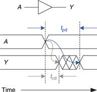
Figure 2.67 Propagation and contamination delay
The underlying causes of delay in circuits include the time required to charge the capacitance in a circuit and the speed of light. tpd and tcd may be different for many reasons, including
![]() different rising and falling delays
different rising and falling delays
![]() multiple inputs and outputs, some of which are faster than others
multiple inputs and outputs, some of which are faster than others
Calculating tpd and tcd requires delving into the lower levels of abstraction beyond the scope of this book. However, manufacturers normally supply data sheets specifying these delays for each gate.
Circuit delays are ordinarily on the order of picoseconds (1 ps = 10−12 seconds) to nanoseconds (1 ns = 10−9 seconds). Trillions of picoseconds have elapsed in the time you spent reading this sidebar.
Along with the factors already listed, propagation and contamination delays are also determined by the path a signal takes from input to output. Figure 2.68 shows a four-input logic circuit. The critical path, shown in blue, is the path from input A or B to output Y. It is the longest, and therefore the slowest, path, because the input travels through three gates to the output. This path is critical because it limits the speed at which the circuit operates. The short path through the circuit, shown in gray, is from input D to output Y. This is the shortest, and therefore the fastest, path through the circuit, because the input travels through only a single gate to the output.
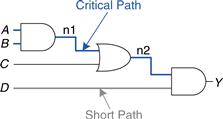
Figure 2.68 Short path and critical path
The propagation delay of a combinational circuit is the sum of the propagation delays through each element on the critical path. The contamination delay is the sum of the contamination delays through each element on the short path. These delays are illustrated in Figure 2.69 and are described by the following equations:
Although we are ignoring wire delay in this analysis, digital circuits are now so fast that the delay of long wires can be as important as the delay of the gates. The speed of light delay in wires is covered in Appendix A.
![]() (2.8)
(2.8)
![]() (2.9)
(2.9)
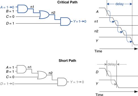
Figure 2.69 Critical and short path waveforms
Example 2.15 Finding Delays
Ben Bitdiddle needs to find the propagation delay and contamination delay of the circuit shown in Figure 2.70. According to his data book, each gate has a propagation delay of 100 picoseconds (ps) and a contamination delay of 60 ps.

Figure 2.70 Ben’s circuit
Solution
Ben begins by finding the critical path and the shortest path through the circuit. The critical path, highlighted in blue in Figure 2.71, is from input A or B through three gates to the output Y. Hence, tpd is three times the propagation delay of a single gate, or 300 ps.

Figure 2.71 Ben’s critical path
The shortest path, shown in gray in Figure 2.72, is from input C, D, or E through two gates to the output Y. There are only two gates in the shortest path, so tcd is 120 ps.

Figure 2.72 Ben’s shortest path
Example 2.16 Multiplexer Timing
Control-Critical vs. Data-Critical
Compare the worst-case timing of the three four-input multiplexer designs shown in Figure 2.58 in Section 2.8.1. Table 2.7 lists the propagation delays for the components. What is the critical path for each design? Given your timing analysis, why might you choose one design over the other?
Table 2.7 Timing specifications for multiplexer circuit elements
| Gate | tpd (ps) |
| NOT | 30 |
| 2-input AND | 60 |
| 3-input AND | 80 |
| 4-input OR | 90 |
| tristate (A to Y) | 50 |
| tristate (enable to Y) | 35 |
Solution
One of the critical paths for each of the three design options is highlighted in blue in Figures 2.73 and 2.74. tpd_sy indicates the propagation delay from input S to output Y; tpd_dy indicates the propagation delay from input D to output Y; tpd is the worst of the two: max(tpd_sy, tpd_dy).

Figure 2.73 4:1 multiplexer propagation delays: (a) two-level logic, (b) tristate
For both the two-level logic and tristate implementations in Figure 2.73, the critical path is from one of the control signals S to the output Y: tpd = tpd_sy. These circuits are control critical, because the critical path is from the control signals to the output. Any additional delay in the control signals will add directly to the worst-case delay. The delay from D to Y in Figure 2.73(b) is only 50 ps, compared with the delay from S to Y of 125 ps.
Figure 2.74 shows the hierarchical implementation of the 4:1 multiplexer using two stages of 2:1 multiplexers. The critical path is from any of the D inputs to the output. This circuit is data critical, because the critical path is from the data input to the output: tpd = tpd_dy.
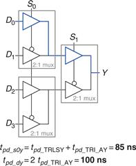
Figure 2.74 4:1 multiplexer propagation delays: hierarchical using 2:1 multiplexers
If data inputs arrive well before the control inputs, we would prefer the design with the shortest control-to-output delay (the hierarchical design in Figure 2.74). Similarly, if the control inputs arrive well before the data inputs, we would prefer the design with the shortest data-to-output delay (the tristate design in Figure 2.73(b)).
The best choice depends not only on the critical path through the circuit and the input arrival times, but also on the power, cost, and availability of parts.
2.9.2 Glitches
So far we have discussed the case where a single input transition causes a single output transition. However, it is possible that a single input transition can cause multiple output transitions. These are called glitches or hazards. Although glitches usually don’t cause problems, it is important to realize that they exist and recognize them when looking at timing diagrams. Figure 2.75 shows a circuit with a glitch and the Karnaugh map of the circuit.

Figure 2.75 Circuit with a glitch
The Boolean equation is correctly minimized, but let’s look at what happens when A = 0, C = 1, and B transitions from 1 to 0. Figure 2.76 (see page 94) illustrates this scenario. The short path (shown in gray) goes through two gates, the AND and OR gates. The critical path (shown in blue) goes through an inverter and two gates, the AND and OR gates.
Hazards have another meaning related to microarchitecture in Chapter 7, so we will stick with the term glitches for multiple output transitions to avoid confusion.
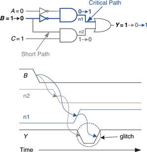
Figure 2.76 Timing of a glitch
As B transitions from 1 to 0, n2 (on the short path) falls before n1 (on the critical path) can rise. Until n1 rises, the two inputs to the OR gate are 0, and the output Y drops to 0. When n1 eventually rises, Y returns to 1. As shown in the timing diagram of Figure 2.76, Y starts at 1 and ends at 1 but momentarily glitches to 0.
As long as we wait for the propagation delay to elapse before we depend on the output, glitches are not a problem, because the output eventually settles to the right answer.
If we choose to, we can avoid this glitch by adding another gate to the implementation. This is easiest to understand in terms of the K-map. Figure 2.77 shows how an input transition on B from ABC = 001 to ABC = 011 moves from one prime implicant circle to another. The transition across the boundary of two prime implicants in the K-map indicates a possible glitch.
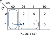
Figure 2.77 Input change crosses implicant boundary
As we saw from the timing diagram in Figure 2.76, if the circuitry implementing one of the prime implicants turns off before the circuitry of the other prime implicant can turn on, there is a glitch. To fix this, we add another circle that covers that prime implicant boundary, as shown in Figure 2.78. You might recognize this as the consensus theorem, where the added term, ![]() , is the consensus or redundant term.
, is the consensus or redundant term.
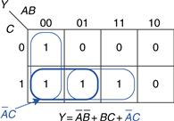
Figure 2.78 K-map without glitch
Figure 2.79 shows the glitch-proof circuit. The added AND gate is highlighted in blue. Now a transition on B when A = 0 and C = 1 does not cause a glitch on the output, because the blue AND gate outputs 1 throughout the transition.
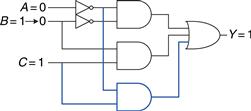
Figure 2.79 Circuit without glitch
In general, a glitch can occur when a change in a single variable crosses the boundary between two prime implicants in a K-map. We can eliminate the glitch by adding redundant implicants to the K-map to cover these boundaries. This of course comes at the cost of extra hardware.
However, simultaneous transitions on multiple inputs can also cause glitches. These glitches cannot be fixed by adding hardware. Because the vast majority of interesting systems have simultaneous (or near-simultaneous) transitions on multiple inputs, glitches are a fact of life in most circuits. Although we have shown how to eliminate one kind of glitch, the point of discussing glitches is not to eliminate them but to be aware that they exist. This is especially important when looking at timing diagrams on a simulator or oscilloscope.
2.10 Summary
A digital circuit is a module with discrete-valued inputs and outputs and a specification describing the function and timing of the module. This chapter has focused on combinational circuits, circuits whose outputs depend only on the current values of the inputs.
The function of a combinational circuit can be given by a truth table or a Boolean equation. The Boolean equation for any truth table can be obtained systematically using sum-of-products or product-of-sums form. In sum-of-products form, the function is written as the sum (OR) of one or more implicants. Implicants are the product (AND) of literals. Literals are the true or complementary forms of the input variables.
Boolean equations can be simplified using the rules of Boolean algebra. In particular, they can be simplified into minimal sum-of-products form by combining implicants that differ only in the true and complementary forms of one of the literals: ![]() Karnaugh maps are a visual tool for minimizing functions of up to four variables. With practice, designers can usually simplify functions of a few variables by inspection. Computer-aided design tools are used for more complicated functions; such methods and tools are discussed in Chapter 4.
Karnaugh maps are a visual tool for minimizing functions of up to four variables. With practice, designers can usually simplify functions of a few variables by inspection. Computer-aided design tools are used for more complicated functions; such methods and tools are discussed in Chapter 4.
Logic gates are connected to create combinational circuits that perform the desired function. Any function in sum-of-products form can be built using two-level logic: NOT gates form the complements of the inputs, AND gates form the products, and OR gates form the sum. Depending on the function and the building blocks available, multilevel logic implementations with various types of gates may be more efficient. For example, CMOS circuits favor NAND and NOR gates because these gates can be built directly from CMOS transistors without requiring extra NOT gates. When using NAND and NOR gates, bubble pushing is helpful to keep track of the inversions.
Logic gates are combined to produce larger circuits such as multiplexers, decoders, and priority circuits. A multiplexer chooses one of the data inputs based on the select input. A decoder sets one of the outputs HIGH according to the inputs. A priority circuit produces an output indicating the highest priority input. These circuits are all examples of combinational building blocks. Chapter 5 will introduce more building blocks, including other arithmetic circuits. These building blocks will be used extensively to build a microprocessor in Chapter 7.
The timing specification of a combinational circuit consists of the propagation and contamination delays through the circuit. These indicate the longest and shortest times between an input change and the consequent output change. Calculating the propagation delay of a circuit involves identifying the critical path through the circuit, then adding up the propagation delays of each element along that path. There are many different ways to implement complicated combinational circuits; these ways offer trade-offs between speed and cost.
The next chapter will move to sequential circuits, whose outputs depend on current as well as previous values of the inputs. In other words, sequential circuits have memory of the past.
Exercises
Exercise 2.1 Write a Boolean equation in sum-of-products canonical form for each of the truth tables in Figure 2.80.
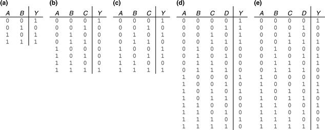
Figure 2.80 Truth tables for Exercises 2.1 and 2.3
Exercise 2.2 Write a Boolean equation in sum-of-products canonical form for each of the truth tables in Figure 2.81.

Figure 2.81 Truth tables for Exercises 2.2 and 2.4
Exercise 2.3 Write a Boolean equation in product-of-sums canonical form for the truth tables in Figure 2.80.
Exercise 2.4 Write a Boolean equation in product-of-sums canonical form for the truth tables in Figure 2.81.
Exercise 2.5 Minimize each of the Boolean equations from Exercise 2.1.
Exercise 2.6 Minimize each of the Boolean equations from Exercise 2.2.
Exercise 2.7 Sketch a reasonably simple combinational circuit implementing each of the functions from Exercise 2.5. Reasonably simple means that you are not wasteful of gates, but you don’t waste vast amounts of time checking every possible implementation of the circuit either.
Exercise 2.8 Sketch a reasonably simple combinational circuit implementing each of the functions from Exercise 2.6.
Exercise 2.9 Repeat Exercise 2.7 using only NOT gates and AND and OR gates.
Exercise 2.10 Repeat Exercise 2.8 using only NOT gates and AND and OR gates.
Exercise 2.11 Repeat Exercise 2.7 using only NOT gates and NAND and NOR gates.
Exercise 2.12 Repeat Exercise 2.8 using only NOT gates and NAND and NOR gates.
Exercise 2.13 Simplify the following Boolean equations using Boolean theorems. Check for correctness using a truth table or K-map.
Exercise 2.14 Simplify the following Boolean equations using Boolean theorems. Check for correctness using a truth table or K-map.
Exercise 2.15 Sketch a reasonably simple combinational circuit implementing each of the functions from Exercise 2.13.
Exercise 2.16 Sketch a reasonably simple combinational circuit implementing each of the functions from Exercise 2.14.
Exercise 2.17 Simplify each of the following Boolean equations. Sketch a reasonably simple combinational circuit implementing the simplified equation.
Exercise 2.18 Simplify each of the following Boolean equations. Sketch a reasonably simple combinational circuit implementing the simplified equation.
Exercise 2.19 Give an example of a truth table requiring between 3 billion and 5 billion rows that can be constructed using fewer than 40 (but at least 1) two-input gates.
Exercise 2.20 Give an example of a circuit with a cyclic path that is nevertheless combinational.
Exercise 2.21 Alyssa P. Hacker says that any Boolean function can be written in minimal sum-of-products form as the sum of all of the prime implicants of the function. Ben Bitdiddle says that there are some functions whose minimal equation does not involve all of the prime implicants. Explain why Alyssa is right or provide a counterexample demonstrating Ben’s point.
Exercise 2.22 Prove that the following theorems are true using perfect induction. You need not prove their duals.
Exercise 2.23 Prove De Morgan’s Theorem (T12) for three variables, B2, B1, B0, using perfect induction.
Exercise 2.24 Write Boolean equations for the circuit in Figure 2.82. You need not minimize the equations.
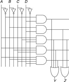
Figure 2.82 Circuit schematic
Exercise 2.25 Minimize the Boolean equations from Exercise 2.24 and sketch an improved circuit with the same function.
Exercise 2.26 Using De Morgan equivalent gates and bubble pushing methods, redraw the circuit in Figure 2.83 so that you can find the Boolean equation by inspection. Write the Boolean equation.
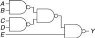
Figure 2.83 Circuit schematic
Exercise 2.27 Repeat Exercise 2.26 for the circuit in Figure 2.84.
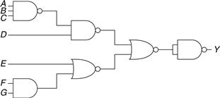
Figure 2.84 Circuit schematic
Exercise 2.28 Find a minimal Boolean equation for the function in Figure 2.85. Remember to take advantage of the don’t care entries.

Figure 2.85 Truth table for Exercise 2.28
Exercise 2.29 Sketch a circuit for the function from Exercise 2.28.
Exercise 2.30 Does your circuit from Exercise 2.29 have any potential glitches when one of the inputs changes? If not, explain why not. If so, show how to modify the circuit to eliminate the glitches.
Exercise 2.31 Find a minimal Boolean equation for the function in Figure 2.86. Remember to take advantage of the don’t care entries.
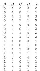
Figure 2.86 Truth table for Exercise 2.31
Exercise 2.32 Sketch a circuit for the function from Exercise 2.31.
Exercise 2.33 Ben Bitdiddle will enjoy his picnic on sunny days that have no ants. He will also enjoy his picnic any day he sees a hummingbird, as well as on days where there are ants and ladybugs. Write a Boolean equation for his enjoyment (E) in terms of sun (S), ants (A), hummingbirds (H), and ladybugs (L).
Exercise 2.34 Complete the design of the seven-segment decoder segments Sc through Sg (see Example 2.10):
(a) Derive Boolean equations for the outputs Sc through Sg assuming that inputs greater than 9 must produce blank (0) outputs.
(b) Derive Boolean equations for the outputs Sc through Sg assuming that inputs greater than 9 are don’t cares.
(c) Sketch a reasonably simple gate-level implementation of part (b). Multiple outputs can share gates where appropriate.
Exercise 2.35 A circuit has four inputs and two outputs. The inputs Α3:0 represent a number from 0 to 15. Output P should be TRUE if the number is prime (0 and 1 are not prime, but 2, 3, 5, and so on, are prime). Output D should be TRUE if the number is divisible by 3. Give simplified Boolean equations for each output and sketch a circuit.
Exercise 2.36 A priority encoder has 2N inputs. It produces an N-bit binary output indicating the most significant bit of the input that is TRUE, or 0 if none of the inputs are TRUE. It also produces an output NONE that is TRUE if none of the inputs are TRUE. Design an eight-input priority encoder with inputs A7:0 and outputs Y2.0 and NONE. For example, if the input is 00100000, the output Y should be 101 and NONE should be 0. Give a simplified Boolean equation for each output, and sketch a schematic.
Exercise 2.37 Design a modified priority encoder (see Exercise 2.36) that receives an 8-bit input, A7:0, and produces two 3-bit outputs, Y2:0 and Z2:0 Y indicates the most significant bit of the input that is TRUE. Z indicates the second most significant bit of the input that is TRUE. Y should be 0 if none of the inputs are TRUE. Z should be 0 if no more than one of the inputs is TRUE. Give a simplified Boolean equation for each output, and sketch a schematic.
Exercise 2.38 An M-bit thermometer code for the number k consists of k 1’s in the least significant bit positions and M – k 0’s in all the more significant bit positions. A binary-to-thermometer code converter has N inputs and 2N–1 outputs. It produces a 2N–1 bit thermometer code for the number specified by the input. For example, if the input is 110, the output should be 0111111. Design a 3:7 binary-to-thermometer code converter. Give a simplified Boolean equation for each output, and sketch a schematic.
Exercise 2.39 Write a minimized Boolean equation for the function performed by the circuit in Figure 2.87.
Figure 2.87 Multiplexer circuit
Exercise 2.40 Write a minimized Boolean equation for the function performed by the circuit in Figure 2.88.
Figure 2.88 Multiplexer circuit
Exercise 2.41 Implement the function from Figure 2.80(b) using
Exercise 2.42 Implement the function from Exercise 2.17(a) using
Exercise 2.43 Determine the propagation delay and contamination delay of the circuit in Figure 2.83. Use the gate delays given in Table 2.8.
Exercise 2.44 Determine the propagation delay and contamination delay of the circuit in Figure 2.84. Use the gate delays given in Table 2.8.
Table 2.8 Gate delays for Exercises 2.43–2.47
| Gate | tpd (ps) | tcd (ps) |
| NOT | 15 | 10 |
| 2-input NAND | 20 | 15 |
| 3-input NAND | 30 | 25 |
| 2-input NOR | 30 | 25 |
| 3-input NOR | 45 | 35 |
| 2-input AND | 30 | 25 |
| 3-input AND | 40 | 30 |
| 2-input OR | 40 | 30 |
| 3-input OR | 55 | 45 |
| 2-input XOR | 60 | 40 |
Exercise 2.45 Sketch a schematic for a fast 3:8 decoder. Suppose gate delays are given in Table 2.8 (and only the gates in that table are available). Design your decoder to have the shortest possible critical path, and indicate what that path is. What are its propagation delay and contamination delay?
Exercise 2.46 Redesign the circuit from Exercise 2.35 to be as fast as possible. Use only the gates from Table 2.8. Sketch the new circuit and indicate the critical path. What are its propagation delay and contamination delay?
Exercise 2.47 Redesign the priority encoder from Exercise 2.36 to be as fast as possible. You may use any of the gates from Table 2.8. Sketch the new circuit and indicate the critical path. What are its propagation delay and contamination delay?
Exercise 2.48 Design an 8:1 multiplexer with the shortest possible delay from the data inputs to the output. You may use any of the gates from Table 2.7 on page 92. Sketch a schematic. Using the gate delays from the table, determine this delay.
Interview Questions
The following exercises present questions that have been asked at interviews for digital design jobs.
Question 2.1 Sketch a schematic for the two-input XOR function using only NAND gates. How few can you use?
Question 2.2 Design a circuit that will tell whether a given month has 31 days in it. The month is specified by a 4-bit input Α3:0. For example, if the inputs are 0001, the month is January, and if the inputs are 1100, the month is December. The circuit output Y should be HIGH only when the month specified by the inputs has 31 days in it. Write the simplified equation, and draw the circuit diagram using a minimum number of gates. (Hint: Remember to take advantage of don’t cares.)
Question 2.3 What is a tristate buffer? How and why is it used?
Question 2.4 A gate or set of gates is universal if it can be used to construct any Boolean function. For example, the set {AND, OR, NOT} is universal.
(a) Is an AND gate by itself universal? Why or why not?
Question 2.5 Explain why a circuit’s contamination delay might be less than (instead of equal to) its propagation delay.
1 Black light, twinkies, and beer.