
SystemVerilog
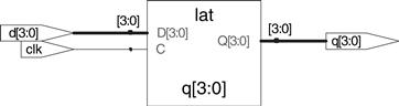
module latch(input logic clk,
input logic [3:0] d,
output logic [3:0] q);
always_latch
if (clk) q <= d;
endmodule
always_latch is equivalent to always @(clk, d) and is the preferred idiom for describing a latch in SystemVerilog. It evaluates any time clk or d changes. If clk is HIGH, d flows through to q, so this code describes a positive level sensitive latch. Otherwise, q keeps its old value. SystemVerilog can generate a warning if the always_latch block doesn’t imply a latch.
VHDL
library IEEE; use IEEE.STD_LOGIC_1164.all;
entity latch is
port(clk: in STD_LOGIC;
d: in STD_LOGIC_VECTOR(3 downto 0);
q: out STD_LOGIC_VECTOR(3 downto 0));
end;
architecture synth of latch is
begin
process(clk, d) begin
if clk = ‘1’ then
q <= d;
end if;
end process;
end;
The sensitivity list contains both clk and d, so the process evaluates anytime clk or d changes. If clk is HIGH, d flows through to q.
HDL Example 4.22 Inverter Using always/process
SystemVerilog
module inv(input logic [3:0] a,
output logic [3:0] y);
always_comb
y = ~a;
endmodule
always_comb reevaluates the statements inside the always statement any time any of the signals on the right hand side of <= or = in the always statement change. In this case, it is equivalent to always @(a), but is better because it avoids mistakes if signals in the always statement are renamed or added. If the code inside the always block is not combinational logic, SystemVerilog will report a warning. always_comb is equivalent to always @(*), but is preferred in SystemVerilog.
The = in the always statement is called a blocking assignment, in contrast to the <= nonblocking assignment. In SystemVerilog, it is good practice to use blocking assignments for combinational logic and nonblocking assignments for sequential logic. This will be discussed further in Section 4.5.4.
VHDL
library IEEE; use IEEE.STD_LOGIC_1164.all;
entity inv is
port(a: in STD_LOGIC_VECTOR(3 downto 0);
y: out STD_LOGIC_VECTOR(3 downto 0));
end;
architecture proc of inv is
begin
process(all) begin
y <= not a;
end process;
end;
process(all) reevaluates the statements inside the process any time any of the signals in the process change. It is equivalent to process(a) but is better because it avoids mistakes if signals in the process are renamed or added.
The begin and end process statements are required in VHDL even though the process contains only one assignment.
HDLs support blocking and nonblocking assignments in an always/process statement. A group of blocking assignments are evaluated in the order in which they appear in the code, just as one would expect in a standard programming language. A group of nonblocking assignments are evaluated concurrently; all of the statements are evaluated before any of the signals on the left hand sides are updated.
HDL Example 4.23 defines a full adder using intermediate signals p and g to compute s and cout. It produces the same circuit from Figure 4.8, but uses always/process statements in place of assignment statements.
These two examples are poor applications of always/process statements for modeling combinational logic because they require more lines than the equivalent approach with assignment statements from HDL Examples 4.2 and 4.7. However, case and if statements are convenient for modeling more complicated combinational logic. case and if statements must appear within always/process statements and are examined in the next sections.
SystemVerilog
In a SystemVerilog always statement, = indicates a blocking assignment and <= indicates a nonblocking assignment (also called a concurrent assignment).
Do not confuse either type with continuous assignment using the assign statement. assign statements must be used outside always statements and are also evaluated concurrently.
VHDL
In a VHDL process statement, : = indicates a blocking assignment and <= indicates a nonblocking assignment (also called a concurrent assignment). This is the first section where : = is introduced.
Nonblocking assignments are made to outputs and to signals. Blocking assignments are made to variables, which are declared in process statements (see HDL Example 4.23). <= can also appear outside process statements, where it is also evaluated concurrently.
HDL Example 4.23 Full Adder Using always/process
SystemVerilog
module fulladder(input logic a, b, cin,
output logic s, cout);
logic p, g;
always_comb
begin
p = a ^ b; // blocking
g = a & b; // blocking
s = p ^ cin; // blocking
cout = g | (p & cin); // blocking
end
endmodule
In this case, always @(a, b, cin) would have been equivalent to always_comb. However, always_comb is better because it avoids common mistakes of missing signals in the sensitivity list.
For reasons that will be discussed in Section 4.5.4, it is best to use blocking assignments for combinational logic. This example uses blocking assignments, first computing p, then g, then s, and finally cout.
VHDL
library IEEE; use IEEE.STD_LOGIC_1164.all;
entity fulladder is
port(a, b, cin: in STD_LOGIC;
s, cout: out STD_LOGIC);
end;
architecture synth of fulladder is
begin
process(all)
variable p, g: STD_LOGIC;
begin
p := a xor b; –– blocking
g := a and b; –– blocking
s <= p xor cin;
cout <= g or (p and cin);
end process;
end;
In this case, process(a, b, cin) would have been equivalent to process(all). However, process(all) is better because it avoids common mistakes of missing signals in the sensitivity list.
For reasons that will be discussed in Section 4.5.4, it is best to use blocking assignments for intermediate variables in combinational logic. This example uses blocking assignments for p and g so that they get their new values before being used to compute s and cout that depend on them.
Because p and g appear on the left hand side of a blocking assignment (:=) in a process statement, they must be declared to be variable rather than signal. The variable declaration appears before the begin in the process where the variable is used.
4.5.1 Case Statements
A better application of using the always/process statement for combinational logic is a seven-segment display decoder that takes advantage of the case statement that must appear inside an always/process statement.
As you might have noticed in the seven-segment display decoder of Example 2.10, the design process for large blocks of combinational logic is tedious and prone to error. HDLs offer a great improvement, allowing you to specify the function at a higher level of abstraction, and then automatically synthesize the function into gates. HDL Example 4.24 uses case statements to describe a seven-segment display decoder based on its truth table. The case statement performs different actions depending on the value of its input. A case statement implies combinational logic if all possible input combinations are defined; otherwise it implies sequential logic, because the output will keep its old value in the undefined cases.
HDL Example 4.24 Seven-Segment Display Decoder
SystemVerilog
module sevenseg(input logic [3:0] data,
output logic [6:0] segments);
always_comb
case(data)
// abc_defg
0: segments = 7’b111_1110;
1: segments = 7’b011_0000;
2: segments = 7’b110_1101;
3: segments = 7’b111_1001;
4: segments = 7’b011_0011;
5: segments = 7’b101_1011;
6: segments = 7’b101_1111;
7: segments = 7’b111_0000;
8: segments = 7’b111_1111;
9: segments = 7’b111_0011;
default: segments = 7’b000_0000;
endcase
endmodule
The case statement checks the value of data. When data is 0, the statement performs the action after the colon, setting segments to 1111110. The case statement similarly checks other data values up to 9 (note the use of the default base, base 10).
The default clause is a convenient way to define the output for all cases not explicitly listed, guaranteeing combinational logic.
In SystemVerilog, case statements must appear inside always statements.
VHDL
library IEEE; use IEEE.STD_LOGIC_1164.all;
entity seven_seg_decoder is
port(data: in STD_LOGIC_VECTOR(3 downto 0);
segments: out STD_LOGIC_VECTOR(6 downto 0));
end;
architecture synth of seven_seg_decoder is
begin
process(all) begin
case data is
–– abcdefg
when X"0" => segments <= "1111110";
when X"1" => segments <= "0110000";
when X"2" => segments <= "1101101";
when X"3" => segments <= "1111001";
when X"4" => segments <= "0110011";
when X"5" => segments <= "1011011";
when X"6" => segments <= "1011111";
when X"7" => segments <= "1110000";
when X"8" => segments <= "1111111";
when X"9" => segments <= "1110011";
when others => segments <= “0000000”;
end case;
end process;
end;
The case statement checks the value of data. When data is 0, the statement performs the action after the =>, setting segments to 1111110. The case statement similarly checks other data values up to 9 (note the use of X for hexadecimal numbers). The others clause is a convenient way to define the output for all cases not explicitly listed, guaranteeing combinational logic.
Unlike SystemVerilog, VHDL supports selected signal assignment statements (see HDL Example 4.6), which are much like case statements but can appear outside processes. Thus, there is less reason to use processes to describe combinational logic.

Synplify Premier synthesizes the seven-segment display decoder into a read-only memory (ROM) containing the 7 outputs for each of the 16 possible inputs. ROMs are discussed further in Section 5.5.6.
If the default or others clause were left out of the case statement, the decoder would have remembered its previous output anytime data were in the range of 10–15. This is strange behavior for hardware.
Ordinary decoders are also commonly written with case statements. HDL Example 4.25 describes a 3:8 decoder.
4.5.2 If Statements
always/process statements may also contain if statements. The if statement may be followed by an else statement. If all possible input combinations are handled, the statement implies combinational logic; otherwise, it produces sequential logic (like the latch in Section 4.4.5).
HDL Example 4.25 3:8 Decoder
SystemVerilog
module decoder3_8(input logic [2:0] a,
output logic [7:0] y);
always_comb
case(a)
3’b000: y = 8’b00000001;
3’b001: y = 8’b00000010;
3’b010: y = 8’b00000100;
3’b011: y = 8’b00001000;
3’b100: y = 8’b00010000;
3’b101: y = 8’b00100000;
3’b110: y = 8’b01000000;
3’b111: y = 8’b10000000;
default: y = 8’bxxxxxxxx;
endcase
endmodule
The default statement isn’t strictly necessary for logic synthesis in this case because all possible input combinations are defined, but it is prudent for simulation in case one of the inputs is an x or z.
VHDL
library IEEE; use IEEE.STD_LOGIC_1164.all;
entity decoder3_8 is
port(a: in STD_LOGIC_VECTOR(2 downto 0);
y: out STD_LOGIC_VECTOR(7 downto 0));
end;
architecture synth of decoder3_8 is
begin
process(all) begin
case a is
when "000" => y <= "00000001";
when "001" => y <= "00000010";
when "010" => y <= "00000100";
when "011" => y <= "00001000";
when "100" => y <= "00010000";
when "101" => y <= "00100000";
when "110" => y <= "01000000";
when "111" => y <= "10000000";
when others => y <= "XXXXXXXX";
end case;
end process;
end;
The others clause isn’t strictly necessary for logic synthesis in this case because all possible input combinations are defined, but it is prudent for simulation in case one of the inputs is an x, z, or u.
HDL Example 4.26 Priority Circuit
SystemVerilog
module priorityckt(input logic [3:0] a,
output logic [3:0] y);
always_comb
if (a[3]) y <= 4’b1000;
else if (a[2]) y <= 4’b0100;
else if (a[1]) y <= 4’b0010;
else if (a[0]) y <= 4’b0001;
else y <= 4’b0000;
endmodule
In SystemVerilog, if statements must appear inside of always statements.
VHDL
library IEEE; use IEEE.STD_LOGIC_1164.all;
entity priorityckt is
port(a: in STD_LOGIC_VECTOR(3 downto 0);
y: out STD_LOGIC_VECTOR(3 downto 0));
end;
architecture synth of priorityckt is
begin
process(all) begin
if a(3) then y <= "1000";
elsif a(2) then y <= "0100";
elsif a(1) then y <= "0010";
elsif a(0) then y <= "0001";
else y <= “0000”;
end if;
end process;
end;
Unlike SystemVerilog, VHDL supports conditional signal assignment statements (see HDL Example 4.6), which are much like if statements but can appear outside processes. Thus, there is less reason to use processes to describe combinational logic.
HDL Example 4.26 uses if statements to describe a priority circuit, defined in Section 2.4. Recall that an N-input priority circuit sets the output TRUE that corresponds to the most significant input that is TRUE.
4.5.3 Truth Tables with Don’t Cares
As examined in Section 2.7.3, truth tables may include don’t care’s to allow more logic simplification. HDL Example 4.27 shows how to describe a priority circuit with don’t cares.
Synplify Premier synthesizes a slightly different circuit for this module, shown in Figure 4.23, than it did for the priority circuit in Figure 4.22. However, the circuits are logically equivalent.
Figure 4.22 priorityckt synthesized circuit
Figure 4.23 priority_casez synthesized circuit
HDL Example 4.27 Priority Circuit Using don’t cares
SystemVerilog
module priority_casez(input logic [3:0] a,
output logic [3:0] y);
always_comb
casez(a)
4’b1???: y <= 4’b1000;
4’b01??: y <= 4’b0100;
4’b001?: y <= 4’b0010;
4’b0001: y <= 4’b0001;
default: y <= 4’b0000;
endcase
endmodule
The casez statement acts like a case statement except that it also recognizes ? as don’t care.
VHDL
library IEEE; use IEEE.STD_LOGIC_1164.all;
entity priority_casez is
port(a: in STD_LOGIC_VECTOR(3 downto 0);
y: out STD_LOGIC_VECTOR(3 downto 0));
end;
architecture dontcare of priority_casez is
begin
process(all) begin
case? a is
when "1---" => y <= "1000";
when "01--" => y <= "0100";
when "001-" => y <= "0010";
when "0001" => y <= "0001";
when others => y <= “0000”;
end case?;
end process;
end;
The case? statement acts like a case statement except that it also recognizes – as don’t care.
4.5.4 Blocking and Nonblocking Assignments
The guidelines on page 206 explain when and how to use each type of assignment. If these guidelines are not followed, it is possible to write code that appears to work in simulation but synthesizes to incorrect hardware. The optional remainder of this section explains the principles behind the guidelines.
Blocking and Nonblocking Assignment Guidelines
SystemVerilog
1. Use always_ff @(posedge clk) and nonblocking assignments to model synchronous sequential logic.
always_ff @(posedge clk)
begin
n1 <= d; // nonblocking
q <= n1; // nonblocking
end
2. Use continuous assignments to model simple combinational logic.
assign y = s ? d1 : d0;
3. Use always_comb and blocking assignments to model more complicated combinational logic where the always statement is helpful.
always_comb
begin
p = a ^ b; // blocking
g = a & b; // blocking
s = p ^ cin;
cout = g | (p & cin);
end
4. Do not make assignments to the same signal in more than one always statement or continuous assignment statement.
VHDL
1. Use process(clk) and nonblocking assignments to model synchronous sequential logic.
process(clk) begin
if rising_edge(clk) then
n1 <= d; –– nonblocking
q <= n1; –– nonblocking
end if;
end process;
2. Use concurrent assignments outside process statements to model simple combinational logic.
y <= d0 when s = ‘0’ else d1;
3. Use process(all) to model more complicated combinational logic where the process is helpful. Use blocking assignments for internal variables.
process(all)
variable p, g: STD_LOGIC;
begin
p := a xor b; –– blocking
g := a and b; –– blocking
s <= p xor cin;
cout <= g or (p and cin);
end process;
4. Do not make assignments to the same variable in more than one process or concurrent assignment statement.
Combinational Logic*
The full adder from HDL Example 4.23 is correctly modeled using blocking assignments. This section explores how it operates and how it would differ if nonblocking assignments had been used.
Imagine that a, b, and cin are all initially 0. p, g, s, and cout are thus 0 as well. At some time, a changes to 1, triggering the always/process statement. The four blocking assignments evaluate in the order shown here. (In the VHDL code, s and cout are assigned concurrently.) Note that p and g get their new values before s and cout are computed because of the blocking assignments. This is important because we want to compute s and cout using the new values of p and g.
In contrast, HDL Example 4.28 illustrates the use of nonblocking assignments.
Now consider the same case of a rising from 0 to 1 while b and cin are 0. The four nonblocking assignments evaluate concurrently:
HDL Example 4.28 Full Adder Using Nonblocking Assignments
SystemVerilog
// nonblocking assignments (not recommended)
module fulladder(input logic a, b, cin,
output logic s, cout);
logic p, g;
always_comb
begin
p <= a ^ b; // nonblocking
g <= a & b; // nonblocking
s <= p ^ cin;
cout <= g | (p & cin);
end
endmodule
VHDL
–– nonblocking assignments (not recommended)
library IEEE; use IEEE.STD_LOGIC_1164.all;
entity fulladder is
port(a, b, cin: in STD_LOGIC;
s, cout: out STD_LOGIC);
end;
architecture nonblocking of fulladder is
signal p, g: STD_LOGIC;
begin
process(all) begin
p <= a xor b; –– nonblocking
g <= a and b; –– nonblocking
s <= p xor cin;
cout <= g or (p and cin);
end process;
end;
Because p and g appear on the left hand side of a nonblocking assignment in a process statement, they must be declared to be signal rather than variable. The signal declaration appears before the begin in the architecture, not the process.
Observe that s is computed concurrently with p and hence uses the old value of p, not the new value. Therefore, s remains 0 rather than becoming 1. However, p does change from 0 to 1. This change triggers the always/process statement to evaluate a second time, as follows:
This time, p is already 1, so s correctly changes to 1. The nonblocking assignments eventually reach the right answer, but the always/process statement had to evaluate twice. This makes simulation slower, though it synthesizes to the same hardware.
Another drawback of nonblocking assignments in modeling combinational logic is that the HDL will produce the wrong result if you forget to include the intermediate variables in the sensitivity list.
Worse yet, some synthesis tools will synthesize the correct hardware even when a faulty sensitivity list causes incorrect simulation. This leads to a mismatch between the simulation results and what the hardware actually does.
SystemVerilog
If the sensitivity list of the always statement in HDL Example 4.28 were written as always @(a, b, cin) rather than always_ comb, then the statement would not reevaluate when p or g changes. In that case, s would be incorrectly left at 0, not 1.
VHDL
If the sensitivity list of the process statement in HDL Example 4.28 were written as process(a, b, cin) rather than process(all), then the statement would not reevaluate when p or g changes. In that case, s would be incorrectly left at 0, not 1.
Sequential Logic*
The synchronizer from HDL Example 4.20 is correctly modeled using nonblocking assignments. On the rising edge of the clock, d is copied to n1 at the same time that n1 is copied to q, so the code properly describes two registers. For example, suppose initially that d = 0, n1 = 1, and q = 0. On the rising edge of the clock, the following two assignments occur concurrently, so that after the clock edge, n1 = 0 and q = 1.
HDL Example 4.29 tries to describe the same module using blocking assignments. On the rising edge of clk, d is copied to n1. Then this new value of n1 is copied to q, resulting in d improperly appearing at both n1 and q. The assignments occur one after the other so that after the clock edge, q = n1 = 0.
HDL Example 4.29 Bad Synchronizer with Blocking Assignments
SystemVerilog
// Bad implementation of a synchronizer using blocking // assignments
module syncbad(input logic clk,
input logic d,
output logic q);
logic n1;
always_ff @(posedge clk)
begin
n1 = d; // blocking
q = n1; // blocking
end
endmodule
VHDL
–– Bad implementation of a synchronizer using blocking –– assignment
library IEEE; use IEEE.STD_LOGIC_1164.all;
entity syncbad is
port(clk: in STD_LOGIC;
d: in STD_LOGIC;
q: out STD_LOGIC);
end;
architecture bad of syncbad is
begin
process(clk)
variable n1: STD_LOGIC;
begin
if rising_edge(clk) then
n1 := d; - - blocking
q <= n1;
end if;
end process;
end;
Because n1 is invisible to the outside world and does not influence the behavior of q, the synthesizer optimizes it away entirely, as shown in Figure 4.24.
Figure 4.24 syncbad synthesized circuit
The moral of this illustration is to exclusively use nonblocking assignment in always/process statements when modeling sequential logic. With sufficient cleverness, such as reversing the orders of the assignments, you could make blocking assignments work correctly, but blocking assignments offer no advantages and only introduce the risk of unintended behavior. Certain sequential circuits will not work with blocking assignments no matter what the order.
4.6 Finite State Machines
Recall that a finite state machine (FSM) consists of a state register and two blocks of combinational logic to compute the next state and the output given the current state and the input, as was shown in Figure 3.22. HDL descriptions of state machines are correspondingly divided into three parts to model the state register, the next state logic, and the output logic.
HDL Example 4.30 Divide-By-3 Finite State Machine
SystemVerilog
module divideby3FSM(input logic clk,
input logic reset,
output logic y);
typedef enum logic [1:0] {S0, S1, S2} statetype;
statetype [1:0] state, nextstate;
// state register
always_ff @(posedge clk, posedge reset)
if (reset) state <= S0;
else state <= nextstate;
// next state logic
always_comb
case (state)
S0: nextstate <= S1;
S1: nextstate <= S2;
S2: nextstate <= S0;
default: nextstate <= S0;
endcase
// output logic
assign y = (state = = S0);
endmodule
The typedef statement defines statetype to be a two-bit logic value with three possibilities: S0, S1, or S2. state and nextstate are statetype signals.
The enumerated encodings default to numerical order: S0 = 00, S1 = 01, and S2 = 10. The encodings can be explicitly set by the user; however, the synthesis tool views them as suggestions, not requirements. For example, the following snippet encodes the states as 3-bit one-hot values:
typedef enum logic [2:0] {S0 = 3’b001, S1 = 3’b010, S2 = 3’b100} statetype;
Notice how a case statement is used to define the state transition table. Because the next state logic should be combinational, a default is necessary even though the state 2’b11 should never arise.
The output, y, is 1 when the state is S0. The equality comparison a == b evaluates to 1 if a equals b and 0 otherwise. The inequality comparison a != b does the inverse, evaluating to 1 if a does not equal b.
VHDL
library IEEE; use IEEE.STD_LOGIC_1164.all;
entity divideby3FSM is
port(clk, reset: in STD_LOGIC;
y: out STD_LOGIC);
end;
architecture synth of divideby3FSM is
type statetype is (S0, S1, S2);
signal state, nextstate: statetype;
begin
–– state register
process(clk, reset) begin
if reset then state <= S0;
elsif rising_edge(clk) then
state <= nextstate;
end if;
end process;
–– next state logic
nextstate <= S1 when state = S0 else
S2 when state = S1 else
S0;
–– output logic
y <= ‘1’ when state = S0 else ‘0’;
end;
This example defines a new enumeration data type, statetype, with three possibilities: S0, S1, and S2. state and nextstate are statetype signals. By using an enumeration instead of choosing the state encoding, VHDL frees the synthesizer to explore various state encodings to choose the best one.
The output, y, is 1 when the state is S0. The inequality comparison uses /=. To produce an output of 1 when the state is anything but S0, change the comparison to state /= S0.
HDL Example 4.30 describes the divide-by-3 FSM from Section 3.4.2. It provides an asynchronous reset to initialize the FSM. The state register uses the ordinary idiom for flip-flops. The next state and output logic blocks are combinational.
The Synplify Premier synthesis tool just produces a block diagram and state transition diagram for state machines; it does not show the logic gates or the inputs and outputs on the arcs and states. Therefore, be careful that you have specified the FSM correctly in your HDL code. The state transition diagram in Figure 4.25 for the divide-by-3 FSM is analogous to the diagram in Figure 3.28(b). The double circle indicates that S0 is the reset state. Gate-level implementations of the divide-by-3 FSM were shown in Section 3.4.2.

Figure 4.25 priority_casez synthesized circuit
Notice that the synthesis tool uses a 3-bit encoding (Q[2:0]) instead of the 2-bit encoding suggested in the SystemVerilog code.
Notice that the states are named with an enumeration data type rather than by referring to them as binary values. This makes the code more readable and easier to change.
If, for some reason, we had wanted the output to be HIGH in states S0 and S1, the output logic would be modified as follows.
SystemVerilog
// output logic
assign y = (state = = S0 | state = = S1);
VHDL
–– output logic
y <= ‘1’ when (state = S0 or state = S1) else ‘0’;
The next two examples describe the snail pattern recognizer FSM from Section 3.4.3. The code shows how to use case and if statements to handle next state and output logic that depend on the inputs as well as the current state. We show both Moore and Mealy modules. In the Moore machine (HDL Example 4.31), the output depends only on the current state, whereas in the Mealy machine (HDL Example 4.32), the output logic depends on both the current state and inputs.
HDL Example 4.31 Pattern Recognizer Moore FSM
SystemVerilog
module patternMoore(input logic clk,
input logic reset,
input logic a,
output logic y);
typedef enum logic [1:0] {S0, S1, S2} statetype;
statetype state, nextstate;
// state register
always_ff @(posedge clk, posedge reset)
if (reset) state <= S0;
else state <= nextstate;
// next state logic
always_comb
case (state)
S0: if (a) nextstate = S0;
else nextstate = S1;
S1: if (a) nextstate = S2;
else nextstate = S1;
S2: if (a) nextstate = S0;
else nextstate = S1;
default: nextstate = S0;
endcase
// output logic
assign y = (state = = S2);
endmodule
Note how nonblocking assignments (<=) are used in the state register to describe sequential logic, whereas blocking assignments (=) are used in the next state logic to describe combinational logic.
VHDL
library IEEE; use IEEE.STD_LOGIC_1164.all;
entity patternMoore is
port(clk, reset: in STD_LOGIC;
a: in STD_LOGIC;
y: out STD_LOGIC);
end;
architecture synth of patternMoore is
type statetype is (S0, S1, S2);
signal state, nextstate: statetype;
begin
–– state register
process(clk, reset) begin
if reset then state <= S0;
elsif rising_edge(clk) then state <= nextstate;
end if;
end process;
–– next state logic
process(all) begin
case state is
when S0 =>
if a then nextstate <= S0;
else nextstate <= S1;
end if;
when S1 =>
if a then nextstate <= S2;
else nextstate <= S1;
end if;
when S2 =>
if a then nextstate <= S0;
else nextstate <= S1;
end if;
when others =>
nextstate <= S0;
end case;
end process;
––output logic
y <= ‘1’ when state = S2 else ‘0’;
end;
HDL Example 4.32 Pattern Recognizer Mealy FSM
SystemVerilog
module patternMealy(input logic clk,
input logic reset,
input logic a,
output logic y);
typedef enum logic {S0, S1} statetype;
statetype state, nextstate;
// state register
always_ff @(posedge clk, posedge reset)
if (reset) state <= S0;
else state <= nextstate;
// next state logic
always_comb
case (state)
S0: if (a) nextstate = S0;
else nextstate = S1;
S1: if (a) nextstate = S0;
else nextstate = S1;
default: nextstate = S0;
endcase
// output logic
assign y = (a & state = = S1);
endmodule
VHDL
library IEEE; use IEEE.STD_LOGIC_1164.all;
entity patternMealy is
port(clk, reset: in STD_LOGIC;
a: in STD_LOGIC;
y: out STD_LOGIC);
end;
architecture synth of patternMealy is
type statetype is (S0, S1);
signal state, nextstate: statetype;
begin
–– state register
process(clk, reset) begin
if reset then state <= S0;
elsif rising_edge(clk) then state <= nextstate;
end if;
end process;
–– next state logic
process(all) begin
case state is
when S0 =>
if a then nextstate <= S0;
else nextstate <= S1;
end if;
when S1 =>
if a then nextstate <= S0;
else nextstate <= S1;
end if;
when others =>
nextstate <= S0;
end case;
end process;
–– output logic
y <= ‘1’ when (a = ‘1’ and state = S1) else ‘0’;
end;

4.7 Data Types*
This section explains some subtleties about SystemVerilog and VHDL types in more depth.
4.7.1 SystemVerilog
Prior to SystemVerilog, Verilog primarily used two types: reg and wire. Despite its name, a reg signal might or might not be associated with a register. This was a great source of confusion for those learning the language. SystemVerilog introduced the logic type to eliminate the confusion; hence, this book emphasizes the logic type. This section explains the reg and wire types in more detail for those who need to read old Verilog code.
In Verilog, if a signal appears on the left hand side of <= or = in an always block, it must be declared as reg. Otherwise, it should be declared as wire. Hence, a reg signal might be the output of a flip-flop, a latch, or combinational logic, depending on the sensitivity list and statement of an always block.
Input and output ports default to the wire type unless their type is explicitly defined as reg. The following example shows how a flip-flop is described in conventional Verilog. Note that clk and d default to wire, while q is explicitly defined as reg because it appears on the left hand side of <= in the always block.
module flop(input clk,
input [3:0] d,
output reg [3:0] q);
always @(posedge clk)
q <= d;
endmodule
SystemVerilog introduces the logic type. logic is a synonym for reg and avoids misleading users about whether it is actually a flip-flop. Moreover, SystemVerilog relaxes the rules on assign statements and hierarchical port instantiations so logic can be used outside always blocks where a wire traditionally would have been required. Thus, nearly all SystemVerilog signals can be logic. The exception is that signals with multiple drivers (e.g., a tristate bus) must be declared as a net, as described in HDL Example 4.10. This rule allows SystemVerilog to generate an error message rather than an x value when a logic signal is accidentally connected to multiple drivers.
The most common type of net is called a wire or tri. These two types are synonymous, but wire is conventionally used when a single driver is present and tri is used when multiple drivers are present. Thus, wire is obsolete in SystemVerilog because logic is preferred for signals with a single driver.
When a tri net is driven to a single value by one or more drivers, it takes on that value. When it is undriven, it floats (z). When it is driven to a different value (0, 1, or x) by multiple drivers, it is in contention (x).
There are other net types that resolve differently when undriven or driven by multiple sources. These other types are rarely used, but may be substituted anywhere a tri net would normally appear (e.g., for signals with multiple drivers). Each is described in Table 4.7.
Table 4.7 Net Resolution
| Net Type | No Driver | Conflicting Drivers |
| tri | z | x |
| trireg | previous value | x |
| triand | z | 0 if there are any 0 |
| trior | z | 1 if there are any 1 |
| tri0 | 0 | x |
| tri1 | 1 | x |
4.7.2 VHDL
Unlike SystemVerilog, VHDL enforces a strict data typing system that can protect the user from some errors but that is also clumsy at times.
Despite its fundamental importance, the STD_LOGIC type is not built into VHDL. Instead, it is part of the IEEE.STD_LOGIC_1164 library. Thus, every file must contain the library statements shown in the previous examples.
Moreover, IEEE.STD_LOGIC_1164 lacks basic operations such as addition, comparison, shifts, and conversion to integers for the STD_ LOGIC_VECTOR data. These were finally added to the VHDL 2008 standard in the IEEE.NUMERIC_STD_UNSIGNED library.
VHDL also has a BOOLEAN type with two values: true and false. BOOLEAN values are returned by comparisons (such as the equality comparison, s = ‘0’) and are used in conditional statements such as when and if. Despite the temptation to believe a BOOLEAN true value should be equivalent to a STD_LOGIC ‘1’ and BOOLEAN false should mean STD_LOGIC ‘0’, these types were not interchangeable prior to VHDL 2008. For example, in old VHDL code, one must write
y <= d1 when (s = ‘1’) else d0;
while in VHDL 2008, the when statement automatically converts s from STD_LOGIC to BOOLEAN so one can simply write
y <= d1 when s else d0;
Even in VHDL 2008, it is still necessary to write
q <= ‘1’ when (state = S2) else ‘0’;
instead of
q <= (state = S2);
because (state = S2) returns a BOOLEAN result, which cannot be directly assigned to the STD_LOGIC signal y.
Although we do not declare any signals to be BOOLEAN, they are automatically implied by comparisons and used by conditional statements. Similarly, VHDL has an INTEGER type that represents both positive and negative integers. Signals of type INTEGER span at least the values –(231 – 1) to 231 – 1. Integer values are used as indices of busses. For example, in the statement
y <= a(3) and a(2) and a(1) and a(0);
0, 1, 2, and 3 are integers serving as an index to choose bits of the a signal. We cannot directly index a bus with a STD_LOGIC or STD_ LOGIC_ VECTOR signal. Instead, we must convert the signal to an INTEGER. This is demonstrated in the example below for an 8:1 multiplexer that selects one bit from a vector using a 3-bit index. The TO_INTEGER function is defined in the IEEE.NUMERIC_STD_UNSIGNED library and performs the conversion from STD_LOGIC_VECTOR to INTEGER for positive (unsigned) values.
library IEEE;
use IEEE.STD_LOGIC_1164.all;
use IEEE.NUMERIC_STD_UNSIGNED.all;
entity mux8 is
port(d: in STD_LOGIC_VECTOR(7 downto 0);
s: in STD_LOGIC_VECTOR(2 downto 0);
y: out STD_LOGIC);
end;
architecture synth of mux8 is
begin
y <= d(TO_INTEGER(s));
end;
VHDL is also strict about out ports being exclusively for output. For example, the following code for two- and three-input AND gates is illegal VHDL because v is an output and is also used to compute w.
library IEEE; use IEEE.STD_LOGIC_1164.all;
entity and23 is
port(a, b, c: in STD_LOGIC;
v, w: out STD_LOGIC);
end;
architecture synth of and23 is
begin
v <= a and b;
w <= v and c;
end;
VHDL defines a special port type, buffer, to solve this problem. A signal connected to a buffer port behaves as an output but may also be used within the module. The corrected entity definition follows. Verilog and SystemVerilog do not have this limitation and do not require buffer ports. VHDL 2008 eliminates this restriction by allowing out ports to be readable, but this change is not supported by the Synplify CAD tool at the time of this writing.
entity and23 is
port(a, b, c: in STD_LOGIC;
v: buffer STD_LOGIC;
w: out STD_LOGIC);
end;

Most operations such as addition, subtraction, and Boolean logic are identical whether a number is signed or unsigned. However, magnitude comparison, multiplication, and arithmetic right shifts are performed differently for signed two’s complement numbers than for unsigned binary numbers. These operations will be examined in Chapter 5. HDL Example 4.33 describes how to indicate that a signal represents a signed number.
HDL Example 4.33 (a) Unsigned Multiplier (b) Signed Multiplier
SystemVerilog
// 4.33(a): unsigned multiplier
module multiplier(input logic [3:0] a, b,
output logic [7:0] y);
assign y = a * b;
endmodule
// 4.33(b): signed multiplier
module multiplier(input logic signed [3:0] a, b,
output logic signed [7:0] y);
assign y = a * b;
endmodule
In SystemVerilog, signals are considered unsigned by default. Adding the signed modifier (e.g., logic signed [3:0] a) causes the signal a to be treated as signed.
VHDL
–– 4.33(a): unsigned multiplier
library IEEE; use IEEE.STD_LOGIC_1164.all;
use IEEE.NUMERIC_STD_UNSIGNED.all;
entity multiplier is
port(a, b: in STD_LOGIC_VECTOR(3 downto 0);
y: out STD_LOGIC_VECTOR(7 downto 0));
end;
architecture synth of multiplier is
begin
y <= a * b;
end;
VHDL uses the NUMERIC_STD_UNSIGNED library to perform arithmetic and comparison operations on STD_LOGIC_VECTORs. The vectors are treated as unsigned.
use IEEE.NUMERIC_STD_UNSIGNED.all;
VHDL also defines UNSIGNED and SIGNED data types in the IEEE.NUMERIC_STD library, but these involve type conversions beyond the scope of this chapter.
4.8 Parameterized Modules*
So far all of our modules have had fixed-width inputs and outputs. For example, we had to define separate modules for 4- and 8-bit wide 2:1 multiplexers. HDLs permit variable bit widths using parameterized modules.
HDL Example 4.34 Parameterized N-Bit 2:1 Multiplexers
SystemVerilog
module mux2
#(parameter width = 8)
(input logic [width–1:0] d0, d1,
input logic s,
output logic [width–1:0] y);
assign y = s ? d1 : d0;
endmodule
SystemVerilog allows a #(parameter …) statement before the inputs and outputs to define parameters. The parameter statement includes a default value (8) of the parameter, in this case called width. The number of bits in the inputs and outputs can depend on this parameter.
module mux4_8(input logic [7:0] d0, d1, d2, d3,
input logic [1:0] s,
output logic [7:0] y);
logic [7:0] low, hi;
mux2 lowmux(d0, d1, s[0], low);
mux2 himux(d2, d3, s[0], hi);
mux2 outmux(low, hi, s[1], y);
endmodule
The 8-bit 4:1 multiplexer instantiates three 2:1 multiplexers using their default widths.
In contrast, a 12-bit 4:1 multiplexer, mux4_12, would need to override the default width using #( ) before the instance name, as shown below.
module mux4_12(input logic[11:0] d0, d1, d2, d3,
input logic[1:0] s,
output logic [11:0] y);
logic [11:0] low, hi;
mux2 #(12) lowmux(d0, d1, s[0], low);
mux2 #(12) himux(d2, d3, s[0], hi);
mux2 #(12) outmux(low, hi, s[1], y);
endmodule
Do not confuse the use of the # sign indicating delays with the use of #(…) in defining and overriding parameters.
VHDL
library IEEE; use IEEE.STD_LOGIC_1164.all;
entity mux2 is
generic(width: integer := 8);
port(d0,
d1: in STD_LOGIC_VECTOR(width–1 downto 0);
s: in STD_LOGIC;
y: out STD_LOGIC_VECTOR(width–1 downto 0));
end;
architecture synth of mux2 is
begin
y <= d1 when s else d0;
end;
The generic statement includes a default value (8) of width. The value is an integer.
library IEEE; use IEEE.STD_LOGIC_1164.all;
entity mux4_8 is
port(d0, d1, d2,
d3: in STD_LOGIC_VECTOR(7 downto 0);
s: in STD_LOGIC_VECTOR(1 downto 0);
y: out STD_LOGIC_VECTOR(7 downto 0));
end;
architecture struct of mux4_8 is
component mux2
generic(width: integer := 8);
port(d0,
d1: in STD_LOGIC_VECTOR(width-1 downto 0);
s: in STD_LOGIC;
y: out STD_LOGIC_VECTOR(width-1 downto 0));
end component;
signal low, hi: STD_LOGIC_VECTOR(7 downto 0);
begin
lowmux: mux2 port map(d0, d1, s(0), low);
himux: mux2 port map(d2, d3, s(0), hi);
outmux: mux2 port map(low, hi, s(1), y);
end;
The 8-bit 4:1 multiplexer, mux4_8, instantiates three 2:1 multiplexers using their default widths.
In contrast, a 12-bit 4:1 multiplexer, mux4_12, would need to override the default width using generic map, as shown below.
lowmux: mux2 generic map(12)
port map(d0, d1, s(0), low);
himux: mux2 generic map(12)
port map(d2, d3, s(0), hi);
outmux: mux2 generic map(12)
port map(low, hi, s(1), y);
HDL Example 4.35 Parameterized Ν:2ν Decoder
SystemVerilog
module decoder
#(parameter N = 3)
(input logic [N–1:0] a,
output logic [2**N–1:0] y);
always_comb
begin
y = 0;
y[a] = 1;
end
endmodule
2**N indicates 2N.
VHDL
library IEEE; use IEEE.STD_LOGIC_1164.all;
use IEEE. NUMERIC_STD_UNSIGNED.all;
entity decoder is
generic(N: integer := 3);
port(a: in STD_LOGIC_VECTOR(N–1 downto 0);
y: out STD_LOGIC_VECTOR(2**N–1 downto 0));
end;
architecture synth of decoder is
begin
process(all)
begin
y <= (OTHERS => ‘0’);
y(TO_INTEGER(a)) <= ‘1’;
end process;
end;
2**N indicates 2N.
HDL Example 4.34 declares a parameterized 2:1 multiplexer with a default width of 8, then uses it to create 8- and 12-bit 4:1 multiplexers.
HDL Example 4.35 shows a decoder, which is an even better application of parameterized modules. A large N:2N decoder is cumbersome to specify with case statements, but easy using parameterized code that simply sets the appropriate output bit to 1. Specifically, the decoder uses blocking assignments to set all the bits to 0, then changes the appropriate bit to 1.
HDLs also provide generate statements to produce a variable amount of hardware depending on the value of a parameter. generate supports for loops and if statements to determine how many of what types of hardware to produce. HDL Example 4.36 demonstrates how to use generate statements to produce an N-input AND function from a cascade of two-input AND gates. Of course, a reduction operator would be cleaner and simpler for this application, but the example illustrates the general principle of hardware generators.
Use generate statements with caution; it is easy to produce a large amount of hardware unintentionally!
HDL Example 4.36 Parameterized N-Input and Gate
SystemVerilog
module andN
#(parameter width = 8)
(input logic [width–1:0] a,
output logic y);
genvar i;
logic [width–1:0] x;
generate
assign x[0] = a[0];
for(i=1; i<width; i=i+1) begin: forloop
assign x[i] = a[i] & x[i–1];
end
endgenerate
assign y = x[width–1];
endmodule
The for statement loops thrugh i = 1, 2, … , width–1 to produce many consecutive AND gates. The begin in a generate for loop must be followed by a : and an arbitrary label (forloop, in this case).
VHDL
library IEEE; use IEEE.STD_LOGIC_1164.all;
entity andN is
generic(width: integer := 8);
port(a: in STD_LOGIC_VECTOR(width–1 downto 0);
y: out STD_LOGIC);
end;
architecture synth of andN is
signal x: STD_LOGIC_VECTOR(width–1 downto 0);
begin
x(0) <= a(0);
gen: for i in 1 to width-1 generate
x(i) <= a(i) and x(i-1);
end generate;
y <= x(width–1);
end;
The generate loop variable i does not need to be declared.
4.9 Testbenches
A testbench is an HDL module that is used to test another module, called the device under test (DUT). The testbench contains statements to apply inputs to the DUT and, ideally, to check that the correct outputs are produced. The input and desired output patterns are called test vectors.
Some tools also call the module to be tested the unit under test (UUT).
Consider testing the sillyfunction module from Section 4.1.1 that computes ![]() . This is a simple module, so we can perform exhaustive testing by applying all eight possible test vectors.
. This is a simple module, so we can perform exhaustive testing by applying all eight possible test vectors.
HDL Example 4.37 Testbench
SystemVerilog
module testbench1();
logic a, b, c, y;
// instantiate device under test
sillyfunction dut(a, b, c, y);
// apply inputs one at a time
initial begin
a = 0; b = 0; c = 0; #10;
c = 1; #10;
b = 1; c = 0; #10;
c = 1; #10;
a = 1; b = 0; c = 0; #10;
c = 1; #10;
b = 1; c = 0; #10;
c = 1; #10;
end
endmodule
The initial statement executes the statements in its body at the start of simulation. In this case, it first applies the input pattern 000 and waits for 10 time units. It then applies 001 and waits 10 more units, and so forth until all eight possible inputs have been applied. initial statements should be used only in testbenches for simulation, not in modules intended to be synthesized into actual hardware. Hardware has no way of magically executing a sequence of special steps when it is first turned on.
VHDL
library IEEE; use IEEE.STD_LOGIC_1164.all;
entity testbench1 is - - no inputs or outputs
end;
architecture sim of testbench1 is
component sillyfunction
port(a, b, c: in STD_LOGIC;
y: out STD_LOGIC);
end component;
signal a, b, c, y: STD_LOGIC;
begin
–– instantiate device under test
dut: sillyfunction port map(a, b, c, y);
–– apply inputs one at a time
process begin
a <= ‘0’; b <= ‘0’; c <= ‘0’; wait for 10 ns;
c <= ‘1’; wait for 10 ns;
b <= ‘1’; c <= ‘0’; wait for 10 ns;
c <= ‘1’; wait for 10 ns;
a <= ‘1’; b <= ‘0’; c <= ‘0’; wait for 10 ns;
c <= ‘1’; wait for 10 ns;
b <= ‘1’; c <= ‘0’; wait for 10 ns;
c <= ‘1’; wait for 10 ns;
wait; –– wait forever
end process;
end;
The process statement first applies the input pattern 000 and waits for 10 ns. It then applies 001 and waits 10 more ns, and so forth until all eight possible inputs have been applied.
At the end, the process waits indefinitely; otherwise, the process would begin again, repeatedly applying the pattern of test vectors.
HDL Example 4.37 demonstrates a simple testbench. It instantiates the DUT, then applies the inputs. Blocking assignments and delays are used to apply the inputs in the appropriate order. The user must view the results of the simulation and verify by inspection that the correct outputs are produced. Testbenches are simulated the same as other HDL modules. However, they are not synthesizeable.
Checking for correct outputs is tedious and error-prone. Moreover, determining the correct outputs is much easier when the design is fresh in your mind; if you make minor changes and need to retest weeks later, determining the correct outputs becomes a hassle. A much better approach is to write a self-checking testbench, shown in HDL Example 4.38.
HDL Example 4.38 Self-Checking Testbench
SystemVerilog
module testbench2();
logic a, b, c, y;
// instantiate device under test
sillyfunction dut(a, b, c, y);
// apply inputs one at a time
// checking results
initial begin
a = 0; b = 0; c = 0; #10;
assert (y === 1) else $error("000 failed.");
c = 1; #10;
assert (y === 0) else $error("001 failed.");
b = 1; c = 0; #10;
assert (y === 0) else $error("010 failed.");
c = 1; #10;
assert (y === 0) else $error("011 failed.");
a = 1; b = 0; c = 0; #10;
assert (y === 1) else $error("100 failed.");
c = 1; #10;
assert (y === 1) else $error("101 failed.");
b = 1; c = 0; #10;
assert (y === 0) else $error("110 failed.");
c = 1; #10;
assert (y === 0) else $error("111 failed.");
end
endmodule
The SystemVerilog assert statement checks if a specified condition is true. If not, it executes the else statement. The $error system task in the else statement prints an error message describing the assertion failure. assert is ignored during synthesis.
In SystemVerilog, comparison using == or != is effective between signals that do not take on the values of x and z. Testbenches use the === and ! == operators for comparisons of equality and inequality, respectively, because these operators work correctly with operands that could be x or z.
VHDL
library IEEE; use IEEE.STD_LOGIC_1164.all;
entity testbench2 is –– no inputs or outputs
end;
architecture sim of testbench2 is
component sillyfunction
port(a, b, c: in STD_LOGIC;
y: out STD_LOGIC);
end component;
signal a, b, c, y: STD_LOGIC;
begin
–– instantiate device under test
dut: sillyfunction port map(a, b, c, y);
–– apply inputs one at a time
–– checking results
process begin
a <= ‘0’; b <= ‘0’; c <= ‘0’; wait for 10 ns;
assert y = ‘1’ report "000 failed.";
c <= ‘1’; wait for 10 ns;
assert y = ‘0’ report "001 failed.";
b <= ‘1’; c <= ‘0’; wait for 10 ns;
assert y = ‘0’ report "010 failed.";
c <= ‘1’; wait for 10 ns;
assert y = ‘0’ report "011 failed.";
a <= ‘1’; b <= ‘0’; c <= ‘0’; wait for 10 ns;
assert y = ‘1’ report "100 failed.";
c <= ‘1’; wait for 10 ns;
assert y = ‘1’ report "101 failed.";
b <= ‘1’; c <= ‘0’; wait for 10 ns;
assert y = ‘0’ report "110 failed.";
c <= ‘1’; wait for 10 ns;
assert y = ‘0’ report "111 failed.";
wait; –– wait forever
end process;
end;
The assert statement checks a condition and prints the message given in the report clause if the condition is not satisfied. assert is meaningful only in simulation, not in synthesis.
Writing code for each test vector also becomes tedious, especially for modules that require a large number of vectors. An even better approach is to place the test vectors in a separate file. The testbench simply reads the test vectors from the file, applies the input test vector to the DUT, waits, checks that the output values from the DUT match the output vector, and repeats until reaching the end of the test vectors file.
HDL Example 4.39 demonstrates such a testbench. The testbench generates a clock using an always/process statement with no sensitivity list, so that it is continuously reevaluated. At the beginning of the simulation, it reads the test vectors from a text file and pulses reset for two cycles. Although the clock and reset aren’t necessary to test combinational logic, they are included because they would be important to testing a sequential DUT. example.tv is a text file containing the inputs and expected output written in binary:
000_1
001_0
010_0
011_0
100_1
101_1
110_0
111_0
HDL Example 4.39 Testbench with Test Vector File
SystemVerilog
module testbench3();
logic clk, reset;
logic a, b, c, y, yexpected;
logic [31:0] vectornum, errors;
logic [3:0] testvectors[10000:0];
// instantiate device under test
sillyfunction dut(a, b, c, y);
// generate clock
always
begin
clk = 1; #5; clk = 0; #5;
end
// at start of test, load vectors
// and pulse reset
initial
begin
$readmemb("example.tv", testvectors);
vectornum = 0; errors = 0;
reset = 1; #27; reset = 0;
end
// apply test vectors on rising edge of clk
always @(posedge clk)
begin
#1; {a, b, c, yexpected} = testvectors[vectornum];
end
// check results on falling edge of clk
always @(negedge clk)
if (~reset) begin // skip during reset
if (y ! == yexpected) begin // check result
$display(“Error: inputs = %b”, {a, b, c});
$display(“ outputs = %b (%b expected)”, y, yexpected);
errors = errors + 1;
end
vectornum = vectornum + 1;
if (testvectors[vectornum] === 4’bx) begin
$display(“%d tests completed with %d errors”, vectornum, errors);
$finish;
end
end
endmodule
$readmemb reads a file of binary numbers into the testvectors array. $readmemh is similar but reads a file of hexadecimal numbers.
The next block of code waits one time unit after the rising edge of the clock (to avoid any confusion if clock and data change simultaneously), then sets the three inputs and the expected output based on the four bits in the current test vector.
The testbench compares the generated output, y, with the expected output, yexpected, and prints an error if they don’t match. %b and %d indicate to print the values in binary and decimal, respectively. $display is a system task to print in the simulator window. For example, $display (“%b %b”, y, yexpected); prints the two values, y and yexpected, in binary. %h prints a value in hexadecimal.
This process repeats until there are no more valid test vectors in the testvectors array. $finish terminates the simulation.
Note that even though the SystemVerilog module supports up to 10,001 test vectors, it will terminate the simulation after executing the eight vectors in the file.
VHDL
library IEEE; use IEEE.STD_LOGIC_1164.all;
use IEEE.STD_LOGIC_TEXTIO.ALL; use STD.TEXTIO.all;
entity testbench3 is –– no inputs or outputs
end;
architecture sim of testbench3 is
component sillyfunction
port(a, b, c: in STD_LOGIC;
y: out STD_LOGIC);
end component;
signal a, b, c, y: STD_LOGIC;
signal y_expected: STD_LOGIC;
signal clk, reset: STD_LOGIC;
begin
–– instantiate device under test
dut: sillyfunction port map(a, b, c, y);
–– generate clock
process begin
clk <= ‘1’; wait for 5 ns;
clk <= ‘0’; wait for 5 ns;
end process;
–– at start of test, pulse reset
process begin
reset <= ‘1’; wait for 27 ns; reset <= ‘0’;
wait;
end process;
–– run tests
process is
file tv: text;
variable L: line;
variable vector_in: std_logic_vector(2 downto 0);
variable dummy: character;
variable vector_out: std_logic;
variable vectornum: integer := 0;
variable errors: integer := 0;
begin
FILE_OPEN(tv, “example.tv”, READ_MODE);
while not endfile(tv) loop
–– change vectors on rising edge
wait until rising_edge(clk);
–– read the next line of testvectors and split into pieces
readline(tv, L);
read(L, vector_in);
read(L, dummy); –– skip over underscore
read(L, vector_out);
(a, b, c) <= vector_in(2 downto 0) after 1 ns;
y_expected <= vector_out after 1 ns;
-- check results on falling edge
wait until falling_edge(clk);
if y /= y_expected then
report “Error: y = ” & std_logic’image(y);
errors := errors + 1;
end if;
vectornum := vectornum + 1;
end loop;
-- summarize results at end of simulation
if (errors = 0) then
report "NO ERRORS -- " &
integer’image(vectornum) &
“ tests completed successfully.”
severity failure;
else
report integer’image(vectornum) &
“ tests completed, errors = ” &
integer’image(errors)
severity failure;
end if;
end process;
end;
The VHDL code uses file reading commands beyond the scope of this chapter, but it gives the sense of what a self-checking testbench looks like.
New inputs are applied on the rising edge of the clock, and the output is checked on the falling edge of the clock. Errors are reported as they occur. At the end of the simulation, the testbench prints the total number of test vectors applied and the number of errors detected.
The testbench in HDL Example 4.39 is overkill for such a simple circuit. However, it can easily be modified to test more complex circuits by changing the example.tv file, instantiating the new DUT, and changing a few lines of code to set the inputs and check the outputs.
4.10 Summary
Hardware description languages (HDLs) are extremely important tools for modern digital designers. Once you have learned SystemVerilog or VHDL, you will be able to specify digital systems much faster than if you had to draw the complete schematics. The debug cycle is also often much faster, because modifications require code changes instead of tedious schematic rewiring. However, the debug cycle can be much longer using HDLs if you don’t have a good idea of the hardware your code implies.
HDLs are used for both simulation and synthesis. Logic simulation is a powerful way to test a system on a computer before it is turned into hardware. Simulators let you check the values of signals inside your system that might be impossible to measure on a physical piece of hardware. Logic synthesis converts the HDL code into digital logic circuits.
The most important thing to remember when you are writing HDL code is that you are describing real hardware, not writing a computer program. The most common beginner’s mistake is to write HDL code without thinking about the hardware you intend to produce. If you don’t know what hardware you are implying, you are almost certain not to get what you want. Instead, begin by sketching a block diagram of your system, identifying which portions are combinational logic, which portions are sequential circuits or finite state machines, and so forth. Then write HDL code for each portion, using the correct idioms to imply the kind of hardware you need.
Exercises
The following exercises may be done using your favorite HDL. If you have a simulator available, test your design. Print the waveforms and explain how they prove that it works. If you have a synthesizer available, synthesize your code. Print the generated circuit diagram, and explain why it matches your expectations.
Exercise 4.1 Sketch a schematic of the circuit described by the following HDL code. Simplify the schematic so that it shows a minimum number of gates.
SystemVerilog
module exercise1(input logic a, b, c,
output logic y, z);
assign y = a & b & c | a & b & ~c | a & ~b & c;
assign z = a & b | ~a & ~b;
endmodule
VHDL
library IEEE; use IEEE.STD_LOGIC_1164.all;
entity exercise1 is
port(a, b, c: in STD_LOGIC;
y, z: out STD_LOGIC);
end;
architecture synth of exercise1 is
begin
y <= (a and b and c) or (a and b and not c) or
(a and not b and c);
z <= (a and b) or (not a and not b);
end;
Exercise 4.2 Sketch a schematic of the circuit described by the following HDL code. Simplify the schematic so that it shows a minimum number of gates.
SystemVerilog
module exercise2(inputlogic[3:0] a,
output logic [1:0] y);
always_comb
if (a[0]) y = 2’b11;
else if (a[1]) y = 2’b10;
else if (a[2]) y = 2’b01;
else if (a[3]) y = 2’b00;
else y = a[1:0];
endmodule
VHDL
library IEEE; use IEEE.STD_LOGIC_1164.all;
entity exercise2 is
port(a: in STD_LOGIC_VECTOR(3 downto 0);
y: out STD_LOGIC_VECTOR(1 downto 0));
end;
architecture synth of exercise2 is
begin
process(all) begin
if a(0) then y <= “11”;
elsif a(1) then y <= “10”;
elsif a(2) then y <= “01”;
elsif a(3) then y <= “00”;
else y <= a(1 downto 0);
end if;
end process;
end;
Exercise 4.3 Write an HDL module that computes a four-input XOR function. The input is a3:0, and the output is y.
Exercise 4.4 Write a self-checking testbench for Exercise 4.3. Create a test vector file containing all 16 test cases. Simulate the circuit and show that it works. Introduce an error in the test vector file and show that the testbench reports a mismatch.
Exercise 4.5 Write an HDL module called minority. It receives three inputs, a, b, and c. It produces one output, y, that is TRUE if at least two of the inputs are FALSE.
Exercise 4.6 Write an HDL module for a hexadecimal seven-segment display decoder. The decoder should handle the digits A, B, C, D, E, and F as well as 0–9.
Exercise 4.7 Write a self-checking testbench for Exercise 4.6. Create a test vector file containing all 16 test cases. Simulate the circuit and show that it works. Introduce an error in the test vector file and show that the testbench reports a mismatch.
Exercise 4.8 Write an 8:1 multiplexer module called mux8 with inputs s2:0, d0, d1, d2, d3, d4, d5, d6, d7, and output y.
Exercise 4.9 Write a structural module to compute the logic function, ![]() , using multiplexer logic. Use the 8:1 multiplexer from Exercise 4.8.
, using multiplexer logic. Use the 8:1 multiplexer from Exercise 4.8.
Exercise 4.10 Repeat Exercise 4.9 using a 4:1 multiplexer and as many NOT gates as you need.
Exercise 4.11 Section 4.5.4 pointed out that a synchronizer could be correctly described with blocking assignments if the assignments were given in the proper order. Think of a simple sequential circuit that cannot be correctly described with blocking assignments, regardless of order.
Exercise 4.12 Write an HDL module for an eight-input priority circuit.
Exercise 4.13 Write an HDL module for a 2:4 decoder.
Exercise 4.14 Write an HDL module for a 6:64 decoder using three instances of the 2:4 decoders from Exercise 4.13 and a bunch of three-input AND gates.
Exercise 4.15 Write HDL modules that implement the Boolean equations from Exercise 2.13.
Exercise 4.16 Write an HDL module that implements the circuit from Exercise 2.26.
Exercise 4.17 Write an HDL module that implements the circuit from Exercise 2.27.
Exercise 4.18 Write an HDL module that implements the logic function from Exercise 2.28. Pay careful attention to how you handle don’t cares.
Exercise 4.19 Write an HDL module that implements the functions from Exercise 2.35.
Exercise 4.20 Write an HDL module that implements the priority encoder from Exercise 2.36.
Exercise 4.21 Write an HDL module that implements the modified priority encoder from Exercise 2.37.
Exercise 4.22 Write an HDL module that implements the binary-to-thermometer code converter from Exercise 2.38.
Exercise 4.23 Write an HDL module implementing the days-in-month function from Question 2.2.
Exercise 4.24 Sketch the state transition diagram for the FSM described by the following HDL code.
SystemVerilog
module fsm2(input logic clk, reset,
input logic a, b,
output logic y);
logic [1:0] state, nextstate;
parameter S0 = 2’b00;
parameter S1 = 2’b01;
parameter S2 = 2’b10;
parameter S3 = 2’b11;
always_ff @(posedge clk, posedge reset)
if (reset) state <= S0;
else state <= nextstate;
always_comb
case (state)
S0: if (a ^ b) nextstate = S1;
else nextstate = SO;
S1: if (a & b) nextstate = S2;
else nextstate = SO;
S2: if (a | b) nextstate = S3;
else nextstate = SO;
S3: if (a | b) nextstate = S3;
else nextstate = SO;
endcase
assign y = (state = = S1) | (state = = S2);
endmodule
VHDL
library IEEE; use IEEE.STD_LOGIC_1164.all;
entity fsm2 is
port(clk, reset: in STD_LOGIC;
a, b: in STD_LOGIC;
y: out STD_LOGIC);
end;
architecture synth of fsm2 is
type statetype is (S0, S1, S2, S3);
signal state, nextstate: statetype;
begin
process(clk, reset) begin
if reset then state <= S0;
elsif rising_edge(clk) then
state <= nextstate;
end if;
end process;
process(all) begin
case state is
when S0 => if (a xor b) then
nextstate <= S1;
else nextstate <= S0;
end if;
when S1 => if (a and b) then
nextstate <= S2;
else nextstate <= S0;
end if;
when S2 => if (a or b) then
nextstate <= S3;
else nextstate <= S0;
end if;
when S3 => if (a or b) then
nextstate <= S3;
else nextstate <= S0;
end if;
end case;
end process;
y <= ‘1’ when ((state = S1) or (state = S2))
else ‘0’;
end;
Exercise 4.25 Sketch the state transition diagram for the FSM described by the following HDL code. An FSM of this nature is used in a branch predictor on some microprocessors.
SystemVerilog
module fsm1(input logic clk, reset,
input logic taken, back,
output logic predicttaken);
logic [4:0] state, nextstate;
parameter S0 = 5’b00001;
parameter SI = 5’b00010;
parameter S2 = 5’b00100;
parameter S3 = 5’b01000;
parameter S4 = 5’b10000;
always_ff @(posedge clk, posedge reset)
if (reset) state <= S2;
else state <= nextstate;
always_comb
case (state)
S0: if (taken) nextstate = S1;
else nextstate = S0;
S1: if (taken) nextstate = S2;
else nextstate = S0;
S2: if (taken) nextstate = S3;
else nextstate = S1;
S3: if (taken) nextstate = S4;
else nextstate = S2;
S4: if (taken) nextstate = S4;
else nextstate = S3;
default: nextstate = S2;
endcase
assign predicttaken = (state = = S4) |
(state = = S3) |
(state = = S2 && back);
endmodule
VHDL
library IEEE; use IEEE.STD_LOGIC_1164. all;
entity fsm1 is
port(clk, reset: in STD_LOGIC;
taken, back: in STD_LOGIC;
predicttaken: out STD_LOGIC);
end;
architecture synth of fsm1 is
type statetype is (S0, S1, S2, S3, S4);
signal state, nextstate: statetype;
begin
process(clk, reset) begin
if reset then state <= S2;
elsif rising_edge(clk) then
state <= nextstate;
end if;
end process;
process(all) begin
case state is
when S0 => if taken then
nextstate <= S1;
else nextstate <= S0;
end if;
when S1 => if taken then
nextstate => S2;
else nextstate <= S0;
end if;
when S2 => if taken then
nextstate <= S3;
else nextstate <= S1;
end if;
when S3 => if taken then
nextstate <= S4;
else nextstate <= S2;
end if;
when S4 => if taken then
nextstate <= S4;
else nextstate <= S3;
end if;
when others => nextstate <= S2;
end case;
end process;
—— output logic
predicttaken <= ‘1’ when
((state = S4) or (state = S3) or
(state = S2 and back = ‘1’))
else ‘0’;
end;
Exercise 4.26 Write an HDL module for an SR latch.
Exercise 4.27 Write an HDL module for a JK flip-flop. The flip-flop has inputs, clk, J, and K, and output Q. On the rising edge of the clock, Q keeps its old value if J = K = 0. It sets Q to 1 if J = 1, resets Q to 0 if K = 1, and inverts Q if J = K = 1.
Exercise 4.28 Write an HDL module for the latch from Figure 3.18. Use one assignment statement for each gate. Specify delays of 1 unit or 1 ns to each gate. Simulate the latch and show that it operates correctly. Then increase the inverter delay. How long does the delay have to be before a race condition causes the latch to malfunction?
Exercise 4.29 Write an HDL module for the traffic light controller from Section 3.4.1.
Exercise 4.30 Write three HDL modules for the factored parade mode traffic light controller from Example 3.8. The modules should be called controller, mode, and lights, and they should have the inputs and outputs shown in Figure 3.33(b).
Exercise 4.31 Write an HDL module describing the circuit in Figure 3.42.
Exercise 4.32 Write an HDL module for the FSM with the state transition diagram given in Figure 3.69 from Exercise 3.22.
Exercise 4.33 Write an HDL module for the FSM with the state transition diagram given in Figure 3.70 from Exercise 3.23.
Exercise 4.34 Write an HDL module for the improved traffic light controller from Exercise 3.24.
Exercise 4.35 Write an HDL module for the daughter snail from Exercise 3.25.
Exercise 4.36 Write an HDL module for the soda machine dispenser from Exercise 3.26.
Exercise 4.37 Write an HDL module for the Gray code counter from Exercise 3.27.
Exercise 4.38 Write an HDL module for the UP/DOWN Gray code counter from Exercise 3.28.
Exercise 4.39 Write an HDL module for the FSM from Exercise 3.29.
Exercise 4.40 Write an HDL module for the FSM from Exercise 3.30.
Exercise 4.41 Write an HDL module for the serial two’s complementer from Question 3.2.
Exercise 4.42 Write an HDL module for the circuit in Exercise 3.31.
Exercise 4.43 Write an HDL module for the circuit in Exercise 3.32.
Exercise 4.44 Write an HDL module for the circuit in Exercise 3.33.
Exercise 4.45 Write an HDL module for the circuit in Exercise 3.34. You may use the full adder from Section 4.2.5.
SystemVerilog Exercises
The following exercises are specific to SystemVerilog.
Exercise 4.46 What does it mean for a signal to be declared tri in SystemVerilog?
Exercise 4.47 Rewrite the syncbad module from HDL Example 4.29. Use nonblocking assignments, but change the code to produce a correct synchronizer with two flip-flops.
Exercise 4.48 Consider the following two SystemVerilog modules. Do they have the same function? Sketch the hardware each one implies.
module code1(input logic clk, a, b, c,
output logic y);
logic x;
always_ff @(posedge clk) begin
x <= a & b;
y <= x | c;
end
endmodule
module code2 (input logic a, b, c, clk,
output logic y);
logic x;
always_ff @(posedge clk) begin
y <= x | c;
x <= a & b;
end
endmodule
Exercise 4.49 Repeat Exercise 4.48 if the <= is replaced by = in every assignment.
Exercise 4.50 The following SystemVerilog modules show errors that the authors have seen students make in the laboratory. Explain the error in each module and show how to fix it.
(a) module latch(input logic clk,
input logic [3:0] d,
output reg [3:0] q);
always @(clk)
if (clk) q <= d;
endmodule
(b) module gates(input logic [3:0] a, b,
output logic [3:0] y1, y2, y3, y4, y5);
always @(a)
begin
y1 = a & b;
y2 = a | b;
y3 = a ^ b;
y4 = ~(a & b);
y5 = ~(a | b);
end
endmodule
(c) module mux2(input logic [3:0] d0, d1,
input logic s,
output logic [3:0] y);
always @(posedge s)
if (s) y <= d1;
else y <= d0;
endmodule
(d) module twoflops(input logic clk,
input logic d0, d1,
output logic q0, q1);
always @(posedge clk)
q1 = d1;
q0 = d0;
endmodule
(e) module FSM(input logic clk,
input logic a,
output logic out1, out2);
logic state;
// next state logic and register (sequential)
always_ff @(posedge clk)
if (state == 0) begin
if (a) state <= 1;
end else begin
if (~a) state <= 0;
end
always_comb // output logic (combinational)
if (state == 0) out1 = 1;
else out2 = 1;
endmodule
(f) module priority(input logic [3:0] a,
output logic [3:0] y);
always_comb
if (a[3]) y = 4’b1000;
else if (a[2]) y = 4’b0100;
else if (a[1]) y = 4’b0010;
else if (a[0]) y = 4’b0001;
endmodule
(g) module divideby3FSM(input logic clk,
input logic reset,
output logic out);
logic [1:0] state, nextstate;
parameter S0 = 2’b00;
parameter S1 = 2’b01;
parameter S2 = 2’b10;
// State Register
always_ff @(posedge clk, posedge reset)
if (reset) state <= S0;
else state <= nextstate;
// Next State Logic
always @(state)
case (state)
S0: nextstate = S1;
S1: nextstate = S2;
S2: nextstate = S0;
endcase
// Output Logic
assign out = (state == S2);
endmodule
(h) module mux2tri(input logic [3:0] d0, d1,
input logic s,
output tri [3:0] y);
tristate t0(d0, s, y);
tristate t1(d1, s, y);
endmodule
(i) module floprsen(input logic clk,
input logic reset,
input logic set,
input logic [3:0] d,
output logic [3:0] q);
always_ff @(posedge clk, posedge reset)
if (reset) q <= 0;
else q <= d;
always @(set)
if (set) q <= 1;
endmodule
(j) module and3(input logic a, b, c,
output logic y);
logic tmp;
always @(a, b, c)
begin
tmp <= a & b;
y <= tmp & c;
end
endmodule
VHDL Exercises
The following exercises are specific to VHDL.
Exercise 4.51 In VHDL, why is it necessary to write
q <= ‘1’ when state = S0 else ‘0’;
rather than simply
q <= (state = S0);
Exercise 4.52 Each of the following VHDL modules contains an error. For brevity, only the architecture is shown; assume that the library use clause and entity declaration are correct. Explain the error and show how to fix it.
(a) architecture synth of latch is
begin
process(clk) begin
if clk = ‘1’ then q <= d;
end if;
end process;
end;
(b) architecture proc of gates is
begin
process(a) begin
Y1 <= a and b;
y2 <= a or b;
y3 <= a xor b;
y4 <= a nand b;
y5 <= a nor b;
end process;
end;
(c) architecture synth of flop is
begin
process(clk)
if rising_edge(clk) then
q <= d;
end;
(d) architecture synth of priority is
begin
process(all) begin
if a(3) then y <= “1000”;
elsif a(2) then y <= “0100”;
elsif a(1) then y <= “0010”;
elsif a(0) then y <= “0001”;
end if;
end process;
end;
(e) architecture synth of divideby3FSM is
type statetype is (S0, S1, S2);
signal state, nextstate: statetype;
begin
process(clk, reset) begin
if reset then state <= S0;
elsif rising_edge(clk) then
state <= nextstate;
end if;
end process;
process(state) begin
case state is
when S0 => nextstate <= S1;
when S1 => nextstate <= S2;
when S2 => nextstate <= S0;
end case;
end process;
q <= ‘1’ when state = S0 else ‘0’;
end;
(f) architecture struct of mux2 is
component tristate
port(a: in STD_LOGIC_VECTOR(3 downto 0);
en: in STD_LOGIC;
y: out STD_LOGIC_VECTOR(3 downto 0));
end component;
begin
t0: tristate port map(d0, s, y);
t1: tristate port map(d1, s, y);
end;
(g) architecture asynchronous of floprs is
begin
process(clk, reset) begin
if reset then
q <= ‘0’;
elsif rising_edge(clk) then
q <= d;
end if;
end process;
process(set) begin
if set then
q <= ‘1’;
end if;
end process;
end;
Interview Questions
The following exercises present questions that have been asked at interviews for digital design jobs.
Question 4.1 Write a line of HDL code that gates a 32-bit bus called data with another signal called sel to produce a 32-bit result. If sel is TRUE, result = data. Otherwise, result should be all 0’s.
Question 4.2 Explain the difference between blocking and nonblocking assignments in SystemVerilog. Give examples.
Question 4.3 What does the following SystemVerilog statement do?
result = | (data[15:0] & 16’hC820);
1 The Institute of Electrical and Electronics Engineers (IEEE) is a professional society responsible for many computing standards including Wi-Fi (802.11), Ethernet (802.3), and floating-point numbers (754).
2 The simulation was performed with the ModelSim PE Student Edition Version 10.0c. ModelSim was selected because it is used commercially, yet a student version with a capacity of 10,000 lines of code is freely available.
3 Synthesis was performed with Synplify Premier from Synplicity. The tool was selected because it is the leading commercial tool for synthesizing HDL to field-programmable gate arrays (see Section 5.6.2) and because it is available inexpensively for universities.