
A
Digital System Implementation
A.1 Introduction
This appendix introduces practical issues in the design of digital systems. The material is not necessary for understanding the rest of the book, however, it seeks to demystify the process of building real digital systems. Moreover, we believe that the best way to understand digital systems is to build and debug them yourself in the laboratory.
Digital systems are usually built using one or more chips. One strategy is to connect together chips containing individual logic gates or larger elements such as arithmetic/logical units (ALUs) or memories. Another is to use programmable logic, which contains generic arrays of circuitry that can be programmed to perform specific logic functions. Yet a third is to design a custom integrated circuit containing the specific logic necessary for the system. These three strategies offer trade-offs in cost, speed, power consumption, and design time that are explored in the following sections. This appendix also examines the physical packaging and assembly of circuits, the transmission lines that connect the chips, and the economics of digital systems.
A.2 74xx Logic
In the 1970s and 1980s, many digital systems were built from simple chips, each containing a handful of logic gates. For example, the 7404 chip contains six NOT gates, the 7408 contains four AND gates, and the 7474 contains two flip-flops. These chips are collectively referred to as 74xx-series logic. They were sold by many manufacturers, typically for 10 to 25 cents per chip. These chips are now largely obsolete, but they are still handy for simple digital systems or class projects, because they are so inexpensive and easy to use. 74xx-series chips are commonly sold in 14-pin dual inline packages (DIPs).
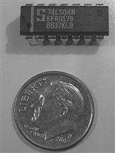
74LS04 inverter chip in a 14-pin dual inline package. The part number is on the first line. LS indicates the logic family (see Section A.6). The N suffix indicates a DIP package. The large S is the logo of the manufacturer, Signetics. The bottom two lines of gibberish are codes indicating the batch in which the chip was manufactured.
A.2.1 Logic Gates
Figure A.1 shows the pinout diagrams for a variety of popular 74xx-series chips containing basic logic gates. These are sometimes called small-scale integration (SSI) chips, because they are built from a few transistors. The 14-pin packages typically have a notch at the top or a dot on the top left to indicate orientation. Pins are numbered starting with 1 in the upper left and going counterclockwise around the package. The chips need to receive power (VDD = 5 V) and ground (GND = 0 V) at pins 14 and 7, respectively. The number of logic gates on the chip is determined by the number of pins. Note that pins 3 and 11 of the 7421 chip are not connected (NC) to anything. The 7474 flip-flop has the usual D, CLK, and Q terminals. It also has a complementary output, ![]() Moreover, it receives asynchronous set (also called preset, or PRE) and reset (also called clear, or CLR) signals. These are active low; in other words, the flop sets when
Moreover, it receives asynchronous set (also called preset, or PRE) and reset (also called clear, or CLR) signals. These are active low; in other words, the flop sets when ![]() resets when
resets when ![]() and operates normally when
and operates normally when ![]()
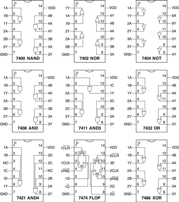
Figure A.1 Common 74xx-series logic gates
A.2.2 Other Functions
The 74xx series also includes somewhat more complex logic functions, including those shown in Figures A.2 and A.3. These are called medium-scale integration (MSI) chips. Most use larger packages to accommodate more inputs and outputs. Power and ground are still provided at the upper right and lower left, respectively, of each chip. A general functional description is provided for each chip. See the manufacturer’s data sheets for complete descriptions.
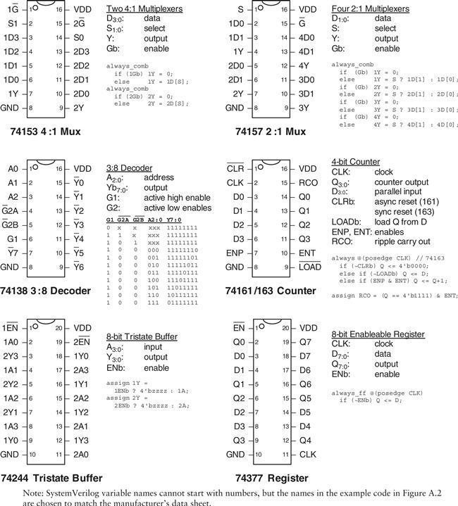
Figure A.2 Medium-scale integration chips
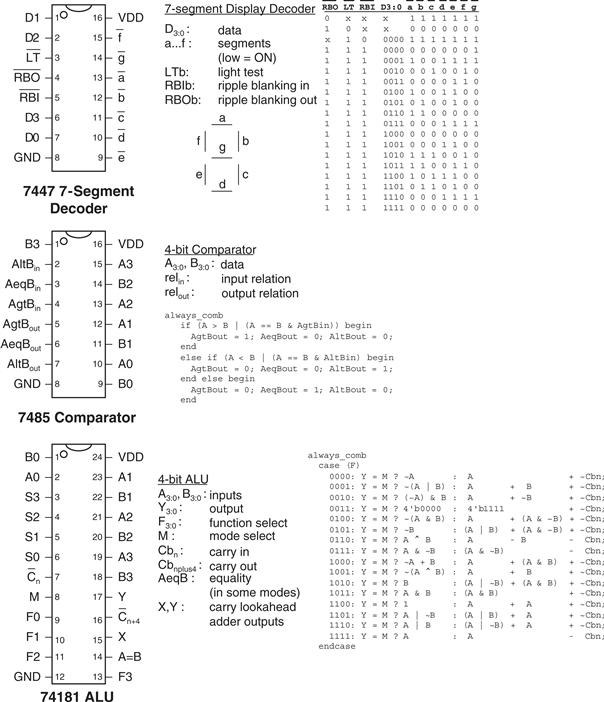
Figure A.3 More medium-scale integration (MSI) chips
A.3 Programmable Logic
Programmable logic consists of arrays of circuitry that can be configured to perform specific logic functions. We have already introduced three forms of programmable logic: programmable read only memories (PROMs), programmable logic arrays (PLAs), and field programmable gate arrays (FPGAs). This section shows chip implementations for each of these. Configuration of these chips may be performed by blowing on-chip fuses to connect or disconnect circuit elements. This is called one-time programmable (OTP) logic because, once a fuse is blown, it cannot be restored. Alternatively, the configuration may be stored in a memory that can be reprogrammed at will. Reprogrammable logic is convenient in the laboratory because the same chip can be reused during development.
A.3.1 PROMs
As discussed in Section 5.5.7, PROMs can be used as lookup tables. A 2N-word × M-bit PROM can be programmed to perform any combinational function of N inputs and M outputs. Design changes simply involve replacing the contents of the PROM rather than rewiring connections between chips. Lookup tables are useful for small functions but become prohibitively expensive as the number of inputs grows.
For example, the classic 2764 8-KB (64-Kb) erasable PROM (EPROM) is shown in Figure A.4. The EPROM has 13 address lines to specify one of the 8K words and 8 data lines to read the byte of data at that word. The chip enable and output enable must both be asserted for data to be read. The maximum propagation delay is 200 ps. In normal operation, ![]() and VPP is not used. The EPROM is usually programmed on a special programmer that sets
and VPP is not used. The EPROM is usually programmed on a special programmer that sets ![]() applies 13 V to VPP, and uses a special sequence of inputs to configure the memory.
applies 13 V to VPP, and uses a special sequence of inputs to configure the memory.
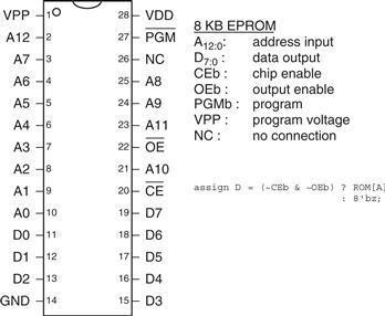
Figure A.4 2764 8KB EPROM
Modern PROMs are similar in concept but have much larger capacities and more pins. Flash memory is the cheapest type of PROM, selling for about $1 per gigabyte in 2012. Prices have historically declined by 30 to 40% per year.
A.3.2 PLAs
As discussed in Section 5.6.1, PLAs contain AND and OR planes to compute any combinational function written in sum-of-products form. The AND and OR planes can be programmed using the same techniques for PROMs. A PLA has two columns for each input and one column for each output. It has one row for each minterm. This organization is more efficient than a PROM for many functions, but the array still grows excessively large for functions with numerous I/Os and minterms.
Many different manufacturers have extended the basic PLA concept to build programmable logic devices (PLDs) that include registers. The 22V10 is one of the most popular classic PLDs. It has 12 dedicated input pins and 10 outputs. The outputs can come directly from the PLA or from clocked registers on the chip. The outputs can also be fed back into the PLA. Thus, the 22V10 can directly implement FSMs with up to 12 inputs, 10 outputs, and 10 bits of state. The 22V10 costs about $2 in quantities of 100. PLDs have been rendered mostly obsolete by the rapid improvements in capacity and cost of FPGAs.
A.3.3 FPGAs
As discussed in Section 5.6.2, FPGAs consist of arrays of configurable logic elements (LEs), also called configurable logic blocks (CLBs), connected together with programmable wires. The LEs contain small lookup tables and flip-flops. FPGAs scale gracefully to extremely large capacities, with thousands of lookup tables. Xilinx and Altera are two of the leading FPGA manufacturers.
Lookup tables and programmable wires are flexible enough to implement any logic function. However, they are an order of magnitude less efficient in speed and cost (chip area) than hard-wired versions of the same functions. Thus, FPGAs often include specialized blocks, such as memories, multipliers, and even entire microprocessors.
Figure A.5 shows the design process for a digital system on an FPGA. The design is usually specified with a hardware description language (HDL), although some FPGA tools also support schematics. The design is then simulated. Inputs are applied and compared against expected outputs to verify that the logic is correct. Usually some debugging is required. Next, logic synthesis converts the HDL into Boolean functions. Good synthesis tools produce a schematic of the functions, and the prudent designer examines these schematics, as well as any warnings produced during synthesis, to ensure that the desired logic was produced. Sometimes sloppy coding leads to circuits that are much larger than intended or to circuits with asynchronous logic. When the synthesis results are good, the FPGA tool maps the functions onto the LEs of a specific chip. The place and route tool determines which functions go in which lookup tables and how they are wired together. Wire delay increases with length, so critical circuits should be placed close together. If the design is too big to fit on the chip, it must be reengineered. Timing analysis compares the timing constraints (e.g., an intended clock speed of 100 MHz) against the actual circuit delays and reports any errors. If the logic is too slow, it may have to be redesigned or pipelined differently. When the design is correct, a file is generated specifying the contents of all the LEs and the programming of all the wires on the FPGA. Many FPGAs store this configuration information in static RAM that must be reloaded each time the FPGA is turned on. The FPGA can download this information from a computer in the laboratory, or can read it from a nonvolatile ROM when power is first applied.
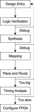
Figure A.5 FPGA design flow
Example A.1 FPGA Timing Analysis
Alyssa P. Hacker is using an FPGA to implement an M&M sorter with a color sensor and motors to put red candy in one jar and green candy in another. Her design is implemented as an FSM, and she is using a Cyclone IV GX. According to the data sheet, the FPGA has the timing characteristics shown in Table A.1.
Table A.1 Cyclone IV GX timing
| name | value (ps) |
| tpcq | 199 |
| tsetup | 76 |
| thold | 0 |
| tpd (per LE) | 381 |
| twire (between LEs) | 246 |
| tskew | 0 |
Alyssa would like her FSM to run at 100 MHz. What is the maximum number of LEs on the critical path? What is the fastest speed at which her FSM could possibly run?
Solution
At 100 MHz, the cycle time, Tc, is 10 ns. Alyssa uses Equation 3.13 to figure out the minimum combinational propagation delay, tpd, at this cycle time:
![]() (A.1)
(A.1)
With a combined LE and wire delay of 381 ps + 246 ps = 627 ps, Alyssa’s FSM can use at most 15 consecutive LEs (9.725/0.627) to implement the next-state logic.
The fastest speed at which an FSM will run on this Cyclone IV FPGA is when it is using a single LE for the next state logic. The minimum cycle time is
![]() (A.2)
(A.2)
Therefore, the maximum frequency is 1.5 GHz.
Altera advertises the Cyclone IV FPGA with 14,400 LEs for $25 in 2012. In large quantities, medium-sized FPGAs typically cost several dollars. The largest FPGAs cost hundreds or even thousands of dollars. The cost has declined at approximately 30% per year, so FPGAs are becoming extremely popular.
A.4 Application-Specific Integrated Circuits
Application-specific integrated circuits (ASICs) are chips designed for a particular purpose. Graphics accelerators, network interface chips, and cell phone chips are common examples of ASICS. The ASIC designer places transistors to form logic gates and wires the gates together. Because the ASIC is hardwired for a specific function, it is typically several times faster than an FPGA and occupies an order of magnitude less chip area (and hence cost) than an FPGA with the same function. However, the masks specifying where transistors and wires are located on the chip cost hundreds of thousands of dollars to produce. The fabrication process usually requires 6 to 12 weeks to manufacture, package, and test the ASICs. If errors are discovered after the ASIC is manufactured, the designer must correct the problem, generate new masks, and wait for another batch of chips to be fabricated. Hence, ASICs are suitable only for products that will be produced in large quantities and whose function is well defined in advance.
Figure A.6 shows the ASIC design process, which is similar to the FPGA design process of Figure A.5. Logic verification is especially important because correction of errors after the masks are produced is expensive. Synthesis produces a netlist consisting of logic gates and connections between the gates; the gates in this netlist are placed, and the wires are routed between gates. When the design is satisfactory, masks are generated and used to fabricate the ASIC. A single speck of dust can ruin an ASIC, so the chips must be tested after fabrication. The fraction of manufactured chips that work is called the yield; it is typically 50 to 90%, depending on the size of the chip and the maturity of the manufacturing process. Finally, the working chips are placed in packages, as will be discussed in Section A.7.
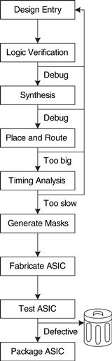
Figure A.6 ASIC design flow
A.5 Data Sheets
Integrated circuit manufacturers publish data sheets that describe the functions and performance of their chips. It is essential to read and understand the data sheets. One of the leading sources of errors in digital systems comes from misunderstanding the operation of a chip.
Data sheets are usually available from the manufacturer’s Web site. If you cannot locate the data sheet for a part and do not have clear documentation from another source, don’t use the part. Some of the entries in the data sheet may be cryptic. Often the manufacturer publishes data books containing data sheets for many related parts. The beginning of the data book has additional explanatory information. This information can usually be found on the Web with a careful search.
This section dissects the Texas Instruments (TI) data sheet for a 74HC04 inverter chip. The data sheet is relatively simple but illustrates many of the major elements. TI still manufacturers a wide variety of 74xx-series chips. In the past, many other companies built these chips too, but the market is consolidating as the sales decline.
Figure A.7 shows the first page of the data sheet. Some of the key sections are highlighted in blue. The title is SN54HC04, SN74HC04 HEX INVERTERS. HEX INVERTERS means that the chip contains six inverters. SN indicates that TI is the manufacturer. Other manufacture codes include MC for Motorola and DM for National Semiconductor. You can generally ignore these codes, because all of the manufacturers build compatible 74xx-series logic. HC is the logic family (high speed CMOS). The logic family determines the speed and power consumption of the chip, but not the function. For example, the 7404, 74HC04, and 74LS04 chips all contain six inverters, but they differ in performance and cost. Other logic families are discussed in Section A.6. The 74xx chips operate across the commercial or industrial temperature range (0 to 70 °C or −40 to 85 °C, respectively), whereas the 54xx chips operate across the military temperature range (−55 to 125 °C) and sell for a higher price but are otherwise compatible.
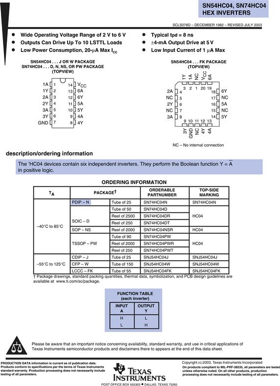
Figure A.7 7404 data sheet page 1
The 7404 is available in many different packages, and it is important to order the one you intended when you make a purchase. The packages are distinguished by a suffix on the part number. N indicates a plastic dual inline package (PDIP), which fits in a breadboard or can be soldered in through-holes in a printed circuit board. Other packages are discussed in Section A.7.
The function table shows that each gate inverts its input. If A is HIGH (H), Y is LOW (L) and vice versa. The table is trivial in this case but is more interesting for more complex chips.
Figure A.8 shows the second page of the data sheet. The logic diagram indicates that the chip contains inverters. The absolute maximum section indicates conditions beyond which the chip could be destroyed. In particular, the power supply voltage (VCC, also called VDD in this book) should not exceed 7 V. The continuous output current should not exceed 25 mA. The thermal resistance or impedance, θJA, is used to calculate the temperature rise caused by the chip’s dissipating power. If the ambient temperature in the vicinity of the chip is TA and the chip dissipates Pchip, then the temperature on the chip itself at its junction with the package is
![]() (A.3)
(A.3)
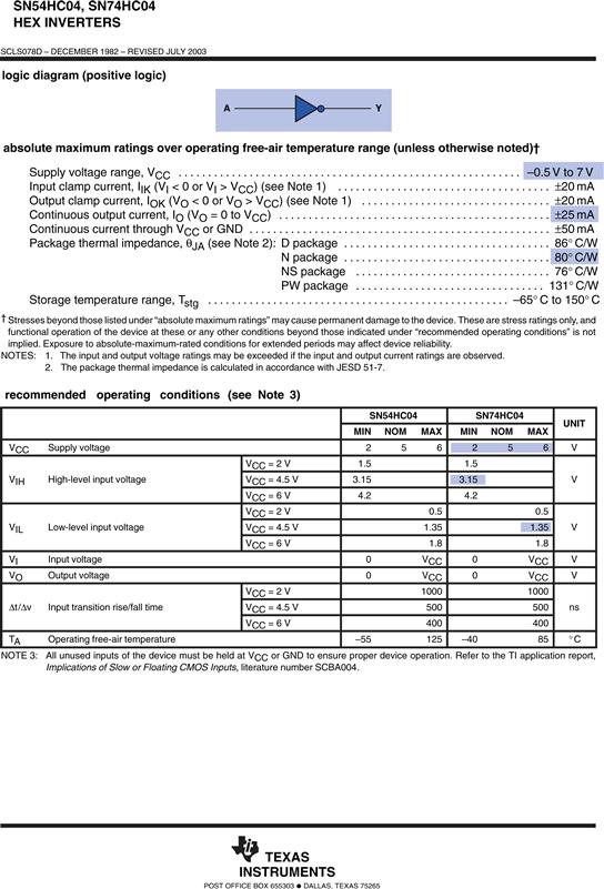
Figure A.8 7404 data sheet page 2
For example, if a 7404 chip in a plastic DIP package is operating in a hot box at 50 °C and consumes 20 mW, the junction temperature will climb to 50 °C + 0.02 W × 80 °C/W = 51.6 °C. Internal power dissipation is seldom important for 74xx-series chips, but it becomes important for modern chips that dissipate tens of watts or more.
The recommended operating conditions define the environment in which the chip should be used. Within these conditions, the chip should meet specifications. These conditions are more stringent than the absolute maximums. For example, the power supply voltage should be between 2 and 6 V. The input logic levels for the HC logic family depend on VDD. Use the 4.5 V entries when VDD = 5 V, to allow for a 10% droop in the power supply caused by noise in the system.
Figure A.9 shows the third page of the data sheet. The electrical characteristics describe how the device performs when used within the recommended operating conditions if the inputs are held constant. For example, if VCC = 5 V (and droops to 4.5 V) and the output current IOH/IOL does not exceed 20 μΑ, VOH = 4.4 V and VOL = 0.1 V in the worst case. If the output current increases, the output voltages become less ideal, because the transistors on the chip struggle to provide the current. The HC logic family uses CMOS transistors that draw very little current. The current into each input is guaranteed to be less than 1000 nA and is typically only 0.1 nA at room temperature. The quiescent power supply current (IDD) drawn while the chip is idle is less than 20 μΑ. Each input has less than 10 pF of capacitance.
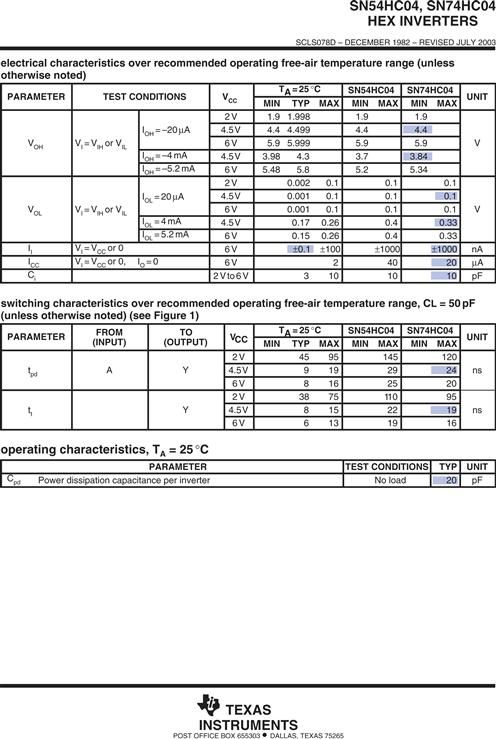
Figure A.9 7404 data sheet page 3
The switching characteristics define how the device performs when used within the recommended operating conditions if the inputs change. The propagation delay, tpd, is measured from when the input passes through 0.5 VCC to when the output passes through 0.5 VCC. If VCC is nominally 5 V and the chip drives a capacitance of less than 50 pF, the propagation delay will not exceed 24 ns (and typically will be much faster). Recall that each input may present 10 pF, so the chip cannot drive more than five identical chips at full speed. Indeed, stray capacitance from the wires connecting chips cuts further into the useful load. The transition time, also called the rise/fall time, is measured as the output transitions between 0.1 VCC and 0.9 VCC.
Recall from Section 1.8 that chips consume both static and dynamic power. Static power is low for HC circuits. At 85 °C, the maximum quiescent supply current is 20 μΑ. At 5 V, this gives a static power consumption of 0.1 mW. The dynamic power depends on the capacitance being driven and the switching frequency. The 7404 has an internal power dissipation capacitance of 20 pF per inverter. If all six inverters on the 7404 switch at 10 MHz and drive external loads of 25 pF, then the dynamic power given by Equation 1.4 is ![]() (6)(20 pF + 25 pF)(52)(10 MHz) = 33.75 mW and the maximum total power is 33.85 mW.
(6)(20 pF + 25 pF)(52)(10 MHz) = 33.75 mW and the maximum total power is 33.85 mW.
A.6 Logic Families
The 74xx-series logic chips have been manufactured using many different technologies, called logic families, that offer different speed, power, and logic level trade-offs. Other chips are usually designed to be compatible with some of these logic families. The original chips, such as the 7404, were built using bipolar transistors in a technology called Transistor-Transistor Logic (TTL). Newer technologies add one or more letters after the 74 to indicate the logic family, such as 74LS04, 74HC04, or 74AHCT04. Table A.2 summarizes the most common 5-V logic families.
Advances in bipolar circuits and process technology led to the Schottky (S) and Low-Power Schottky (LS) families. Both are faster than TTL. Schottky draws more power, whereas Low-Power Schottky draws less. Advanced Schottky (AS) and Advanced Low-Power Schottky (ALS) have improved speed and power compared to S and LS. Fast (F) logic is faster and draws less power than AS. All of these families provide more current for LOW outputs than for HIGH outputs and hence have asymmetric logic levels. They conform to the “TTL” logic levels: VIH = 2 V, VIL = 0.8 V, VOH > 2.4 V, and VOL < 0.5 V.
Table A.2 Typical specifications for 5-V logic families
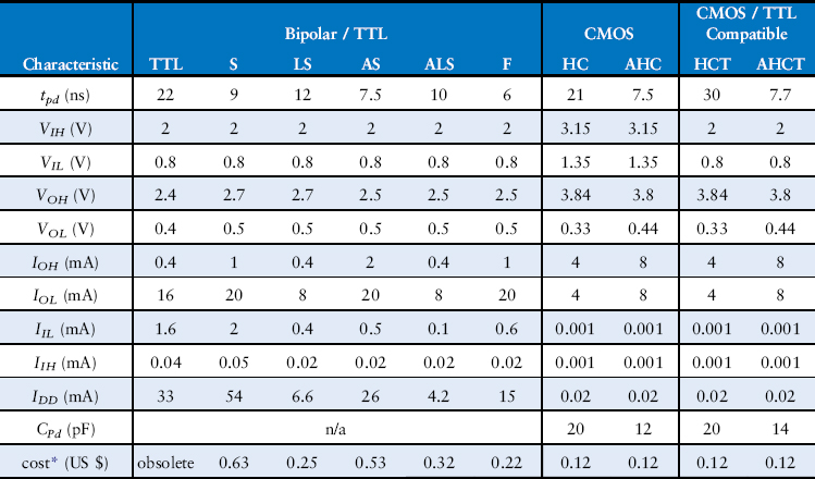
* Per unit in quantities of 1000 for the 7408 from Texas Instruments in 2012
As CMOS circuits matured in the 1980s and 1990s, they became popular because they draw very little power supply or input current. The High Speed CMOS (HC) and Advanced High Speed CMOS (AHC) families draw almost no static power. They also deliver the same current for HIGH and LOW outputs. They conform to the “CMOS” logic levels: VIH = 3.15 V, VIL = 1.35 V, VOH > 3.8 V, and VOL < 0.44 V. Unfortunately, these levels are incompatible with TTL circuits, because a TTL HIGH output of 2.4 V may not be recognized as a legal CMOS HIGH input. This motivates the use of High Speed TTL-compatible CMOS (HCT) and Advanced High Speed TTL-compatible CMOS (AHCT), which accept TTL input logic levels and generate valid CMOS output logic levels. These families are slightly slower than their pure CMOS counterparts. All CMOS chips are sensitive to electrostatic discharge (ESD) caused by static electricity. Ground yourself by touching a large metal object before handling CMOS chips, lest you zap them.
The 74xx-series logic is inexpensive. The newer logic families are often cheaper than the obsolete ones. The LS family is widely available and robust and is a popular choice for laboratory or hobby projects that have no special performance requirements.
The 5-V standard collapsed in the mid-1990s, when transistors became too small to withstand the voltage. Moreover, lower voltage offers lower power consumption. Now 3.3, 2.5, 1.8, 1.2, and even lower voltages are commonly used. The plethora of voltages raises challenges in communicating between chips with different power supplies. Table A.3 lists some of the low-voltage logic families. Not all 74xx parts are available in all of these logic families.
Table A.3 Typical specifications for low-voltage logic families
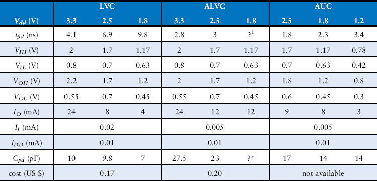
* Delay and capacitance not available at the time of writing
All of the low-voltage logic families use CMOS transistors, the workhorse of modern integrated circuits. They operate over a wide range of VDD, but the speed degrades at lower voltage. Low-Voltage CMOS (LVC) logic and Advanced Low-Voltage CMOS (ALVC) logic are commonly used at 3.3, 2.5, or 1.8 V. LVC withstands inputs up to 5.5 V, so it can receive inputs from 5-V CMOS or TTL circuits. Advanced Ultra-Low-Voltage CMOS (AUC) is commonly used at 2.5, 1.8, or 1.2 V and is exceptionally fast. Both ALVC and AUC withstand inputs up to 3.6 V, so they can receive inputs from 3.3-V circuits.
FPGAs often offer separate voltage supplies for the internal logic, called the core, and for the input/output (I/O) pins. As FPGAs have advanced, the core voltage has dropped from 5 to 3.3, 2.5, 1.8, and 1.2 V to save power and avoid damaging the very small transistors. FPGAs have configurable I/Os that can operate at many different voltages, so as to be compatible with the rest of the system.
A.7 Packaging and Assembly
Integrated circuits are typically placed in packages made of plastic or ceramic. The packages serve a number of functions, including connecting the tiny metal I/O pads of the chip to larger pins in the package for ease of connection, protecting the chip from physical damage, and spreading the heat generated by the chip over a larger area to help with cooling. The packages are placed on a breadboard or printed circuit board and wired together to assemble the system.
Packages
Figure A.10 shows a variety of integrated circuit packages. Packages can be generally categorized as through-hole or surface mount (SMT). Through-hole packages, as their name implies, have pins that can be inserted through holes in a printed circuit board or into a socket. Dual inline packages (DIPs) have two rows of pins with 0.1-inch spacing between pins. Pin grid arrays (PGAs) support more pins in a smaller package by placing the pins under the package. SMT packages are soldered directly to the surface of a printed circuit board without using holes. Pins on SMT parts are called leads. The thin small outline package (TSOP) has two rows of closely spaced leads (typically 0.02-inch spacing). Plastic leaded chip carriers (PLCCs) have J-shaped leads on all four sides, with 0.05-inch spacing. They can be soldered directly to a board or placed in special sockets. Quad flat packs (QFPs) accommodate a large number of pins using closely spaced legs on all four sides. Ball grid arrays (BGAs) eliminate the legs altogether. Instead, they have hundreds of tiny solder balls on the underside of the package. They are carefully placed over matching pads on a printed circuit board, then heated so that the solder melts and joins the package to the underlying board.
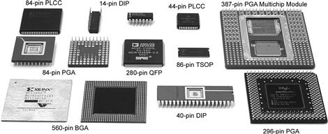
Figure A.10 Integrated circuit packages
Breadboards
DIPs are easy to use for prototyping, because they can be placed in a breadboard. A breadboard is a plastic board containing rows of sockets, as shown in Figure A.11. All five holes in a row are connected together. Each pin of the package is placed in a hole in a separate row. Wires can be placed in adjacent holes in the same row to make connections to the pin. Breadboards often provide separate columns of connected holes running the height of the board to distribute power and ground.

Figure A.11 Majority circuit on breadboard
Figure A.11 shows a breadboard containing a majority gate built with a 74LS08 AND chip and a 74LS32 OR chip. The schematic of the circuit is shown in Figure A.12. Each gate in the schematic is labeled with the chip (08 or 32) and the pin numbers of the inputs and outputs (see Figure A.1). Observe that the same connections are made on the breadboard. The inputs are connected to pins 1, 2, and 5 of the 08 chip, and the output is measured at pin 6 of the 32 chip. Power and ground are connected to pins 14 and 7, respectively, of each chip, from the vertical power and ground columns that are attached to the banana plug receptacles, Vb and Va. Labeling the schematic in this way and checking off connections as they are made is a good way to reduce the number of mistakes made during breadboarding.
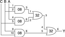
Figure A.12 Majority gate schematic with chips and pins identified
Unfortunately, it is easy to accidentally plug a wire in the wrong hole or have a wire fall out, so breadboarding requires a great deal of care (and usually some debugging in the laboratory). Breadboards are suited only to prototyping, not production.
Printed Circuit Boards
Instead of breadboarding, chip packages may be soldered to a printed circuit board (PCB). The PCB is formed of alternating layers of conducting copper and insulating epoxy. The copper is etched to form wires called traces. Holes called vias are drilled through the board and plated with metal to connect between layers. PCBs are usually designed with computer-aided design (CAD) tools. You can etch and drill your own simple boards in the laboratory, or you can send the board design to a specialized factory for inexpensive mass production. Factories have turnaround times of days (or weeks, for cheap mass production runs) and typically charge a few hundred dollars in setup fees and a few dollars per board for moderately complex boards built in large quantities.
PCB traces are normally made of copper because of its low resistance. The traces are embedded in an insulating material, usually a green, fire-resistant plastic called FR4. A PCB also typically has copper power and ground layers, called planes, between signal layers. Figure A.13 shows a cross-section of a PCB. The signal layers are on the top and bottom, and the power and ground planes are embedded in the center of the board. The power and ground planes have low resistance, so they distribute stable power to components on the board. They also make the capacitance and inductance of the traces uniform and predictable.

Figure A.13 Printed circuit board cross-section
Figure A.14 shows a PCB for a 1970s vintage Apple II+ computer. At the top is a 6502 microprocessor. Beneath are six 16-Kb ROM chips forming 12 KB of ROM containing the operating system. Three rows of eight 16-Kb DRAM chips provide 48 KB of RAM. On the right are several rows of 74xx-series logic for memory address decoding and other functions. The lines between chips are traces that wire the chips together. The dots at the ends of some of the traces are vias filled with metal.
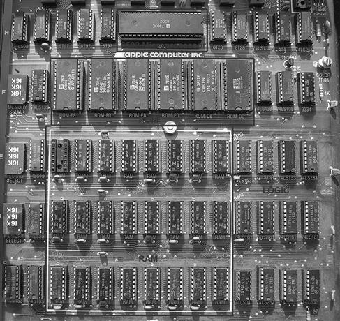
Figure A.14 Apple II+ circuit board
Putting It All Together
Most modern chips with large numbers of inputs and outputs use SMT packages, especially QFPs and BGAs. These packages require a printed circuit board rather than a breadboard. Working with BGAs is especially challenging because they require specialized assembly equipment. Moreover, the balls cannot be probed with a voltmeter or oscilloscope during debugging in the laboratory, because they are hidden under the package.
In summary, the designer needs to consider packaging early on to determine whether a breadboard can be used during prototyping and whether BGA parts will be required. Professional engineers rarely use breadboards when they are confident of connecting chips together correctly without experimentation.
A.8 Transmission Lines
We have assumed so far that wires are equipotential connections that have a single voltage along their entire length. Signals actually propagate along wires at the speed of light in the form of electromagnetic waves. If the wires are short enough or the signals change slowly, the equipotential assumption is good enough. When the wire is long or the signal is very fast, the transmission time along the wire becomes important to accurately determine the circuit delay. We must model such wires as transmission lines, in which a wave of voltage and current propagates at the speed of light. When the wave reaches the end of the line, it may reflect back along the line. The reflection may cause noise and odd behaviors unless steps are taken to limit it. Hence, the digital designer must consider transmission line behavior to accurately account for the delay and noise effects in long wires.
Electromagnetic waves travel at the speed of light in a given medium, which is fast but not instantaneous. The speed of light, ν, depends on the permittivity, ε, and permeability, μ, of the medium1: ![]()
The speed of light in free space is v = c = 3 × 10⁸ m/s. Signals in a PCB travel at about half this speed, because the FR4 insulator has four times the permittivity of air. Thus, PCB signals travel at about 1.5 × 10⁸ m/s, or 15 cm/ns. The time delay for a signal to travel along a transmission line of length l is
![]() (A.4)
(A.4)
The characteristic impedance of a transmission line, Z0 (pronounced “Z-naught”), is the ratio of voltage to current in a wave traveling along the line: Z0 = V/I. It is not the resistance of the wire (a good transmission line in a digital system typically has negligible resistance). Z0 depends on the inductance and capacitance of the line (see the derivation in Section A.8.7) and typically has a value of 50 to 75 Ω.
![]() (A.5)
(A.5)
Figure A.15 shows the symbol for a transmission line. The symbol resembles a coaxial cable with an inner signal conductor and an outer grounded conductor like that used in television cable wiring.
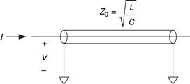
Figure A.15 Transmission line symbol
The key to understanding the behavior of transmission lines is to visualize the wave of voltage propagating along the line at the speed of light. When the wave reaches the end of the line, it may be absorbed or reflected, depending on the termination or load at the end. Reflections travel back along the line, adding to the voltage already on the line. Terminations are classified as matched, open, short, or mismatched. The following sections explore how a wave propagates along the line and what happens to the wave when it reaches the termination.
A.8.1 Matched Termination
Figure A.16 shows a transmission line of length l with a matched termination, which means that the load impedance, ZL, is equal to the characteristic impedance, Z0. The transmission line has a characteristic impedance of 50 Ω. One end of the line is connected to a voltage source through a switch that closes at time t = 0. The other end is connected to the 50 Ω matched load. This section analyzes the voltages and currents at points A, B, and C—at the beginning of the line, one-third of the length along the line, and at the end of the line, respectively.
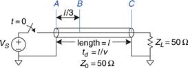
Figure A.16 Transmission line with matched termination
Figure A.17 shows the voltages at points A, B, and C over time. Initially, there is no voltage or current flowing in the transmission line, because the switch is open. At time t = 0, the switch closes, and the voltage source launches a wave with voltage V = VS along the line. This is called the incident wave. Because the characteristic impedance is Z0, the wave has current I = VS/Z0. The voltage reaches the beginning of the line (point A) immediately, as shown in Figure A.17(a). The wave propagates along the line at the speed of light. At time td/3, the wave reaches point B. The voltage at this point abruptly rises from 0 to VS, as shown in Figure A.17(b). At time td, the incident wave reaches point C at the end of the line, and the voltage rises there too. All of the current, I, flows into the resistor, ZL, producing a voltage across the resistor of ZLI = ZL (VS/Z0) = VS because ZL = Z0. This voltage is consistent with the wave flowing along the transmission line. Thus, the wave is absorbed by the load impedance, and the transmission line reaches its steady state.
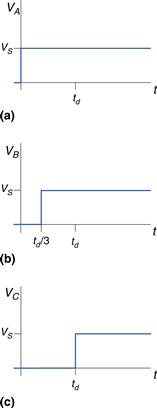
Figure A.17 Voltage waveforms for Figure A.16 at points A, B, and C
In steady state, the transmission line behaves like an ideal equipotential wire because it is, after all, just a wire. The voltage at all points along the line must be identical. Figure A.18 shows the steady-state equivalent model of the circuit in Figure A.16. The voltage is VS everywhere along the wire.
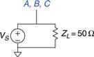
Figure A.18 Equivalent circuit of Figure A.16 at steady state
Example A.2 Transmission Line with Matched Source and Load Terminations
Figure A.19 shows a transmission line with matched source and load impedances ZS and ZL. Plot the voltage at nodes A, B, and C versus time. When does the system reach steady-state, and what is the equivalent circuit at steady-state?
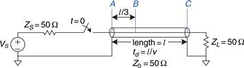
Figure A.19 Transmission line with matched source and load impedances
Solution
When the voltage source has a source impedance ZS in series with the transmission line, part of the voltage drops across ZS, and the remainder propagates down the transmission line. At first, the transmission line behaves as an impedance Z0, because the load at the end of the line cannot possibly influence the behavior of the line until a speed of light delay has elapsed. Hence, by the voltage divider equation, the incident voltage flowing down the line is
![]() (A.6)
(A.6)
Thus, at t = 0, a wave of voltage, ![]() is sent down the line from point A. Again, the signal reaches point B at time td/3 and point C at td, as shown in Figure A.20. All of the current is absorbed by the load impedance ZL, so the circuit enters steady-state at t = td. In steady-state, the entire line is at VS/2, just as the steady-state equivalent circuit in Figure A.21 would predict.
is sent down the line from point A. Again, the signal reaches point B at time td/3 and point C at td, as shown in Figure A.20. All of the current is absorbed by the load impedance ZL, so the circuit enters steady-state at t = td. In steady-state, the entire line is at VS/2, just as the steady-state equivalent circuit in Figure A.21 would predict.
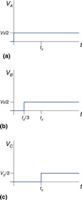
Figure A.20 Voltage waveforms for Figure A.19 at points A, B, and C
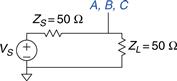
Figure A.21 Equivalent circuit of Figure A.19 at steady state
A.8.2 Open Termination
When the load impedance is not equal to Z0, the termination cannot absorb all of the current, and some of the wave must be reflected. Figure A.22 shows a transmission line with an open load termination. No current can flow through an open termination, so the current at point C must always be 0.
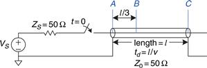
Figure A.22 Transmission line with open load termination
The voltage on the line is initially zero. At t = 0, the switch closes and a wave of voltage, ![]() begins propagating down the line. Notice that this initial wave is the same as that of Example A.2 and is independent of the termination, because the load at the end of the line cannot influence the behavior at the beginning until at least 2td has elapsed. This wave reaches point B at td/3 and point C at td as shown in Figure A.23.
begins propagating down the line. Notice that this initial wave is the same as that of Example A.2 and is independent of the termination, because the load at the end of the line cannot influence the behavior at the beginning until at least 2td has elapsed. This wave reaches point B at td/3 and point C at td as shown in Figure A.23.
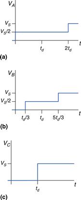
Figure A.23 Voltage waveforms for Figure A.22 at points A, B, and C
When the incident wave reaches point C, it cannot continue forward because the wire is open. It must instead reflect back toward the source. The reflected wave also has voltage ![]() because the open termination reflects the entire wave.
because the open termination reflects the entire wave.
The voltage at any point is the sum of the incident and reflected waves. At time t = td, the voltage at point C is ![]() The reflected wave reaches point B at 5td/3 and point A at 2td. When it reaches point A, the wave is absorbed by the source termination impedance that matches the characteristic impedance of the line. Thus, the system reaches steady state at time t = 2td, and the transmission line becomes equivalent to an equipotential wire with voltage VS and current I = 0.
The reflected wave reaches point B at 5td/3 and point A at 2td. When it reaches point A, the wave is absorbed by the source termination impedance that matches the characteristic impedance of the line. Thus, the system reaches steady state at time t = 2td, and the transmission line becomes equivalent to an equipotential wire with voltage VS and current I = 0.
A.8.3 Short Termination
Figure A.24 shows a transmission line terminated with a short circuit to ground. Thus, the voltage at point C must always be 0.

Figure A.24 Transmission line with short termination
As in the previous examples, the voltages on the line are initially 0. When the switch closes, a wave of voltage, ![]() begins propagating down the line (Figure A.25). When it reaches the end of the line, it must reflect with opposite polarity. The reflected wave, with voltage
begins propagating down the line (Figure A.25). When it reaches the end of the line, it must reflect with opposite polarity. The reflected wave, with voltage ![]() adds to the incident wave, ensuring that the voltage at point C remains 0. The reflected wave reaches the source at time t = 2td and is absorbed by the source impedance. At this point, the system reaches steady state, and the transmission line is equivalent to an equipotential wire with voltage V = 0.
adds to the incident wave, ensuring that the voltage at point C remains 0. The reflected wave reaches the source at time t = 2td and is absorbed by the source impedance. At this point, the system reaches steady state, and the transmission line is equivalent to an equipotential wire with voltage V = 0.
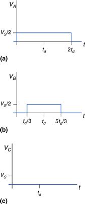
Figure A.25 Voltage waveforms for Figure A.24 at points A, B, and C
A.8.4 Mismatched Termination
The termination impedance is said to be mismatched when it does not equal the characteristic impedance of the line. In general, when an incident wave reaches a mismatched termination, part of the wave is absorbed and part is reflected. The reflection coefficient kr indicates the fraction of the incident wave Vi that is reflected: Vr = krVi.
Section A.8.8 derives the reflection coefficient using conservation of current arguments. It shows that, when an incident wave flowing along a transmission line of characteristic impedance Z0 reaches a termination impedance ZT at the end of the line, the reflection coefficient is
![]() (A.7)
(A.7)
Note a few special cases. If the termination is an open circuit (ZT = ∞), kr = 1, because the incident wave is entirely reflected (so the current out the end of the line remains zero). If the termination is a short circuit (ZT = 0), kr = –1, because the incident wave is reflected with negative polarity (so the voltage at the end of the line remains zero). If the termination is a matched load (ZT = Z0), kr = 0, because the incident wave is completely absorbed.
Figure A.26 illustrates reflections in a transmission line with a mismatched load termination of 75 Ω. ZT = ZL = 75 Ω, and Z0 = 50 Ω, so kr = 1/5. As in previous examples, the voltage on the line is initially 0. When the switch closes, a wave of voltage ![]() propagates down the line, reaching the end at t = td. When the incident wave reaches the termination at the end of the line, one fifth of the wave is reflected, and the remaining four fifths flows into the load impedance. Thus, the reflected wave has a voltage
propagates down the line, reaching the end at t = td. When the incident wave reaches the termination at the end of the line, one fifth of the wave is reflected, and the remaining four fifths flows into the load impedance. Thus, the reflected wave has a voltage ![]() The total voltage at point C is the sum of the incoming and reflected voltages,
The total voltage at point C is the sum of the incoming and reflected voltages, ![]() At t = 2td, the reflected wave reaches point A, where it is absorbed by the matched 50 Ω termination, ZS. Figure A.27 plots the voltages and currents along the line. Again, note that, in steady state (in this case at time t > 2td), the transmission line is equivalent to an equipotential wire, as shown in Figure A.28. At steady state, the system acts like a voltage divider, so
At t = 2td, the reflected wave reaches point A, where it is absorbed by the matched 50 Ω termination, ZS. Figure A.27 plots the voltages and currents along the line. Again, note that, in steady state (in this case at time t > 2td), the transmission line is equivalent to an equipotential wire, as shown in Figure A.28. At steady state, the system acts like a voltage divider, so
![]()

Figure A.26 Transmission line with mismatched termination

Figure A.27 Voltage waveforms for Figure A.26 at points A, B, and C
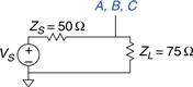
Figure A.28 Equivalent circuit of Figure A.26 at steady state
Reflections can occur at both ends of the transmission line. Figure A.29 shows a transmission line with a source impedance, ZS, of 450 Ω and an open termination at the load. The reflection coefficients at the load and source, krL and krS, are 1 and 4/5, respectively. In this case, waves reflect off both ends of the transmission line until a steady state is reached.
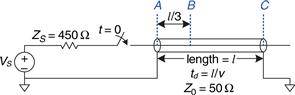
Figure A.29 Transmission line with mismatched source and load terminations
The bounce diagram shown in Figure A.30 helps visualize reflections off both ends of the transmission line. The horizontal axis represents distance along the transmission line, and the vertical axis represents time, increasing downward. The two sides of the bounce diagram represent the source and load ends of the transmission line, points A and C. The incoming and reflected signal waves are drawn as diagonal lines between points A and C. At time t = 0, the source impedance and transmission line behave as a voltage divider, launching a voltage wave of ![]() from point A toward point C. At time t = td, the signal reaches point C and is completely reflected (krL = 1). At time t = 2td, the reflected wave of
from point A toward point C. At time t = td, the signal reaches point C and is completely reflected (krL = 1). At time t = 2td, the reflected wave of ![]() reaches point A and is reflected with a reflection coefficient, krS = 4/5, to produce a wave of
reaches point A and is reflected with a reflection coefficient, krS = 4/5, to produce a wave of ![]() traveling toward point C, and so forth.
traveling toward point C, and so forth.
The voltage at a given time at any point on the transmission line is the sum of all the incident and reflected waves. Thus, at time t = 1.1td, the voltage at point C is ![]() At time t = 3.1td, the voltage at point C is
At time t = 3.1td, the voltage at point C is ![]() and so forth. Figure A.31 plots the voltages against time. As t approaches infinity, the voltages approach steady state with VA = VB = VC = VS.
and so forth. Figure A.31 plots the voltages against time. As t approaches infinity, the voltages approach steady state with VA = VB = VC = VS.
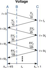
Figure A.30 Bounce diagram for Figure A.29
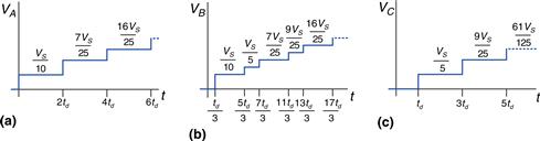
Figure A.31 Voltage and current waveforms for Figure A.29
A.8.5 When to Use Transmission Line Models
Transmission line models for wires are needed whenever the wire delay, td, is longer than a fraction (e.g., 20%) of the edge rates (rise or fall times) of a signal. If the wire delay is shorter, it has an insignificant effect on the propagation delay of the signal, and the reflections dissipate while the signal is transitioning. If the wire delay is longer, it must be considered in order to accurately predict the propagation delay and waveform of the signal. In particular, reflections may distort the digital characteristic of a waveform, resulting in incorrect logic operations.
Recall that signals travel on a PCB at about 15 cm/ns. For TTL logic, with edge rates of 10 ns, wires must be modeled as transmission lines only if they are longer than 30 cm (10 ns × 15 cm/ns × 20%). PCB traces are usually less than 30 cm, so most traces can be modeled as ideal equipotential wires. In contrast, many modern chips have edge rates of 2 ns or less, so traces longer than about 6 cm (about 2.5 inches) must be modeled as transmission lines. Clearly, use of edge rates that are crisper than necessary just causes difficulties for the designer.
Breadboards lack a ground plane, so the electromagnetic fields of each signal are nonuniform and difficult to model. Moreover, the fields interact with other signals. This can cause strange reflections and crosstalk between signals. Thus, breadboards are unreliable above a few megahertz.
In contrast, PCBs have good transmission lines with consistent characteristic impedance and velocity along the entire line. As long as they are terminated with a source or load impedance that is matched to the impedance of the line, PCB traces do not suffer from reflections.
A.8.6 Proper Transmission Line Terminations
There are two common ways to properly terminate a transmission line, shown in Figure A.32. In parallel termination, the driver has a low impedance (ZS ≈ 0). A load resistor ZL with impedance Z0 is placed in parallel with the load (between the input of the receiver gate and ground). When the driver switches from 0 to VDD, it sends a wave with voltage VDD down the line. The wave is absorbed by the matched load termination, and no reflections take place. In series termination, a source resistor ZS is placed in series with the driver to raise the source impedance to Z0. The load has a high impedance (ZL ≈ ∞). When the driver switches, it sends a wave with voltage VDD/2 down the line. The wave reflects at the open circuit load and returns, bringing the voltage on the line up to VDD. The wave is absorbed at the source termination. Both schemes are similar in that the voltage at the receiver transitions from 0 to VDD at t = td, just as one would desire. They differ in power consumption and in the waveforms that appear elsewhere along the line. Parallel termination dissipates power continuously through the load resistor when the line is at a high voltage. Series termination dissipates no DC power, because the load is an open circuit. However, in series terminated lines, points near the middle of the transmission line initially see a voltage of VDD/2, until the reflection returns. If other gates are attached to the middle of the line, they will momentarily see an illegal logic level. Therefore, series termination works best for point-to-point communication with a single driver and a single receiver. Parallel termination is better for a bus with multiple receivers, because receivers at the middle of the line never see an illegal logic level.
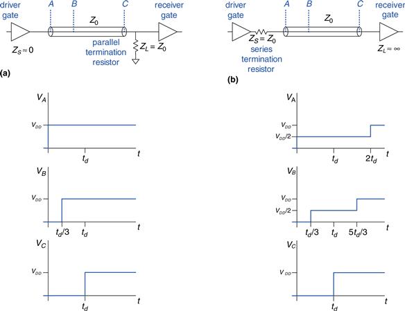
Figure A.32 Termination schemes: (a) parallel, (b) series
A.8.7 Derivation of Z0*
Z0 is the ratio of voltage to current in a wave propagating along a transmission line. This section derives Z0; it assumes some previous knowledge of resistor-inductor-capacitor (RLC) circuit analysis.
Imagine applying a step voltage to the input of a semi-infinite transmission line (so that there are no reflections). Figure A.33 shows the semi-infinite line and a model of a segment of the line of length dx. R, L, and C, are the values of resistance, inductance, and capacitance per unit length. Figure A.33(b) shows the transmission line model with a resistive component, R. This is called a lossy transmission line model, because energy is dissipated, or lost, in the resistance of the wire. However, this loss is often negligible, and we can simplify analysis by ignoring the resistive component and treating the transmission line as an ideal transmission line, as shown in Figure A.33(c).
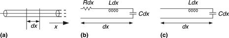
Figure A.33 Transmission line models: (a) semi-infinite cable, (b) lossy, (c) ideal
Voltage and current are functions of time and space throughout the transmission line, as given by Equations A.8 and A.9.
![]() (A.8)
(A.8)
![]() (A.9)
(A.9)
Taking the space derivative of Equation A.8 and the time derivative of Equation A.9 and substituting gives Equation A.10, the wave equation.
![]() (A.10)
(A.10)
Z0 is the ratio of voltage to current in the transmission line, as illustrated in Figure A.34(a). Z0 must be independent of the length of the line, because the behavior of the wave cannot depend on things at a distance. Because it is independent of length, the impedance must still equal Z0 after the addition of a small amount of transmission line, dx, as shown in Figure A.34(b).
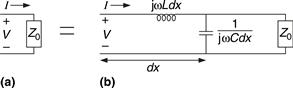
Figure A.34 Transmission line model: (a) for entire line and (b) with additional length, dx
Using the impedances of an inductor and a capacitor, we rewrite the relationship of Figure A.34 in equation form:
![]() (A.11)
(A.11)
Rearranging, we get
![]() (A.12)
(A.12)
Taking the limit as dx approaches 0, the last term vanishes and we find that
![]() (A.13)
(A.13)
A.8.8 Derivation of the Reflection Coefficient*
The reflection coefficient kr is derived using conservation of current. Figure A.35 shows a transmission line with characteristic impedance Z0 and load impedance ZL. Imagine an incident wave of voltage Vi and current Ii. When the wave reaches the termination, some current IL flows through the load impedance, causing a voltage drop VL. The remainder of the current reflects back down the line in a wave of voltage Vr and current Ir. Z0 is the ratio of voltage to current in waves propagating along the line, so ![]()
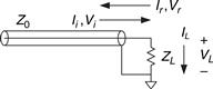
Figure A.35 Transmission line showing incoming, reflected, and load voltages and currents
The voltage on the line is the sum of the voltages of the incident and reflected waves. The current flowing in the positive direction on the line is the difference between the currents of the incident and reflected waves.
![]() (A.14)
(A.14)
![]() (A.15)
(A.15)
Using Ohm’s law and substituting for IL, Ii, and Ir in Equation A.15, we get
![]() (A.16)
(A.16)
Rearranging, we solve for the reflection coefficient, kr:
![]() (A.17)
(A.17)
A.8.9 Putting It All Together
Transmission lines model the fact that signals take time to propagate down long wires because the speed of light is finite. An ideal transmission line has uniform inductance L and capacitance C per unit length and zero resistance. The transmission line is characterized by its characteristic impedance Z0 and delay td which can be derived from the inductance, capacitance, and wire length. The transmission line has significant delay and noise effects on signals whose rise/fall times are less than about 5td. This means that, for systems with 2 ns rise/fall times, PCB traces longer than about 6 cm must be analyzed as transmission lines to accurately understand their behavior.
A digital system consisting of a gate driving a long wire attached to the input of a second gate can be modeled with a transmission line as shown in Figure A.36. The voltage source, source impedance ΖS, and switch model the first gate switching from 0 to 1 at time 0. The driver gate cannot supply infinite current; this is modeled by ZS. ZS is usually small for a logic gate, but a designer may choose to add a resistor in series with the gate to raise ZS and match the impedance of the line. The input to the second gate is modeled as ZL. CMOS circuits usually have little input current, so ZL may be close to infinity. The designer may also choose to add a resistor in parallel with the second gate, between the gate input and ground, so that ZL matches the impedance of the line.
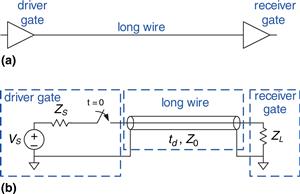
Figure A.36 Digital system modeled with transmission line
When the first gate switches, a wave of voltage is driven onto the transmission line. The source impedance and transmission line form a voltage divider, so the voltage of the incident wave is
![]() (A.18)
(A.18)
At time td, the wave reaches the end of the line. Part is absorbed by the load impedance, and part is reflected. The reflection coefficient kr indicates the portion that is reflected: kr = Vr/Vi, where Vr is the voltage of the reflected wave and Vi is the voltage of the incident wave.
![]() (A.19)
(A.19)
The reflected wave adds to the voltage already on the line. It reaches the source at time 2td, where part is absorbed and part is again reflected. The reflections continue back and forth, and the voltage on the line eventually approaches the value that would be expected if the line were a simple equipotential wire.
A.9 Economics
Although digital design is so much fun that some of us would do it for free, most designers and companies intend to make money. Therefore, economic considerations are a major factor in design decisions.
The cost of a digital system can be divided into nonrecurring engineering costs (NRE), and recurring costs. NRE accounts for the cost of designing the system. It includes the salaries of the design team, computer and software costs, and the costs of producing the first working unit. The fully loaded cost of a designer in the United States in 2012 (including salary, health insurance, retirement plan, and a computer with design tools) was roughly $200,000 per year, so design costs can be significant. Recurring costs are the cost of each additional unit; this includes components, manufacturing, marketing, technical support, and shipping.
The sales price must cover not only the cost of the system but also other costs such as office rental, taxes, and salaries of staff who do not directly contribute to the design (such as the janitor and the CEO). After all of these expenses, the company should still make a profit.
Example A.3 Ben Tries to Make Some Money
Ben Bitdiddle has designed a crafty circuit for counting raindrops. He decides to sell the device and try to make some money, but he needs help deciding what implementation to use. He decides to use either an FPGA or an ASIC. The development kit to design and test the FPGA costs $1500. Each FPGA costs $17. The ASIC costs $600,000 for a mask set and $4 per chip.
Regardless of what chip implementation he chooses, Ben needs to mount the packaged chip on a printed circuit board (PCB), which will cost him $1.50 per board. He thinks he can sell 1000 devices per month. Ben has coerced a team of bright undergraduates into designing the chip for their senior project, so it doesn’t cost him anything to design.
If the sales price has to be twice the cost (100% profit margin), and the product life is 2 years, which implementation is the better choice?
Solution
Ben figures out the total cost for each implementation over 2 years, as shown in Table A.4. Over 2 years, Ben plans on selling 24,000 devices, and the total cost is given in Table A.4 for each option. If the product life is only two years, the FPGA option is clearly superior. The per-unit cost is $445,500/24,000 = $18.56, and the sales price is $37.13 per unit to give a 100% profit margin. The ASIC option would have cost $732,000/24,000 = $30.50 and would have sold for $61 per unit.
Table A.4 ASIC vs FPGA costs
| Cost | ASIC | FPGA |
| NRE | $600,000 | $1500 |
| chip | $4 | $17 |
| PCB | $1.50 | $1.50 |
| TOTAL | $600,000 + (24,000 × $5.50) = $732,000 | $1500 + (24,000 × $18.50) = $445,500 |
| per unit | $30.50 | $18.56 |
Example A.4 Ben Gets Greedy
After seeing the marketing ads for his product, Ben thinks he can sell even more chips per month than originally expected. If he were to choose the ASIC option, how many devices per month would he have to sell to make the ASIC option more profitable than the FPGA option?
Solution
Ben solves for the minimum number of units, N, that he would need to sell in 2 years:
![]()
Solving the equation gives N = 46,039 units, or 1919 units per month. He would need to almost double his monthly sales to benefit from the ASIC solution.
Example A.5 Ben Gets Less Greedy
Ben realizes that his eyes have gotten too big for his stomach, and he doesn’t think he can sell more than 1000 devices per month. But he does think the product life can be longer than 2 years. At a sales volume of 1000 devices per month, how long would the product life have to be to make the ASIC option worthwhile?
Solution
If Ben sells more than 46,039 units in total, the ASIC option is the best choice. So, Ben would need to sell at a volume of 1000 per month for at least 47 months (rounding up), which is almost 4 years. By then, his product is likely to be obsolete.
Chips are usually purchased from a distributor rather than directly from the manufacturer (unless you are ordering tens of thousands of units). Digikey (www.digikey.com) is a leading distributor that sells a wide variety of electronics. Jameco (www.jameco.com) and All Electronics (www.allelectronics.com) have eclectic catalogs that are competitively priced and well suited to hobbyists.
1 The capacitance, C, and inductance, L, of a wire are related to the permittivity and permeability of the physical medium in which the wire is located.