
1
From Zero to One
1.1 The Game Plan
Microprocessors have revolutionized our world during the past three decades. A laptop computer today has far more capability than a room-sized mainframe of yesteryear. A luxury automobile contains about 50 microprocessors. Advances in microprocessors have made cell phones and the Internet possible, have vastly improved medicine, and have transformed how war is waged. Worldwide semiconductor industry sales have grown from US $21 billion in 1985 to $300 billion in 2011, and microprocessors are a major segment of these sales. We believe that microprocessors are not only technically, economically, and socially important, but are also an intrinsically fascinating human invention. By the time you finish reading this book, you will know how to design and build your own microprocessor. The skills you learn along the way will prepare you to design many other digital systems.
We assume that you have a basic familiarity with electricity, some prior programming experience, and a genuine interest in understanding what goes on under the hood of a computer. This book focuses on the design of digital systems, which operate on 1’s and 0’s. We begin with digital logic gates that accept 1’s and 0’s as inputs and produce 1’s and 0’s as outputs. We then explore how to combine logic gates into more complicated modules such as adders and memories. Then we shift gears to programming in assembly language, the native tongue of the microprocessor. Finally, we put gates together to build a microprocessor that runs these assembly language programs.
A great advantage of digital systems is that the building blocks are quite simple: just 1’s and 0’s. They do not require grungy mathematics or a profound knowledge of physics. Instead, the designer’s challenge is to combine these simple blocks into complicated systems. A microprocessor may be the first system that you build that is too complex to fit in your head all at once. One of the major themes weaved through this book is how to manage complexity.
1.2 The Art of Managing Complexity
One of the characteristics that separates an engineer or computer scientist from a layperson is a systematic approach to managing complexity. Modern digital systems are built from millions or billions of transistors. No human being could understand these systems by writing equations describing the movement of electrons in each transistor and solving all of the equations simultaneously. You will need to learn to manage complexity to understand how to build a microprocessor without getting mired in a morass of detail.
1.2.1 Abstraction
The critical technique for managing complexity is abstraction: hiding details when they are not important. A system can be viewed from many different levels of abstraction. For example, American politicians abstract the world into cities, counties, states, and countries. A county contains multiple cities and a state contains many counties. When a politician is running for president, the politician is mostly interested in how the state as a whole will vote, rather than how each county votes, so the state is the most useful level of abstraction. On the other hand, the Census Bureau measures the population of every city, so the agency must consider the details of a lower level of abstraction.
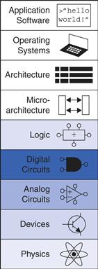
Figure 1.1 illustrates levels of abstraction for an electronic computer system along with typical building blocks at each level. At the lowest level of abstraction is the physics, the motion of electrons. The behavior of electrons is described by quantum mechanics and Maxwell’s equations. Our system is constructed from electronic devices such as transistors (or vacuum tubes, once upon a time). These devices have well-defined connection points called terminals and can be modeled by the relationship between voltage and current as measured at each terminal. By abstracting to this device level, we can ignore the individual electrons. The next level of abstraction is analog circuits, in which devices are assembled to create components such as amplifiers. Analog circuits input and output a continuous range of voltages. Digital circuits such as logic gates restrict the voltages to discrete ranges, which we will use to indicate 0 and 1. In logic design, we build more complex structures, such as adders or memories, from digital circuits.
Figure 1.1 Levels of abstraction for an electronic computing system
Microarchitecture links the logic and architecture levels of abstraction. The architecture level of abstraction describes a computer from the programmer’s perspective. For example, the Intel x86 architecture used by microprocessors in most personal computers (PCs) is defined by a set of instructions and registers (memory for temporarily storing variables) that the programmer is allowed to use. Microarchitecture involves combining logic elements to execute the instructions defined by the architecture. A particular architecture can be implemented by one of many different microarchitectures with different price/performance/power trade-offs. For example, the Intel Core i7, the Intel 80486, and the AMD Athlon all implement the x86 architecture with different microarchitectures.
Moving into the software realm, the operating system handles low-level details such as accessing a hard drive or managing memory. Finally, the application software uses these facilities provided by the operating system to solve a problem for the user. Thanks to the power of abstraction, your grandmother can surf the Web without any regard for the quantum vibrations of electrons or the organization of the memory in her computer.
This book focuses on the levels of abstraction from digital circuits through computer architecture. When you are working at one level of abstraction, it is good to know something about the levels of abstraction immediately above and below where you are working. For example, a computer scientist cannot fully optimize code without understanding the architecture for which the program is being written. A device engineer cannot make wise trade-offs in transistor design without understanding the circuits in which the transistors will be used. We hope that by the time you finish reading this book, you can pick the level of abstraction appropriate to solving your problem and evaluate the impact of your design choices on other levels of abstraction.
Each chapter in this book begins with an abstraction icon indicating the focus of the chapter in deep blue, with secondary topics shown in lighter shades of blue.
1.2.2 Discipline
Discipline is the act of intentionally restricting your design choices so that you can work more productively at a higher level of abstraction. Using interchangeable parts is a familiar application of discipline. One of the first examples of interchangeable parts was in flintlock rifle manufacturing. Until the early 19th century, rifles were individually crafted by hand. Components purchased from many different craftsmen were carefully filed and fit together by a highly skilled gunmaker. The discipline of interchangeable parts revolutionized the industry. By limiting the components to a standardized set with well-defined tolerances, rifles could be assembled and repaired much faster and with less skill. The gunmaker no longer concerned himself with lower levels of abstraction such as the specific shape of an individual barrel or gunstock.
In the context of this book, the digital discipline will be very important. Digital circuits use discrete voltages, whereas analog circuits use continuous voltages. Therefore, digital circuits are a subset of analog circuits and in some sense must be capable of less than the broader class of analog circuits. However, digital circuits are much simpler to design. By limiting ourselves to digital circuits, we can easily combine components into sophisticated systems that ultimately outperform those built from analog components in many applications. For example, digital televisions, compact disks (CDs), and cell phones are replacing their analog predecessors.
1.2.3 The Three-Y’s
In addition to abstraction and discipline, designers use the three “-y’s” to manage complexity: hierarchy, modularity, and regularity. These principles apply to both software and hardware systems.
![]() Hierarchy involves dividing a system into modules, then further subdividing each of these modules until the pieces are easy to understand.
Hierarchy involves dividing a system into modules, then further subdividing each of these modules until the pieces are easy to understand.
![]() Modularity states that the modules have well-defined functions and interfaces, so that they connect together easily without unanticipated side effects.
Modularity states that the modules have well-defined functions and interfaces, so that they connect together easily without unanticipated side effects.
![]() Regularity seeks uniformity among the modules. Common modules are reused many times, reducing the number of distinct modules that must be designed.
Regularity seeks uniformity among the modules. Common modules are reused many times, reducing the number of distinct modules that must be designed.
Captain Meriwether Lewis of the Lewis and Clark Expedition was one of the early advocates of interchangeable parts for rifles. In 1806, he explained:
The guns of Drewyer and Sergt. Pryor were both out of order. The first was repared with a new lock, the old one having become unfit for use; the second had the cock screw broken which was replaced by a duplicate which had been prepared for the lock at Harpers Ferry where she was manufactured. But for the precaution taken in bringing on those extra locks, and parts of locks, in addition to the ingenuity of John Shields, most of our guns would at this moment be entirely unfit for use; but fortunately for us I have it in my power here to record that they are all in good order.
See Elliott Coues, ed., The History of the Lewis and Clark Expedition… (4 vols), New York: Harper, 1893; reprint, 3 vols, New York: Dover, 3:817.
To illustrate these “-y’s” we return to the example of rifle manufacturing. A flintlock rifle was one of the most intricate objects in common use in the early 19th century. Using the principle of hierarchy, we can break it into components shown in Figure 1.2: the lock, stock, and barrel.
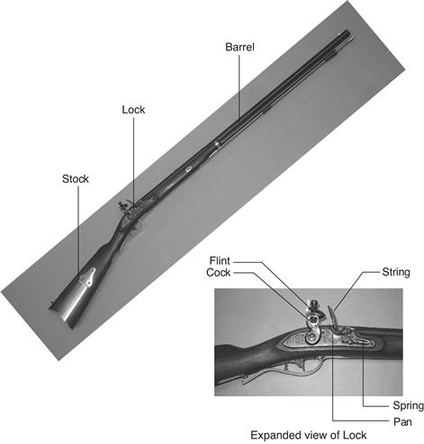
Figure 1.2 Flintlock rifle with a close-up view of the lock
Image by Euroarms Italia. www.euroarms.net © 2006.
The barrel is the long metal tube through which the bullet is fired. The lock is the firing mechanism. And the stock is the wooden body that holds the parts together and provides a secure grip for the user. In turn, the lock contains the trigger, hammer, flint, frizzen, and pan. Each of these components could be hierarchically described in further detail.
Modularity teaches that each component should have a well-defined function and interface. A function of the stock is to mount the barrel and lock. Its interface consists of its length and the location of its mounting pins. In a modular rifle design, stocks from many different manufacturers can be used with a particular barrel as long as the stock and barrel are of the correct length and have the proper mounting mechanism. A function of the barrel is to impart spin to the bullet so that it travels more accurately. Modularity dictates that there should be no side effects: the design of the stock should not impede the function of the barrel.
Regularity teaches that interchangeable parts are a good idea. With regularity, a damaged barrel can be replaced by an identical part. The barrels can be efficiently built on an assembly line, instead of being painstakingly hand-crafted.
We will return to these principles of hierarchy, modularity, and regularity throughout the book.
1.3 The Digital Abstraction
Most physical variables are continuous. For example, the voltage on a wire, the frequency of an oscillation, or the position of a mass are all continuous quantities. Digital systems, on the other hand, represent information with discrete-valued variables—that is, variables with a finite number of distinct values.
An early digital system using variables with ten discrete values was Charles Babbage’s Analytical Engine. Babbage labored from 1834 to 1871,1 designing and attempting to build this mechanical computer. The Analytical Engine used gears with ten positions labeled 0 through 9, much like a mechanical odometer in a car. Figure 1.3 shows a prototype of the Analytical Engine, in which each row processes one digit. Babbage chose 25 rows of gears, so the machine has 25-digit precision.
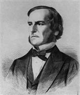
Charles Babbage, 1791–1871
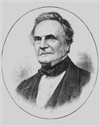
Attended Cambridge University and married Georgiana Whitmore in 1814. Invented the Analytical Engine, the world’s first mechanical computer. Also invented the cowcatcher and the universal postage rate. Interested in lock-picking, but abhorred street musicians (image courtesy of Fourmilab Switzerland, www.fourmilab.ch).
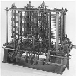
Figure 1.3 Babbage’s Analytical Engine, under construction at the time of his death in 1871
image courtesy of Science Museum/Science and Society Picture Library
Unlike Babbage’s machine, most electronic computers use a binary (two-valued) representation in which a high voltage indicates a ’1’ and a low voltage indicates a ’0’, because it is easier to distinguish between two voltages than ten.
The amount of information D in a discrete valued variable with N distinct states is measured in units of bits as
![]() (1.1)
(1.1)
A binary variable conveys log22 = 1 bit of information. Indeed, the word bit is short for binary digit. Each of Babbage’s gears carried log210 = 3.322 bits of information because it could be in one of 23.322 = 10 unique positions. A continuous signal theoretically contains an infinite amount of information because it can take on an infinite number of values. In practice, noise and measurement error limit the information to only 10 to 16 bits for most continuous signals. If the measurement must be made rapidly, the information content is lower (e.g., 8 bits).
George Boole, 1815–1864
Born to working-class parents and unable to afford a formal education, Boole taught himself mathematics and joined the faculty of Queen’s College in Ireland. He wrote An Investigation of the Laws of Thought (1854), which introduced binary variables and the three fundamental logic operations: AND, OR, and NOT (image courtesy of the American Institute of Physics).
This book focuses on digital circuits using binary variables: 1’s and 0’s. George Boole developed a system of logic operating on binary variables that is now known as Boolean logic. Each of Boole’s variables could be TRUE or FALSE. Electronic computers commonly use a positive voltage to represent ’1’ and zero volts to represent ’0’. In this book, we will use the terms ’1’, TRUE, and HIGH synonymously. Similarly, we will use ’0’, FALSE, and LOW interchangeably.
The beauty of the digital abstraction is that digital designers can focus on 1’s and 0’s, ignoring whether the Boolean variables are physically represented with specific voltages, rotating gears, or even hydraulic fluid levels. A computer programmer can work without needing to know the intimate details of the computer hardware. On the other hand, understanding the details of the hardware allows the programmer to optimize the software better for that specific computer.
An individual bit doesn’t carry much information. In the next section, we examine how groups of bits can be used to represent numbers. In later chapters, we will also use groups of bits to represent letters and programs.
1.4 Number Systems
You are accustomed to working with decimal numbers. In digital systems consisting of 1’s and 0’s, binary or hexadecimal numbers are often more convenient. This section introduces the various number systems that will be used throughout the rest of the book.
1.4.1 Decimal Numbers
In elementary school, you learned to count and do arithmetic in decimal. Just as you (probably) have ten fingers, there are ten decimal digits: 0, 1, 2, …, 9. Decimal digits are joined together to form longer decimal numbers. Each column of a decimal number has ten times the weight of the previous column. From right to left, the column weights are 1, 10, 100, 1000, and so on. Decimal numbers are referred to as base 10. The base is indicated by a subscript after the number to prevent confusion when working in more than one base. For example, Figure 1.4 shows how the decimal number 974210 is written as the sum of each of its digits multiplied by the weight of the corresponding column.
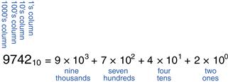
Figure 1.4 Representation of a decimal number
An N-digit decimal number represents one of 10N possibilities: 0, 1, 2, 3, …, 10N − 1. This is called the range of the number. For example, a three-digit decimal number represents one of 1000 possibilities in the range of 0 to 999.
1.4.2 Binary Numbers
Bits represent one of two values, 0 or 1, and are joined together to form binary numbers. Each column of a binary number has twice the weight of the previous column, so binary numbers are base 2. In binary, the column weights (again from right to left) are 1, 2, 4, 8, 16, 32, 64, 128, 256, 512, 1024, 2048, 4096, 8192, 16384, 32768, 65536, and so on. If you work with binary numbers often, you’ll save time if you remember these powers of two up to 216.
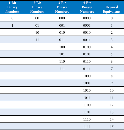
An N-bit binary number represents one of 2N possibilities: 0, 1, 2, 3, …, 2N − 1. Table 1.1 shows 1, 2, 3, and 4-bit binary numbers and their decimal equivalents.
Table 1.1 Binary numbers and their decimal equivalent
Example 1.1 Binary to Decimal Conversion
Convert the binary number 101102 to decimal.

Example 1.2 Decimal to Binary Conversion
Convert the decimal number 8410 to binary.
Solution
Determine whether each column of the binary result has a 1 or a 0. We can do this starting at either the left or the right column.
Working from the left, start with the largest power of 2 less than or equal to the number (in this case, 64). 84 ≥ 64, so there is a 1 in the 64’s column, leaving 84 − 64 = 20. 20 < 32, so there is a 0 in the 32’s column. 20 ≥ 16, so there is a 1 in the 16’s column, leaving 20 − 16 = 4. 4 < 8, so there is a 0 in the 8’s column. 4 ≥ 4, so there is a 1 in the 4’s column, leaving 4 − 4 = 0. Thus there must be 0’s in the 2’s and 1’s column. Putting this all together, 8410 = 10101002.
Working from the right, repeatedly divide the number by 2. The remainder goes in each column. 84/2 = 42, so 0 goes in the 1’s column. 42/2 = 21, so 0 goes in the 2’s column. 21/2 = 10 with a remainder of 1 going in the 4’s column. 10/2 = 5, so 0 goes in the 8’s column. 5/2 = 2 with a remainder of 1 going in the 16’s column. 2/2 = 1, so 0 goes in the 32’s column. Finally 1/2 = 0 with a remainder of 1 going in the 64’s column. Again, 8410 = 10101002.
1.4.3 Hexadecimal Numbers
Writing long binary numbers becomes tedious and prone to error. A group of four bits represents one of 24 = 16 possibilities. Hence, it is sometimes more convenient to work in base 16, called hexadecimal. Hexadecimal numbers use the digits 0 to 9 along with the letters A to F, as shown in Table 1.2. Columns in base 16 have weights of 1, 16, 162 (or 256), 163 (or 4096), and so on.
“Hexadecimal,” a term coined by IBM in 1963, derives from the Greek hexi (six) and Latin decem (ten). A more proper term would use the Latin sexa (six), but sexadecimal sounded too risqué.
Table 1.2 Hexadecimal number system
| Hexadecimal Digit | Decimal Equivalent | Binary Equivalent |
| 0 | 0 | 0000 |
| 1 | 1 | 0001 |
| 2 | 2 | 0010 |
| 3 | 3 | 0011 |
| 4 | 4 | 0100 |
| 5 | 5 | 0101 |
| 6 | 6 | 0110 |
| 7 | 7 | 0111 |
| 8 | 8 | 1000 |
| 9 | 9 | 1001 |
| A | 10 | 1010 |
| B | 11 | 1011 |
| C | 12 | 1100 |
| D | 13 | 1101 |
| E | 14 | 1110 |
| F | 15 | 1111 |
Example 1.3 Hexadecimal to Binary and Decimal Conversion
Convert the hexadecimal number 2ED16 to binary and to decimal.
Solution
Conversion between hexadecimal and binary is easy because each hexadecimal digit directly corresponds to four binary digits. 216 = 00102, E16 = 11102 and D16 = 11012, so 2ED16 = 0010111011012. Conversion to decimal requires the arithmetic shown in Figure 1.6.
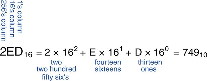
Figure 1.6 Conversion of a hexadecimal number to decimal
Example 1.4 Binary to Hexadecimal Conversion
Convert the binary number 11110102 to hexadecimal.
Solution
Again, conversion is easy. Start reading from the right. The four least significant bits are 10102 = A16. The next bits are 1112 = 716. Hence 11110102 = 7A16.
Example 1.5 Decimal to Hexadecimal and Binary Conversion
Convert the decimal number 33310 to hexadecimal and binary.
Solution
Like decimal to binary conversion, decimal to hexadecimal conversion can be done from the left or the right.
Working from the left, start with the largest power of 16 less than or equal to the number (in this case, 256). 256 goes into 333 once, so there is a 1 in the 256’s column, leaving 333 − 256 = 77. 16 goes into 77 four times, so there is a 4 in the 16’s column, leaving 77 − 16 × 4 = 13. 1310 = D16, so there is a D in the 1’s column. In summary, 33310 = 14D16. Now it is easy to convert from hexadecimal to binary, as in Example 1.3. 14D16 = 1010011012.
Working from the right, repeatedly divide the number by 16. The remainder goes in each column. 333/16 = 20 with a remainder of 1310 = D16 going in the 1’s column. 20/16 = 1 with a remainder of 4 going in the 16’s column. 1/16 = 0 with a remainder of 1 going in the 256’s column. Again, the result is 14D16.
1.4.4 Bytes, Nibbles, and All That Jazz
A group of eight bits is called a byte. It represents one of 28 = 256 possibilities. The size of objects stored in computer memories is customarily measured in bytes rather than bits.
A group of four bits, or half a byte, is called a nibble. It represents one of 24 = 16 possibilities. One hexadecimal digit stores one nibble and two hexadecimal digits store one full byte. Nibbles are no longer a commonly used unit, but the term is cute.
Microprocessors handle data in chunks called words. The size of a word depends on the architecture of the microprocessor. When this chapter was written in 2012, most computers had 64-bit processors, indicating that they operate on 64-bit words. At the time, older computers handling 32-bit words were also widely available. Simpler microprocessors, especially those used in gadgets such as toasters, use 8- or 16-bit words.
Within a group of bits, the bit in the 1’s column is called the least significant bit (lsb), and the bit at the other end is called the most significant bit (msb), as shown in Figure 1.7(a) for a 6-bit binary number. Similarly, within a word, the bytes are identified as least significant byte (LSB) through most significant byte (MSB), as shown in Figure 1.7(b) for a four-byte number written with eight hexadecimal digits.
A microprocessor is a processor built on a single chip. Until the 1970’s, processors were too complicated to fit on one chip, so mainframe processors were built from boards containing many chips. Intel introduced the first 4-bit microprocessor, called the 4004, in 1971. Now, even the most sophisticated supercomputers are built using microprocessors. We will use the terms microprocessor and processor interchangeably throughout this book.
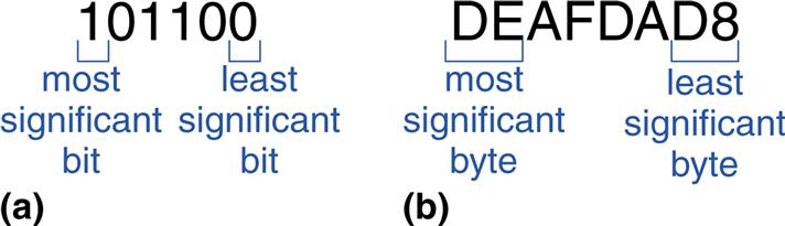
Figure 1.7 Least and most significant bits and bytes
By handy coincidence, 210 = 1024 ≈ 103. Hence, the term kilo (Greek for thousand) indicates 210. For example, 210 bytes is one kilobyte (1 KB). Similarly, mega (million) indicates 220 ≈ 106, and giga (billion) indicates 230 ≈ 109. If you know 210 ≈ 1 thousand, 220 ≈ 1 million, 230 ≈ 1 billion, and remember the powers of two up to 29, it is easy to estimate any power of two in your head.
Example 1.6 Estimating Powers of Two
Find the approximate value of 224 without using a calculator.
Solution
Split the exponent into a multiple of ten and the remainder.
224 = 220 × 24. 220 ≈ 1 million. 24 = 16. So 224 ≈ 16 million. Technically, 224 = 16,777,216, but 16 million is close enough for marketing purposes.
1024 bytes is called a kilobyte (KB). 1024 bits is called a kilobit (Kb or Kbit). Similarly, MB, Mb, GB, and Gb are used for millions and billions of bytes and bits. Memory capacity is usually measured in bytes. Communication speed is usually measured in bits/sec. For example, the maximum speed of a dial-up modem is usually 56 kbits/sec.
1.4.5 Binary Addition
Binary addition is much like decimal addition, but easier, as shown in Figure 1.8. As in decimal addition, if the sum of two numbers is greater than what fits in a single digit, we carry a 1 into the next column. Figure 1.8 compares addition of decimal and binary numbers. In the right-most column of Figure 1.8(a), 7 + 9 = 16, which cannot fit in a single digit because it is greater than 9. So we record the 1’s digit, 6, and carry the 10’s digit, 1, over to the next column. Likewise, in binary, if the sum of two numbers is greater than 1, we carry the 2’s digit over to the next column. For example, in the right-most column of Figure 1.8(b), the sum 1 + 1 = 210 = 102 cannot fit in a single binary digit. So we record the 1’s digit (0) and carry the 2’s digit (1) of the result to the next column. In the second column, the sum is 1 + 1 + 1 = 310 = 112. Again, we record the 1’s digit (1) and carry the 2’s digit (1) to the next column. For obvious reasons, the bit that is carried over to the neighboring column is called the carry bit.
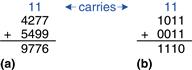
Figure 1.8 Addition examples showing carries: (a) decimal (b) binary
Example 1.7 Binary Addition
Compute 01112 + 01012.
Solution
Figure 1.9 shows that the sum is 11002. The carries are indicated in blue. We can check our work by repeating the computation in decimal. 01112 = 710. 01012 = 510. The sum is 1210 = 11002.

Figure 1.9 Binary addition example
Digital systems usually operate on a fixed number of digits. Addition is said to overflow if the result is too big to fit in the available digits. A 4-bit number, for example, has the range [0, 15]. 4-bit binary addition overflows if the result exceeds 15. The fifth bit is discarded, producing an incorrect result in the remaining four bits. Overflow can be detected by checking for a carry out of the most significant column.
Example 1.8 Addition with Overflow
Compute 11012 + 01012. Does overflow occur?
Solution
Figure 1.10 shows the sum is 100102. This result overflows the range of a 4-bit binary number. If it must be stored as four bits, the most significant bit is discarded, leaving the incorrect result of 00102. If the computation had been done using numbers with five or more bits, the result 100102 would have been correct.

Figure 1.10 Binary addition example with overflow
1.4.6 Signed Binary Numbers
So far, we have considered only unsigned binary numbers that represent positive quantities. We will often want to represent both positive and negative numbers, requiring a different binary number system. Several schemes exist to represent signed binary numbers; the two most widely employed are called sign/magnitude and two’s complement.
Sign/Magnitude Numbers
Sign/magnitude numbers are intuitively appealing because they match our custom of writing negative numbers with a minus sign followed by the magnitude. An N-bit sign/magnitude number uses the most significant bit as the sign and the remaining N−1 bits as the magnitude (absolute value). A sign bit of 0 indicates positive and a sign bit of 1 indicates negative.
The $7 billion Ariane 5 rocket, launched on June 4, 1996, veered off course 40 seconds after launch, broke up, and exploded. The failure was caused when the computer controlling the rocket overflowed its 16-bit range and crashed.
The code had been extensively tested on the Ariane 4 rocket. However, the Ariane 5 had a faster engine that produced larger values for the control computer, leading to the overflow.

Photograph courtesy of ESA/CNES/ARIANESPACE-Service Optique CS6.
Example 1.9 Sign/Magnitude Numbers
Write 5 and −5 as 4-bit sign/magnitude numbers
Solution
Both numbers have a magnitude of 510 = 1012. Thus, 510 = 01012 and −510 = 11012.
Unfortunately, ordinary binary addition does not work for sign/magnitude numbers. For example, using ordinary addition on −510 + 510 gives 11012 + 01012 = 100102, which is nonsense.
An N-bit sign/magnitude number spans the range [−2N−1 + 1, 2N−1 − 1]. Sign/magnitude numbers are slightly odd in that both +0 and −0 exist. Both indicate zero. As you may expect, it can be troublesome to have two different representations for the same number.
Two’s Complement Numbers
Two’s complement numbers are identical to unsigned binary numbers except that the most significant bit position has a weight of −2N−1 instead of 2N−1. They overcome the shortcomings of sign/magnitude numbers: zero has a single representation, and ordinary addition works.
In two’s complement representation, zero is written as all zeros: 00…0002. The most positive number has a 0 in the most significant position and 1’s elsewhere: 01…1112 = 2N−1 − 1. The most negative number has a 1 in the most significant position and 0’s elsewhere: 10…0002 = −2N−1. And −1 is written as all ones: 11…1112.
Notice that positive numbers have a 0 in the most significant position and negative numbers have a 1 in this position, so the most significant bit can be viewed as the sign bit. However, the remaining bits are interpreted differently for two’s complement numbers than for sign/magnitude numbers.
The sign of a two’s complement number is reversed in a process called taking the two’s complement. The process consists of inverting all of the bits in the number, then adding 1 to the least significant bit position. This is useful to find the representation of a negative number or to determine the magnitude of a negative number.
Example 1.10 Two’s Complement Representation of a Negative Number
Find the representation of −210 as a 4-bit two’s complement number.
Solution
Start with + 210 = 00102. To get −210, invert the bits and add 1. Inverting 00102 produces 11012. 11012 + 1 = 11102. So −210 is 11102.
Example 1.11 Value of Negative Two’s Complement Numbers
Find the decimal value of the two’s complement number 10012.
Solution
10012 has a leading 1, so it must be negative. To find its magnitude, invert the bits and add 1. Inverting 10012 = 01102. 01102 + 1 = 01112 = 710. Hence, 10012 = −710.
Two’s complement numbers have the compelling advantage that addition works properly for both positive and negative numbers. Recall that when adding N-bit numbers, the carry out of the Nth bit (i.e., the N + 1th result bit) is discarded.
Example 1.12 Adding Two’s Complement Numbers
Compute (a) −210 + 110 and (b) −710 + 710 using two’s complement numbers.
Solution
(a) −210 + 110 = 11102 + 00012 = 11112 = −110. (b) −710 + 710 = 10012 + 01112 = 100002. The fifth bit is discarded, leaving the correct 4-bit result 00002.
Subtraction is performed by taking the two’s complement of the second number, then adding.
Example 1.13 Subtracting Two’s Complement Numbers
Compute (a) 510 − 310 and (b) 310 − 510 using 4-bit two’s complement numbers.
Solution
(a) 310 = 00112. Take its two’s complement to obtain −310 = 11012. Now add 510 + (−310) = 01012 + 11012 = 00102 = 210. Note that the carry out of the most significant position is discarded because the result is stored in four bits. (b) Take the two’s complement of 510 to obtain −510 = 1011. Now add 310 + (−510) = 00112 + 10112 = 11102 = −210.
The two’s complement of 0 is found by inverting all the bits (producing 11…1112) and adding 1, which produces all 0’s, disregarding the carry out of the most significant bit position. Hence, zero is always represented with all 0’s. Unlike the sign/magnitude system, the two’s complement system has no separate −0. Zero is considered positive because its sign bit is 0.
Like unsigned numbers, N-bit two’s complement numbers represent one of 2N possible values. However the values are split between positive and negative numbers. For example, a 4-bit unsigned number represents 16 values: 0 to 15. A 4-bit two’s complement number also represents 16 values: −8 to 7. In general, the range of an N-bit two’s complement number spans [−2N−1, 2N−1 − 1]. It should make sense that there is one more negative number than positive number because there is no −0. The most negative number 10…0002 = −2N−1 is sometimes called the weird number. Its two’s complement is found by inverting the bits (producing 01…1112) and adding 1, which produces 10…0002, the weird number, again. Hence, this negative number has no positive counterpart.
Adding two N-bit positive numbers or negative numbers may cause overflow if the result is greater than 2N−1 − 1 or less than −2N−1. Adding a positive number to a negative number never causes overflow. Unlike unsigned numbers, a carry out of the most significant column does not indicate overflow. Instead, overflow occurs if the two numbers being added have the same sign bit and the result has the opposite sign bit.
Example 1.14 Adding Two’s Complement Numbers with Overflow
Compute 410 + 510 using 4-bit two’s complement numbers. Does the result overflow?
Solution
410 + 510 = 01002 + 01012 = 10012 = −710. The result overflows the range of 4-bit positive two’s complement numbers, producing an incorrect negative result. If the computation had been done using five or more bits, the result 010012 = 910 would have been correct.
When a two’s complement number is extended to more bits, the sign bit must be copied into the most significant bit positions. This process is called sign extension. For example, the numbers 3 and −3 are written as 4-bit two’s complement numbers 0011 and 1101, respectively. They are sign-extended to seven bits by copying the sign bit into the three new upper bits to form 0000011 and 1111101, respectively.
Comparison of Number Systems
The three most commonly used binary number systems are unsigned, two’s complement, and sign/magnitude. Table 1.3 compares the range of N-bit numbers in each of these three systems. Two’s complement numbers are convenient because they represent both positive and negative integers and because ordinary addition works for all numbers. Subtraction is performed by negating the second number (i.e., taking the two’s complement), and then adding. Unless stated otherwise, assume that all signed binary numbers use two’s complement representation.
Table 1.3 Range of N-bit numbers
| System | Range |
| Unsigned | [0, 2N – 1] |
| Sign/Magnitude | [–2N–1 + 1, 2N–1 – 1] |
| Two’s Complement | [–2N–1, 2N–1 – 1] |
Figure 1.11 shows a number line indicating the values of 4-bit numbers in each system. Unsigned numbers span the range [0, 15] in regular binary order. Two’s complement numbers span the range [−8, 7]. The nonnegative numbers [0, 7] share the same encodings as unsigned numbers. The negative numbers [−8, −1] are encoded such that a larger unsigned binary value represents a number closer to 0. Notice that the weird number, 1000, represents −8 and has no positive counterpart. Sign/magnitude numbers span the range [−7, 7]. The most significant bit is the sign bit. The positive numbers [1, 7] share the same encodings as unsigned numbers. The negative numbers are symmetric but have the sign bit set. 0 is represented by both 0000 and 1000. Thus, N-bit sign/magnitude numbers represent only 2N − 1 integers because of the two representations for 0.
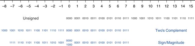
Figure 1.11 Number line and 4-bit binary encodings
1.5 Logic Gates
Now that we know how to use binary variables to represent information, we explore digital systems that perform operations on these binary variables. Logic gates are simple digital circuits that take one or more binary inputs and produce a binary output. Logic gates are drawn with a symbol showing the input (or inputs) and the output. Inputs are usually drawn on the left (or top) and outputs on the right (or bottom). Digital designers typically use letters near the beginning of the alphabet for gate inputs and the letter Y for the gate output. The relationship between the inputs and the output can be described with a truth table or a Boolean equation. A truth table lists inputs on the left and the corresponding output on the right. It has one row for each possible combination of inputs. A Boolean equation is a mathematical expression using binary variables.
1.5.1 NOT Gate
A NOT gate has one input, A, and one output, Y, as shown in Figure 1.12. The NOT gate’s output is the inverse of its input. If A is FALSE, then Y is TRUE. If A is TRUE, then Y is FALSE. This relationship is summarized by the truth table and Boolean equation in the figure. The line over A in the Boolean equation is pronounced NOT, so ![]() is read “Y equals NOT A.” The NOT gate is also called an inverter.
is read “Y equals NOT A.” The NOT gate is also called an inverter.
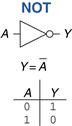
Figure 1.12 NOT gate
Other texts use a variety of notations for NOT, including Y = A′, Y = ¬A, Y = !A or Y = ~A. We will use ![]() exclusively, but don’t be puzzled if you encounter another notation elsewhere.
exclusively, but don’t be puzzled if you encounter another notation elsewhere.
1.5.2 Buffer
The other one-input logic gate is called a buffer and is shown in Figure 1.13. It simply copies the input to the output.
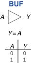
Figure 1.13 Buffer
From the logical point of view, a buffer is no different from a wire, so it might seem useless. However, from the analog point of view, the buffer might have desirable characteristics such as the ability to deliver large amounts of current to a motor or the ability to quickly send its output to many gates. This is an example of why we need to consider multiple levels of abstraction to fully understand a system; the digital abstraction hides the real purpose of a buffer.
The triangle symbol indicates a buffer. A circle on the output is called a bubble and indicates inversion, as was seen in the NOT gate symbol of Figure 1.12.
1.5.3 AND Gate
Two-input logic gates are more interesting. The AND gate shown in Figure 1.14 produces a TRUE output, Y, if and only if both A and B are TRUE. Otherwise, the output is FALSE. By convention, the inputs are listed in the order 00, 01, 10, 11, as if you were counting in binary. The Boolean equation for an AND gate can be written in several ways: Y = A • B, Y = AB, or Y = A ∩ B. The ∩ symbol is pronounced “intersection” and is preferred by logicians. We prefer Y = AB, read “Y equals A and B,” because we are lazy.
According to Larry Wall, inventor of the Perl programming language, “the three principal virtues of a programmer are Laziness, Impatience, and Hubris.”
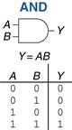
Figure 1.14 AND gate
1.5.4 OR Gate
The OR gate shown in Figure 1.15 produces a TRUE output, Y, if either A or B (or both) are TRUE. The Boolean equation for an OR gate is written as Y = A + B or Y = A ∪ B. The ∪ symbol is pronounced union and is preferred by logicians. Digital designers normally use the + notation, Y = A + B is pronounced “Y equals A or B.”
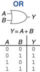
Figure 1.15 OR gate
1.5.5 Other Two-Input Gates
Figure 1.16 shows other common two-input logic gates. XOR (exclusive OR, pronounced “ex-OR”) is TRUE if A or B, but not both, are TRUE. Any gate can be followed by a bubble to invert its operation. The NAND gate performs NOT AND. Its output is TRUE unless both inputs are TRUE. The NOR gate performs NOT OR. Its output is TRUE if neither A nor B is TRUE. An N-input XOR gate is sometimes called a parity gate and produces a TRUE output if an odd number of inputs are TRUE. As with two-input gates, the input combinations in the truth table are listed in counting order.
A silly way to remember the OR symbol is that its input side is curved like Pacman’s mouth, so the gate is hungry and willing to eat any TRUE inputs it can find!

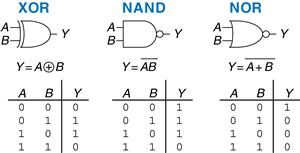
Figure 1.16 More two-input logic gates
Example 1.15 XNOR Gate
Figure 1.17 shows the symbol and Boolean equation for a two-input XNOR gate that performs the inverse of an XOR. Complete the truth table.
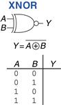
Figure 1.17 XNOR gate
Solution
Figure 1.18 shows the truth table. The XNOR output is TRUE if both inputs are FALSE or both inputs are TRUE. The two-input XNOR gate is sometimes called an equality gate because its output is TRUE when the inputs are equal.

Figure 1.18 XNOR truth table
1.5.6 Multiple-Input Gates
Many Boolean functions of three or more inputs exist. The most common are AND, OR, XOR, NAND, NOR, and XNOR. An N-input AND gate produces a TRUE output when all N inputs are TRUE. An N-input OR gate produces a TRUE output when at least one input is TRUE.
Example 1.16 Three-Input NOR Gate
Figure 1.19 shows the symbol and Boolean equation for a three-input NOR gate. Complete the truth table.
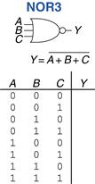
Figure 1.19 Three-input NOR gate
Solution
Figure 1.20 shows the truth table. The output is TRUE only if none of the inputs are TRUE.
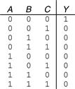
Figure 1.20 Three-input NOR truth table
Example 1.17 Four-Input AND Gate
Figure 1.21 shows the symbol and Boolean equation for a four-input AND gate. Create a truth table.

Figure 1.21 Four-input AND gate
Solution
Figure 1.22 shows the truth table. The output is TRUE only if all of the inputs are TRUE.
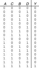
Figure 1.22 Four-input AND truth table
1.6 Beneath the Digital Abstraction
A digital system uses discrete-valued variables. However, the variables are represented by continuous physical quantities such as the voltage on a wire, the position of a gear, or the level of fluid in a cylinder. Hence, the designer must choose a way to relate the continuous value to the discrete value.
For example, consider representing a binary signal A with a voltage on a wire. Let 0 volts (V) indicate A = 0 and 5 V indicate A = 1. Any real system must tolerate some noise, so 4.97 V probably ought to be interpreted as A = 1 as well. But what about 4.3 V? Or 2.8 V? Or 2.500000 V?
1.6.1 Supply Voltage
Suppose the lowest voltage in the system is 0 V, also called ground or GND. The highest voltage in the system comes from the power supply and is usually called VDD. In 1970’s and 1980’s technology, VDD was generally 5 V. As chips have progressed to smaller transistors, VDD has dropped to 3.3 V, 2.5 V, 1.8 V, 1.5 V, 1.2 V, or even lower to save power and avoid overloading the transistors.
1.6.2 Logic Levels
The mapping of a continuous variable onto a discrete binary variable is done by defining logic levels, as shown in Figure 1.23. The first gate is called the driver and the second gate is called the receiver. The output of the driver is connected to the input of the receiver. The driver produces a LOW (0) output in the range of 0 to VOL or a HIGH (1) output in the range of VOH to VDD· If the receiver gets an input in the range of 0 to VIL, it will consider the input to be LOW. If the receiver gets an input in the range of VIH to VDD, it will consider the input to be HIGH. If, for some reason such as noise or faulty components, the receiver’s input should fall in the forbidden zone between VIL and VIH, the behavior of the gate is unpredictable. VOH,VOL,VIH, and VIL are called the output and input high and low logic levels.
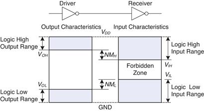
Figure 1.23 Logic levels and noise margins
1.6.3 Noise Margins
If the output of the driver is to be correctly interpreted at the input of the receiver, we must choose VOL < VIL and VOH > VIH. Thus, even if the output of the driver is contaminated by some noise, the input of the receiver will still detect the correct logic level. The noise margin is the amount of noise that could be added to a worst-case output such that the signal can still be interpreted as a valid input. As can be seen in Figure 1.23, the low and high noise margins are, respectively
![]() (1.2)
(1.2)
![]() (1.3)
(1.3)
Example 1.18 Calculating Noise Margins
Consider the inverter circuit of Figure 1.24. VO1 is the output voltage of inverter I1, and VI2 is the input voltage of inverter I2. Both inverters have the following characteristics: VDD = 5 V, VIL = 1.35 V, VIH = 3.15 V, VOL = 0.33 V, and VOH = 3.84 V. What are the inverter low and high noise margins? Can the circuit tolerate 1 V of noise between VO1 and VI2?
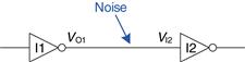
Figure 1.24 Inverter circuit
Solution
The inverter noise margins are: NML = VIL − VOL = (1.35 V − 0.33 V) = 1.02 V, NMH = VOH − VIH = (3.84 V − 3.15 V) = 0.69 V. The circuit can tolerate 1 V of noise when the output is LOW (NML = 1.02 V) but not when the output is HIGH (NMH = 0.69 V). For example, suppose the driver, I1, outputs its worst-case HIGH value, VO1 = VOH = 3.84 V. If noise causes the voltage to droop by 1 V before reaching the input of the receiver, VI2 = (3.84 V − 1 V) = 2.84 V. This is less than the acceptable input HIGH value, VIH = 3.15 V, so the receiver may not sense a proper HIGH input.
VDD stands for the voltage on the drain of a metal-oxide-semiconductor transistor, used to build most modern chips. The power supply voltage is also sometimes called VCC, standing for the voltage on the collector of a bipolar junction transistor used to build chips in an older technology. Ground is sometimes called VSS because it is the voltage on the source of a metal-oxide-semiconductor transistor. See Section 1.7 for more information on transistors.
DC indicates behavior when an input voltage is held constant or changes slowly enough for the rest of the system to keep up. The term’s historical root comes from direct current, a method of transmitting power across a line with a constant voltage. In contrast, the transient response of a circuit is the behavior when an input voltage changes rapidly. Section 2.9 explores transient response further.
1.6.4 DC Transfer Characteristics
To understand the limits of the digital abstraction, we must delve into the analog behavior of a gate. The DC transfer characteristics of a gate describe the output voltage as a function of the input voltage when the input is changed slowly enough that the output can keep up. They are called transfer characteristics because they describe the relationship between input and output voltages.
An ideal inverter would have an abrupt switching threshold at VDD/2, as shown in Figure 1.25(a). For V(A) < VDD/2, V(Y) = VDD. For V(A) > VDD/2,V(Y) = 0. In such a case, VIH = VIL = VDD/2. VOH = VDD and VOL = 0.

Figure 1.25 DC transfer characteristics and logic levels
A real inverter changes more gradually between the extremes, as shown in Figure 1.25(b). When the input voltage V(A) is 0, the output voltage V(Y) = VDD. When V(A) = VDD, V(Y) = 0. However, the transition between these endpoints is smooth and may not be centered at exactly VDD/2. This raises the question of how to define the logic levels.
A reasonable place to choose the logic levels is where the slope of the transfer characteristic dV(Y) / dV(A) is −1. These two points are called the unity gain points. Choosing logic levels at the unity gain points usually maximizes the noise margins. If VIL were reduced, VOH would only increase by a small amount. But if VIL were increased, VOH would drop precipitously.
1.6.5 The Static Discipline
To avoid inputs falling into the forbidden zone, digital logic gates are designed to conform to the static discipline. The static discipline requires that, given logically valid inputs, every circuit element will produce logically valid outputs.
By conforming to the static discipline, digital designers sacrifice the freedom of using arbitrary analog circuit elements in return for the simplicity and robustness of digital circuits. They raise the level of abstraction from analog to digital, increasing design productivity by hiding needless detail.
The choice of VDD and logic levels is arbitrary, but all gates that communicate must have compatible logic levels. Therefore, gates are grouped into logic families such that all gates in a logic family obey the static discipline when used with other gates in the family. Logic gates in the same logic family snap together like Legos in that they use consistent power supply voltages and logic levels.
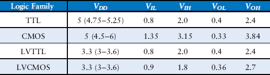
Four major logic families that predominated from the 1970’s through the 1990’s are Transistor-Transistor Logic (TTL), Complementary Metal-Oxide-Semiconductor Logic (CMOS, pronounced sea-moss), Low Voltage TTL Logic (LVTTL), and Low Voltage CMOS Logic (LVCMOS). Their logic levels are compared in Table 1.4. Since then, logic families have balkanized with a proliferation of even lower power supply voltages. Appendix A.6 revisits popular logic families in more detail.
Table 1.4 Logic levels of 5 V and 3.3 V logic families
Example 1.19 Logic Family Compatibility
Which of the logic families in Table 1.4 can communicate with each other reliably?
Solution
Table 1.5 lists which logic families have compatible logic levels. Note that a 5 V logic family such as TTL or CMOS may produce an output voltage as HIGH as 5 V. If this 5 V signal drives the input of a 3.3 V logic family such as LVTTL or LVCMOS, it can damage the receiver, unless the receiver is specially designed to be “5-volt compatible.”
Table 1.5 Compatibility of logic families
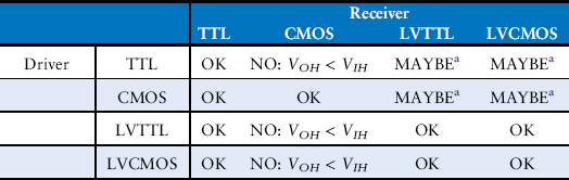
a As long as a 5 V HIGH level does not damage the receiver input
Robert Noyce, 1927–1990
Born in Burlington, Iowa. Received a B.A. in physics from Grinnell College and a Ph.D. in physics from MIT. Nicknamed “Mayor of Silicon Valley” for his profound influence on the industry.
Cofounded Fairchild Semiconductor in 1957 and Intel in 1968. Coinvented the integrated circuit. Many engineers from his teams went on to found other seminal semiconductor companies (© 2006, Intel Corporation. Reproduced by permission).
1.7 CMOS Transistors*
This section and other sections marked with a * are optional and are not necessary to understand the main flow of the book.
Babbage’s Analytical Engine was built from gears, and early electrical computers used relays or vacuum tubes. Modern computers use transistors because they are cheap, small, and reliable. Transistors are electrically controlled switches that turn ON or OFF when a voltage or current is applied to a control terminal. The two main types of transistors are bipolar junction transistors and metal-oxide-semiconductor field effect transistors (MOSFETs or MOS transistors, pronounced “moss-fets” or “M-O-S”, respectively).
In 1958, Jack Kilby at Texas Instruments built the first integrated circuit containing two transistors. In 1959, Robert Noyce at Fairchild Semiconductor patented a method of interconnecting multiple transistors on a single silicon chip. At the time, transistors cost about $10 each.
Thanks to more than three decades of unprecedented manufacturing advances, engineers can now pack roughly one billion MOSFETs onto a 1 cm2 chip of silicon, and these transistors cost less than 10 microcents apiece. The capacity and cost continue to improve by an order of magnitude every 8 years or so. MOSFETs are now the building blocks of almost all digital systems. In this section, we will peer beneath the digital abstraction to see how logic gates are built from MOSFETs.
1.7.1 Semiconductors
MOS transistors are built from silicon, the predominant atom in rock and sand. Silicon (Si) is a group IV atom, so it has four electrons in its valence shell and forms bonds with four adjacent atoms, resulting in a crystalline lattice. Figure 1.26(a) shows the lattice in two dimensions for ease of drawing, but remember that the lattice actually forms a cubic crystal. In the figure, a line represents a covalent bond. By itself, silicon is a poor conductor because all the electrons are tied up in covalent bonds. However, it becomes a better conductor when small amounts of impurities, called dopant atoms, are carefully added. If a group V dopant such as arsenic (As) is added, the dopant atoms have an extra electron that is not involved in the bonds. The electron can easily move about the lattice, leaving an ionized dopant atom (As+) behind, as shown in Figure 1.26(b). The electron carries a negative charge, so we call arsenic an n-type dopant. On the other hand, if a group III dopant such as boron (B) is added, the dopant atoms are missing an electron, as shown in Figure 1.26(c). This missing electron is called a hole. An electron from a neighboring silicon atom may move over to fill the missing bond, forming an ionized dopant atom (B−) and leaving a hole at the neighboring silicon atom. In a similar fashion, the hole can migrate around the lattice. The hole is a lack of negative charge, so it acts like a positively charged particle. Hence, we call boron a p-type dopant. Because the conductivity of silicon changes over many orders of magnitude depending on the concentration of dopants, silicon is called a semiconductor.
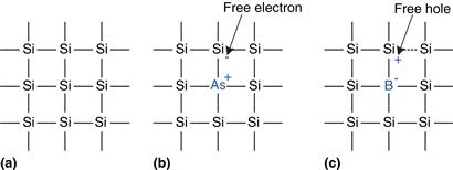
Figure 1.26 Silicon lattice and dopant atoms
1.7.2 Diodes
The junction between p-type and n-type silicon is called a diode. The p-type region is called the anode and the n-type region is called the cathode, as illustrated in Figure 1.27. When the voltage on the anode rises above the voltage on the cathode, the diode is forward biased, and current flows through the diode from the anode to the cathode. But when the anode voltage is lower than the voltage on the cathode, the diode is reverse biased, and no current flows. The diode symbol intuitively shows that current only flows in one direction.
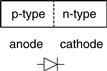
Figure 1.27 The p-n junction diode structure and symbol
1.7.3 Capacitors
A capacitor consists of two conductors separated by an insulator. When a voltage V is applied to one of the conductors, the conductor accumulates electric charge Q and the other conductor accumulates the opposite charge −Q. The capacitance C of the capacitor is the ratio of charge to voltage: C = Q/V. The capacitance is proportional to the size of the conductors and inversely proportional to the distance between them. The symbol for a capacitor is shown in Figure 1.28.
![]()
Figure 1.28 Capacitor symbol
Capacitance is important because charging or discharging a conductor takes time and energy. More capacitance means that a circuit will be slower and require more energy to operate. Speed and energy will be discussed throughout this book.

Technicians in an Intel clean room wear Gore-Tex bunny suits to prevent particulates from their hair, skin, and clothing from contaminating the microscopic transistors on silicon wafers (© 2006, Intel Corporation. Reproduced by permission).
1.7.4 nMOS and pMOS Transistors
A MOSFET is a sandwich of several layers of conducting and insulating materials. MOSFETs are built on thin flat wafers of silicon of about 15 to 30 cm in diameter. The manufacturing process begins with a bare wafer. The process involves a sequence of steps in which dopants are implanted into the silicon, thin films of silicon dioxide and silicon are grown, and metal is deposited. Between each step, the wafer is patterned so that the materials appear only where they are desired. Because transistors are a fraction of a micron2 in length and the entire wafer is processed at once, it is inexpensive to manufacture billions of transistors at a time. Once processing is complete, the wafer is cut into rectangles called chips or dice that contain thousands, millions, or even billions of transistors. The chip is tested, then placed in a plastic or ceramic package with metal pins to connect it to a circuit board.
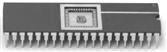
A 40-pin dual-inline package (DIP) contains a small chip (scarcely visible) in the center that is connected to 40 metal pins, 20 on a side, by gold wires thinner than a strand of hair (photograph by Kevin Mapp. © Harvey Mudd College).
The MOSFET sandwich consists of a conducting layer called the gate on top of an insulating layer of silicon dioxide (SiO2) on top of the silicon wafer, called the substrate. Historically, the gate was constructed from metal, hence the name metal-oxide-semiconductor. Modern manufacturing processes use polycrystalline silicon for the gate because it does not melt during subsequent high-temperature processing steps. Silicon dioxide is better known as glass and is often simply called oxide in the semiconductor industry. The metal-oxide-semiconductor sandwich forms a capacitor, in which a thin layer of insulating oxide called a dielectric separates the metal and semiconductor plates.
The source and drain terminals are physically symmetric. However, we say that charge flows from the source to the drain. In an nMOS transistor, the charge is carried by electrons, which flow from negative voltage to positive voltage. In a pMOS transistor, the charge is carried by holes, which flow from positive voltage to negative voltage. If we draw schematics with the most positive voltage at the top and the most negative at the bottom, the source of (negative) charges in an nMOS transistor is the bottom terminal and the source of (positive) charges in a pMOS transistor is the top terminal.
There are two flavors of MOSFETs: nMOS and pMOS (pronounced “n-moss” and “p-moss”). Figure 1.29 shows cross-sections of each type, made by sawing through a wafer and looking at it from the side. The n-type transistors, called nMOS, have regions of n-type dopants adjacent to the gate called the source and the drain and are built on a p-type semiconductor substrate. The pMOS transistors are just the opposite, consisting of p-type source and drain regions in an n-type substrate.
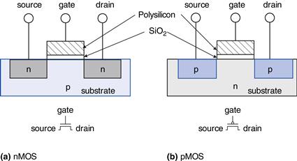
Figure 1.29 nMOS and pMOS transistors
A MOSFET behaves as a voltage-controlled switch in which the gate voltage creates an electric field that turns ON or OFF a connection between the source and drain. The term field effect transistor comes from this principle of operation. Let us start by exploring the operation of an nMOS transistor.
The substrate of an nMOS transistor is normally tied to GND, the lowest voltage in the system. First, consider the situation when the gate is also at 0 V, as shown in Figure 1.30(a). The diodes between the source or drain and the substrate are reverse biased because the source or drain voltage is nonnegative. Hence, there is no path for current to flow between the source and drain, so the transistor is OFF. Now, consider when the gate is raised to VDD, as shown in Figure 1.30(b). When a positive voltage is applied to the top plate of a capacitor, it establishes an electric field that attracts positive charge on the top plate and negative charge to the bottom plate. If the voltage is sufficiently large, so much negative charge is attracted to the underside of the gate that the region inverts from p-type to effectively become n-type. This inverted region is called the channel. Now the transistor has a continuous path from the n-type source through the n-type channel to the n-type drain, so electrons can flow from source to drain. The transistor is ON. The gate voltage required to turn on a transistor is called the threshold voltage,Vt, and is typically 0.3 to 0.7 V.

A technician holds a 12-inch wafer containing hundreds of microprocessor chips (© 2006, Intel Corporation. Reproduced by permission).
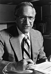
Gordon Moore, 1929–
Born in San Francisco. Received a B.S. in chemistry from UC Berkeley and a Ph.D. in chemistry and physics from Caltech. Cofounded Intel in 1968 with Robert Noyce. Observed in 1965 that the number of transistors on a computer chip doubles every year. This trend has become known as Moore’s Law. Since 1975, transistor counts have doubled every two years.
A corollary of Moore’s Law is that microprocessor performance doubles every 18 to 24 months. Semiconductor sales have also increased exponentially. Unfortunately, power consumption has increased exponentially as well (© 2006, Intel Corporation. Reproduced by permission).
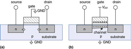
Figure 1.30 nMOS transistor operation
pMOS transistors work in just the opposite fashion, as might be guessed from the bubble on their symbol shown in Figure 1.31. The substrate is tied to VDD. When the gate is also at VDD, the pMOS transistor is OFF. When the gate is at GND, the channel inverts to p-type and the pMOS transistor is ON.
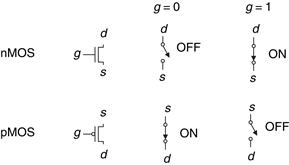
Figure 1.31 Switch models of MOSFETs
Unfortunately, MOSFETs are not perfect switches. In particular, nMOS transistors pass 0’s well but pass 1’s poorly. Specifically, when the gate of an nMOS transistor is at VDD, the drain will only swing between 0 and VDD − Vt. Similarly, pMOS transistors pass 1’s well but 0’s poorly. However, we will see that it is possible to build logic gates that use transistors only in their good mode.
nMOS transistors need a p-type substrate, and pMOS transistors need an n-type substrate. To build both flavors of transistors on the same chip, manufacturing processes typically start with a p-type wafer, then implant n-type regions called wells where the pMOS transistors should go. These processes that provide both flavors of transistors are called Complementary MOS or CMOS. CMOS processes are used to build the vast majority of all transistors fabricated today.
In summary, CMOS processes give us two types of electrically controlled switches, as shown in Figure 1.31. The voltage at the gate (g) regulates the flow of current between the source (s) and drain (d). nMOS transistors are OFF when the gate is 0 and ON when the gate is 1. pMOS transistors are just the opposite: ON when the gate is 0 and OFF when the gate is 1.
1.7.5 CMOS NOT Gate
Figure 1.32 shows a schematic of a NOT gate built with CMOS transistors. The triangle indicates GND, and the flat bar indicates VDD; these labels will be omitted from future schematics. The nMOS transistor, N1, is connected between GND and the Y output. The pMOS transistor, P1, is connected between VDD and the Y output. Both transistor gates are controlled by the input, A.
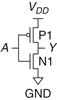
Figure 1.32 NOT gate schematic
If A = 0, N1 is OFF and P1 is ON. Hence, Y is connected to VDD but not to GND, and is pulled up to a logic 1. P1 passes a good 1. If A = 1, N1 is ON and P1 is OFF, and Y is pulled down to a logic 0. N1 passes a good 0. Checking against the truth table in Figure 1.12, we see that the circuit is indeed a NOT gate.
1.7.6 Other CMOS Logic Gates
Figure 1.33 shows a schematic of a two-input NAND gate. In schematic diagrams, wires are always joined at three-way junctions. They are joined at four-way junctions only if a dot is shown. The nMOS transistors N1 and N2 are connected in series; both nMOS transistors must be ON to pull the output down to GND. The pMOS transistors P1 and P2 are in parallel; only one pMOS transistor must be ON to pull the output up to VDD. Table 1.6 lists the operation of the pull-down and pull-up networks and the state of the output, demonstrating that the gate does function as a NAND. For example, when A = 1 and B = 0, N1 is ON, but N2 is OFF, blocking the path from Y to GND. P1 is OFF, but P2 is ON, creating a path from VDD to Y. Therefore, Y is pulled up to 1.

Figure 1.33 Two-input NAND gate schematic
Table 1.6 NAND gate operation
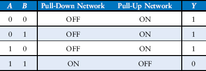
Figure 1.34 shows the general form used to construct any inverting logic gate, such as NOT, NAND, or NOR. nMOS transistors are good at passing 0’s, so a pull-down network of nMOS transistors is placed between the output and GND to pull the output down to 0. pMOS transistors are good at passing 1’s, so a pull-up network of pMOS transistors is placed between the output and VDD to pull the output up to 1. The networks may consist of transistors in series or in parallel. When transistors are in parallel, the network is ON if either transistor is ON. When transistors are in series, the network is ON only if both transistors are ON. The slash across the input wire indicates that the gate may receive multiple inputs.
Experienced designers claim that electronic devices operate because they contain magic smoke. They confirm this theory with the observation that if the magic smoke is ever let out of the device, it ceases to work.
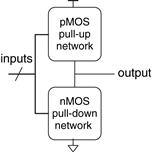
Figure 1.34 General form of an inverting logic gate
If both the pull-up and pull-down networks were ON simultaneously, a short circuit would exist between VDD and GND. The output of the gate might be in the forbidden zone and the transistors would consume large amounts of power, possibly enough to burn out. On the other hand, if both the pull-up and pull-down networks were OFF simultaneously, the output would be connected to neither VDD nor GND. We say that the output floats. Its value is again undefined. Floating outputs are usually undesirable, but in Section 2.6 we will see how they can occasionally be used to the designer’s advantage.
In a properly functioning logic gate, one of the networks should be ON and the other OFF at any given time, so that the output is pulled HIGH or LOW but not shorted or floating. We can guarantee this by using the rule of conduction complements. When nMOS transistors are in series, the pMOS transistors must be in parallel. When nMOS transistors are in parallel, the pMOS transistors must be in series.
Example 1.20 Three-Input NAND Schematic
Draw a schematic for a three-input NAND gate using CMOS transistors.
Solution
The NAND gate should produce a 0 output only when all three inputs are 1. Hence, the pull-down network should have three nMOS transistors in series. By the conduction complements rule, the pMOS transistors must be in parallel. Such a gate is shown in Figure 1.35; you can verify the function by checking that it has the correct truth table.
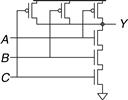
Figure 1.35 Three-input NAND gate schematic
Example 1.21 Two-Input NOR Schematic
Draw a schematic for a two-input NOR gate using CMOS transistors.
Solution
The NOR gate should produce a 0 output if either input is 1. Hence, the pull-down network should have two nMOS transistors in parallel. By the conduction complements rule, the pMOS transistors must be in series. Such a gate is shown in Figure 1.36.

Figure 1.36 Two-input NOR gate schematic
Example 1.22 Two-Input AND Schematic
Draw a schematic for a two-input AND gate.
Solution
It is impossible to build an AND gate with a single CMOS gate. However, building NAND and NOT gates is easy. Thus, the best way to build an AND gate using CMOS transistors is to use a NAND followed by a NOT, as shown in Figure 1.37.
![]()
Figure 1.37 Two-input AND gate schematic
1.7.7 Transmission Gates
At times, designers find it convenient to use an ideal switch that can pass both 0 and 1 well. Recall that nMOS transistors are good at passing 0 and pMOS transistors are good at passing 1, so the parallel combination of the two passes both values well. Figure 1.38 shows such a circuit, called a transmission gate or pass gate. The two sides of the switch are called A and B because a switch is bidirectional and has no preferred input or output side. The control signals are called enables, EN and ![]() . When EN = 0 and
. When EN = 0 and ![]() = 1, both transistors are OFF. Hence, the transmission gate is OFF or disabled, so A and B are not connected. When EN = 1 and
= 1, both transistors are OFF. Hence, the transmission gate is OFF or disabled, so A and B are not connected. When EN = 1 and ![]() = 0, the transmission gate is ON or enabled, and any logic value can flow between A and B.
= 0, the transmission gate is ON or enabled, and any logic value can flow between A and B.
![]()
Figure 1.38 Transmission gate
1.7.8 Pseudo-nMOS Logic
An N-input CMOS NOR gate uses N nMOS transistors in parallel and N pMOS transistors in series. Transistors in series are slower than transistors in parallel, just as resistors in series have more resistance than resistors in parallel. Moreover, pMOS transistors are slower than nMOS transistors because holes cannot move around the silicon lattice as fast as electrons. Therefore the parallel nMOS transistors are fast and the series pMOS transistors are slow, especially when many are in series.
Pseudo-nMOS logic replaces the slow stack of pMOS transistors with a single weak pMOS transistor that is always ON, as shown in Figure 1.39. This pMOS transistor is often called a weak pull-up. The physical dimensions of the pMOS transistor are selected so that the pMOS transistor will pull the output Y HIGH weakly—that is, only if none of the nMOS transistors are ON. But if any nMOS transistor is ON, it overpowers the weak pull-up and pulls Y down close enough to GND to produce a logic 0.
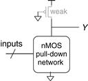
Figure 1.39 Generic pseudo-nMOS gate
The advantage of pseudo-nMOS logic is that it can be used to build fast NOR gates with many inputs. For example, Figure 1.40 shows a pseudo-nMOS four-input NOR. Pseudo-nMOS gates are useful for certain memory and logic arrays discussed in Chapter 5. The disadvantage is that a short circuit exists between VDD and GND when the output is LOW; the weak pMOS and nMOS transistors are both ON. The short circuit draws continuous power, so pseudo-nMOS logic must be used sparingly.
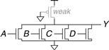
Figure 1.40 Pseudo-nMOS four-input NOR gate
Pseudo-nMOS gates got their name from the 1970’s, when manufacturing processes only had nMOS transistors. A weak nMOS transistor was used to pull the output HIGH because pMOS transistors were not available.
1.8 Power Consumption*
Power consumption is the amount of energy used per unit time. Power consumption is of great importance in digital systems. The battery life of portable systems such as cell phones and laptop computers is limited by power consumption. Power is also significant for systems that are plugged in, because electricity costs money and because the system will overheat if it draws too much power.
Digital systems draw both dynamic and static power. Dynamic power is the power used to charge capacitance as signals change between 0 and 1. Static power is the power used even when signals do not change and the system is idle.
Logic gates and the wires that connect them have capacitance. The energy drawn from the power supply to charge a capacitance C to voltage VDD is CVDD2. If the voltage on the capacitor switches at frequency f (i.e., f times per second), it charges the capacitor f/2 times and discharges it f/2 times per second. Discharging does not draw energy from the power supply, so the dynamic power consumption is
![]() (1.4)
(1.4)
Electrical systems draw some current even when they are idle. When transistors are OFF, they leak a small amount of current. Some circuits, such as the pseudo-nMOS gate discussed in Section 1.7.8, have a path from VDD to GND through which current flows continuously. The total static current, IDD, is also called the leakage current or the quiescent supply current flowing between VDD and GND. The static power consumption is proportional to this static current:
![]() (1.5)
(1.5)
Example 1.23 Power Consumption
A particular cell phone has a 6 watt-hour (W-hr) battery and operates at 1.2 V. Suppose that, when it is in use, the cell phone operates at 300 MHz and the average amount of capacitance in the chip switching at any given time is 10 nF (10−8 Farads). When in use, it also broadcasts 3 W of power out of its antenna. When the phone is not in use, the dynamic power drops to almost zero because the signal processing is turned off. But the phone also draws 40 mA of quiescent current whether it is in use or not. Determine the battery life of the phone (a) if it is not being used, and (b) if it is being used continuously.
Solution
The static power is Pstatic = (0.040 A)(1.2 V) = 48 mW. (a) If the phone is not being used, this is the only power consumption, so the battery life is (6 Whr)/(0.048 W) = 125 hours (about 5 days). (b) If the phone is being used, the dynamic power is Pdynamic = (0.5)(10−8 F)(1.2 V)2(3 × 10⁸ Hz) = 2.16 W. Together with the static and broadcast power, the total active power is 2.16 W + 0.048 W + 3 W = 5.2 W, so the battery life is 6 W-hr/5.2 W = 1.15 hours. This example somewhat oversimplifies the actual operation of a cell phone, but it illustrates the key ideas of power consumption.
1.9 Summary and a Look Ahead
There are 10 kinds of people in this world: those who can count in binary and those who can’t.
This chapter has introduced principles for understanding and designing complex systems. Although the real world is analog, digital designers discipline themselves to use a discrete subset of possible signals. In particular, binary variables have just two states: 0 and 1, also called FALSE and TRUE or LOW and HIGH. Logic gates compute a binary output from one or more binary inputs. Some of the common logic gates are:
Logic gates are commonly built from CMOS transistors, which behave as electrically controlled switches. nMOS transistors turn ON when the gate is 1. pMOS transistors turn ON when the gate is 0.
In Chapters 2 through 5, we continue the study of digital logic. Chapter 2 addresses combinational logic, in which the outputs depend only on the current inputs. The logic gates introduced already are examples of combinational logic. You will learn to design circuits involving multiple gates to implement a relationship between inputs and outputs specified by a truth table or Boolean equation. Chapter 3 addresses sequential logic, in which the outputs depend on both current and past inputs. Registers are common sequential elements that remember their previous input. Finite state machines, built from registers and combinational logic, are a powerful way to build complicated systems in a systematic fashion. We also study timing of digital systems to analyze how fast a system can operate. Chapter 4 describes hardware description languages (HDLs). HDLs are related to conventional programming languages but are used to simulate and build hardware rather than software. Most digital systems today are designed with HDLs. SystemVerilog and VHDL are the two prevalent languages, and they are covered side-by-side in this book. Chapter 5 studies other combinational and sequential building blocks such as adders, multipliers, and memories.
Chapter 6 shifts to computer architecture. It describes the MIPS processor, an industry-standard microprocessor used in consumer electronics, some Silicon Graphics workstations, and many communications systems such as televisions, networking hardware, and wireless links. The MIPS architecture is defined by its registers and assembly language instruction set. You will learn to write programs in assembly language for the MIPS processor so that you can communicate with the processor in its native language.
Chapters 7 and 8 bridge the gap between digital logic and computer architecture. Chapter 7 investigates microarchitecture, the arrangement of digital building blocks, such as adders and registers, needed to construct a processor. In that chapter, you learn to build your own MIPS processor. Indeed, you learn three microarchitectures illustrating different trade-offs of performance and cost. Processor performance has increased exponentially, requiring ever more sophisticated memory systems to feed the insatiable demand for data. Chapter 8 delves into memory system architecture and also describes how computers communicate with peripheral devices such as keyboards and printers.
Exercises
Exercise 1.1 Explain in one paragraph at least three levels of abstraction that are used by
Exercise 1.2 Explain in one paragraph how the techniques of hierarchy, modularity, and regularity may be used by
Exercise 1.3 Ben Bitdiddle is building a house. Explain how he can use the principles of hierarchy, modularity, and regularity to save time and money during construction.
Exercise 1.4 An analog voltage is in the range of 0–5 V. If it can be measured with an accuracy of ±50 mV, at most how many bits of information does it convey?
Exercise 1.5 A classroom has an old clock on the wall whose minute hand broke off.
(a) If you can read the hour hand to the nearest 15 minutes, how many bits of information does the clock convey about the time?
(b) If you know whether it is before or after noon, how many additional bits of information do you know about the time?
Exercise 1.6 The Babylonians developed the sexagesimal (base 60) number system about 4000 years ago. How many bits of information is conveyed with one sexagesimal digit? How do you write the number 400010 in sexagesimal?
Exercise 1.7 How many different numbers can be represented with 16 bits?
Exercise 1.8 What is the largest unsigned 32-bit binary number?
Exercise 1.9 What is the largest 16-bit binary number that can be represented with
Exercise 1.10 What is the largest 32-bit binary number that can be represented with
Exercise 1.11 What is the smallest (most negative) 16-bit binary number that can be represented with
Exercise 1.12 What is the smallest (most negative) 32-bit binary number that can be represented with
Exercise 1.13 Convert the following unsigned binary numbers to decimal. Show your work.
Exercise 1.14 Convert the following unsigned binary numbers to decimal. Show your work.
Exercise 1.15 Repeat Exercise 1.13, but convert to hexadecimal.
Exercise 1.16 Repeat Exercise 1.14, but convert to hexadecimal.
Exercise 1.17 Convert the following hexadecimal numbers to decimal. Show your work.
Exercise 1.18 Convert the following hexadecimal numbers to decimal. Show your work.
Exercise 1.19 Repeat Exercise 1.17, but convert to unsigned binary.
Exercise 1.20 Repeat Exercise 1.18, but convert to unsigned binary.
Exercise 1.21 Convert the following two’s complement binary numbers to decimal.
Exercise 1.22 Convert the following two’s complement binary numbers to decimal.
Exercise 1.23 Repeat Exercise 1.21, assuming the binary numbers are in sign/magnitude form rather than two’s complement representation.
Exercise 1.24 Repeat Exercise 1.22, assuming the binary numbers are in sign/magnitude form rather than two’s complement representation.
Exercise 1.25 Convert the following decimal numbers to unsigned binary numbers.
Exercise 1.26 Convert the following decimal numbers to unsigned binary numbers.
Exercise 1.27 Repeat Exercise 1.25, but convert to hexadecimal.
Exercise 1.28 Repeat Exercise 1.26, but convert to hexadecimal.
Exercise 1.29 Convert the following decimal numbers to 8-bit two’s complement numbers or indicate that the decimal number would overflow the range.
Exercise 1.30 Convert the following decimal numbers to 8-bit two’s complement numbers or indicate that the decimal number would overflow the range.
Exercise 1.31 Repeat Exercise 1.29, but convert to 8-bit sign/magnitude numbers.
Exercise 1.32 Repeat Exercise 1.30, but convert to 8-bit sign/magnitude numbers.
Exercise 1.33 Convert the following 4-bit two’s complement numbers to 8-bit two’s complement numbers.
Exercise 1.34 Convert the following 4-bit two’s complement numbers to 8-bit two’s complement numbers.
Exercise 1.35 Repeat Exercise 1.33 if the numbers are unsigned rather than two’s complement.
Exercise 1.36 Repeat Exercise 1.34 if the numbers are unsigned rather than two’s complement.
Exercise 1.37 Base 8 is referred to as octal. Convert each of the numbers from Exercise 1.25 to octal.
Exercise 1.38 Base 8 is referred to as octal. Convert each of the numbers from Exercise 1.26 to octal.
Exercise 1.39 Convert each of the following octal numbers to binary, hexadecimal, and decimal.
Exercise 1.40 Convert each of the following octal numbers to binary, hexadecimal, and decimal.
Exercise 1.41 How many 5-bit two’s complement numbers are greater than 0? How many are less than 0? How would your answers differ for sign/magnitude numbers?
Exercise 1.42 How many 7-bit two’s complement numbers are greater than 0? How many are less than 0? How would your answers differ for sign/magnitude numbers?
Exercise 1.43 How many bytes are in a 32-bit word? How many nibbles are in the word?
Exercise 1.44 How many bytes are in a 64-bit word?
Exercise 1.45 A particular DSL modem operates at 768 kbits/sec. How many bytes can it receive in 1 minute?
Exercise 1.46 USB 3.0 can send data at 5 Gbits/sec. How many bytes can it send in 1 minute?
Exercise 1.47 Hard disk manufacturers use the term “megabyte” to mean 106 bytes and “gigabyte” to mean 109 bytes. How many real GBs of music can you store on a 50 GB hard disk?
Exercise 1.48 Estimate the value of 231 without using a calculator.
Exercise 1.49 A memory on the Pentium II microprocessor is organized as a rectangular array of bits with 28 rows and 29 columns. Estimate how many bits it has without using a calculator.
Exercise 1.50 Draw a number line analogous to Figure 1.11 for 3-bit unsigned, two’s complement, and sign/magnitude numbers.
Exercise 1.51 Draw a number line analogous to Figure 1.11 for 2-bit unsigned, two’s complement, and sign/magnitude numbers.
Exercise 1.52 Perform the following additions of unsigned binary numbers. Indicate whether or not the sum overflows a 4-bit result.
Exercise 1.53 Perform the following additions of unsigned binary numbers. Indicate whether or not the sum overflows an 8-bit result.
Exercise 1.54 Repeat Exercise 1.52, assuming that the binary numbers are in two’s complement form.
Exercise 1.55 Repeat Exercise 1.53, assuming that the binary numbers are in two’s complement form.
Exercise 1.56 Convert the following decimal numbers to 6-bit two’s complement binary numbers and add them. Indicate whether or not the sum overflows a 6-bit result.
Exercise 1.57 Repeat Exercise 1.56 for the following numbers.
Exercise 1.58 Perform the following additions of unsigned hexadecimal numbers. Indicate whether or not the sum overflows an 8-bit (two hex digit) result.
Exercise 1.59 Perform the following additions of unsigned hexadecimal numbers. Indicate whether or not the sum overflows an 8-bit (two hex digit) result.
Exercise 1.60 Convert the following decimal numbers to 5-bit two’s complement binary numbers and subtract them. Indicate whether or not the difference overflows a 5-bit result.
Exercise 1.61 Convert the following decimal numbers to 6-bit two’s complement binary numbers and subtract them. Indicate whether or not the difference overflows a 6-bit result.
Exercise 1.62 In a biased N-bit binary number system with bias B, positive and negative numbers are represented as their value plus the bias B. For example, for 5-bit numbers with a bias of 15, the number 0 is represented as 01111, 1 as 10000, and so forth. Biased number systems are sometimes used in floating point mathematics, which will be discussed in Chapter 5. Consider a biased 8-bit binary number system with a bias of 12710·
(a) What decimal value does the binary number 100000102 represent?
(b) What binary number represents the value 0?
(c) What is the representation and value of the most negative number?
(d) What is the representation and value of the most positive number?
Exercise 1.63 Draw a number line analogous to Figure 1.11 for 3-bit biased numbers with a bias of 3 (see Exercise 1.62 for a definition of biased numbers).
Exercise 1.64 In a binary coded decimal (BCD) system, 4 bits are used to represent a decimal digit from 0 to 9. For example, 3710 is written as 00110111BCD.
(b) Convert 100101010001BCD to decimal
(c) Convert 01101001BCD to binary
(d) Explain why BCD might be a useful way to represent numbers
Exercise 1.65 Answer the following questions related to BCD systems (see Exercise 1.64 for the definition of BCD).
(b) Convert 000110000111BCD to decimal
(c) Convert 10010101BCD to binary
(d) Explain the disadvantages of BCD when compared to binary representations of numbers
Exercise 1.66 A flying saucer crashes in a Nebraska cornfield. The FBI investigates the wreckage and finds an engineering manual containing an equation in the Martian number system: 325 + 42 = 411. If this equation is correct, how many fingers would you expect Martians to have?
Exercise 1.67 Ben Bitdiddle and Alyssa P. Hacker are having an argument. Ben says, “All integers greater than zero and exactly divisible by six have exactly two 1’s in their binary representation.” Alyssa disagrees. She says, “No, but all such numbers have an even number of 1’s in their representation.” Do you agree with Ben or Alyssa or both or neither? Explain.
Exercise 1.68 Ben Bitdiddle and Alyssa P. Hacker are having another argument. Ben says, “I can get the two’s complement of a number by subtracting 1, then inverting all the bits of the result.” Alyssa says, “No, I can do it by examining each bit of the number, starting with the least significant bit. When the first 1 is found, invert each subsequent bit.” Do you agree with Ben or Alyssa or both or neither? Explain.
Exercise 1.69 Write a program in your favorite language (e.g., C, Java, Perl) to convert numbers from binary to decimal. The user should type in an unsigned binary number. The program should print the decimal equivalent.
Exercise 1.70 Repeat Exercise 1.69 but convert from an arbitrary base b1 to another base b2, as specified by the user. Support bases up to 16, using the letters of the alphabet for digits greater than 9. The user should enter b1, b2, and then the number to convert in base b1. The program should print the equivalent number in base b2.
Exercise 1.71 Draw the symbol, Boolean equation, and truth table for
Exercise 1.72 Draw the symbol, Boolean equation, and truth table for
Exercise 1.73 A majority gate produces a TRUE output if and only if more than half of its inputs are TRUE. Complete a truth table for the three-input majority gate shown in Figure 1.41.
![]()
Figure 1.41 Three-input majority gate
Exercise 1.74 A three-input AND-OR (AO) gate shown in Figure 1.42 produces a TRUE output if both A and B are TRUE, or if C is TRUE. Complete a truth table for the gate.
![]()
Figure 1.42 Three-input AND-OR gate
Exercise 1.75 A three-input OR-AND-INVERT (OAI) gate shown in Figure 1.43 produces a FALSE output if C is TRUE and A or B is TRUE. Otherwise it produces a TRUE output. Complete a truth table for the gate.
![]()
Figure 1.43 Three-input OR-AND-INVERT gate
Exercise 1.76 There are 16 different truth tables for Boolean functions of two variables. List each truth table. Give each one a short descriptive name (such as OR, NAND, and so on).
Exercise 1.77 How many different truth tables exist for Boolean functions of N variables?
Exercise 1.78 Is it possible to assign logic levels so that a device with the transfer characteristics shown in Figure 1.44 would serve as an inverter? If so, what are the input and output low and high levels (VIL, VOL, VIH, and VOH) and noise margins (NML and NMH)? If not, explain why not.
Figure 1.44 DC transfer characteristics
Exercise 1.79 Repeat Exercise 1.78 for the transfer characteristics shown in Figure 1.45.
Figure 1.45 DC transfer characteristics
Exercise 1.80 Is it possible to assign logic levels so that a device with the transfer characteristics shown in Figure 1.46 would serve as a buffer? If so, what are the input and output low and high levels (VIL,VOL,VIH, and VOH) and noise margins (NML and NMH)? If not, explain why not.
Figure 1.46 DC transfer characteristics
Exercise 1.81 Ben Bitdiddle has invented a circuit with the transfer characteristics shown in Figure 1.47 that he would like to use as a buffer. Will it work? Why or why not? He would like to advertise that it is compatible with LVCMOS and LVTTL logic. Can Ben’s buffer correctly receive inputs from those logic families? Can its output properly drive those logic families? Explain.

Figure 1.47 Ben’s buffer DC transfer characteristics
Exercise 1.82 While walking down a dark alley, Ben Bitdiddle encounters a two-input gate with the transfer function shown in Figure 1.48. The inputs are A and B and the output is Y.

Figure 1.48 Two-input DC transfer characteristics
Exercise 1.83 Repeat Exercise 1.82 for Figure 1.49.

Figure 1.49 Two-input DC transfer characteristics
Exercise 1.84 Sketch a transistor-level circuit for the following CMOS gates. Use a minimum number of transistors.
(b) three-input OR-AND-INVERT gate (see Exercise 1.75)
(c) three-input AND-OR gate (see Exercise 1.74)
Exercise 1.85 Sketch a transistor-level circuit for the following CMOS gates. Use a minimum number of transistors.
Exercise 1.86 A minority gate produces a TRUE output if and only if fewer than half of its inputs are TRUE. Otherwise it produces a FALSE output. Sketch a transistor-level circuit for a three-input CMOS minority gate. Use a minimum number of transistors.
Exercise 1.87 Write a truth table for the function performed by the gate in Figure 1.50. The truth table should have two inputs, A and B. What is the name of this function?

Figure 1.50 Mystery schematic
Exercise 1.88 Write a truth table for the function performed by the gate in Figure 1.51. The truth table should have three inputs, A, B, and C.
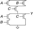
Figure 1.51 Mystery schematic
Exercise 1.89 Implement the following three-input gates using only pseudo-nMOS logic gates. Your gates receive three inputs, A, B, and C. Use a minimum number of transistors.
Exercise 1.90 Resistor-Transistor Logic (RTL) uses nMOS transistors to pull the gate output LOW and a weak resistor to pull the output HIGH when none of the paths to ground are active. A NOT gate built using RTL is shown in Figure 1.52. Sketch a three-input RTL NOR gate. Use a minimum number of transistors.

Figure 1.52 RTL NOT gate
Interview Questions
These questions have been asked at interviews for digital design jobs.
Question 1.1 Sketch a transistor-level circuit for a CMOS four-input NOR gate.
Question 1.2 The king receives 64 gold coins in taxes but has reason to believe that one is counterfeit. He summons you to identify the fake coin. You have a balance that can hold coins on each side. How many times do you need to use the balance to find the lighter, fake coin?
Question 1.3 The professor, the teaching assistant, the digital design student, and the freshman track star need to cross a rickety bridge on a dark night. The bridge is so shaky that only two people can cross at a time. They have only one flashlight among them and the span is too long to throw the flashlight, so somebody must carry it back to the other people. The freshman track star can cross the bridge in 1 minute. The digital design student can cross the bridge in 2 minutes. The teaching assistant can cross the bridge in 5 minutes. The professor always gets distracted and takes 10 minutes to cross the bridge. What is the fastest time to get everyone across the bridge?