

Boolean logic is the basis of computation in modern computer systems. You can represent any algorithm, or any electronic computer circuit, using a system of Boolean equations. To fully understand how software operates you need to understand basic Boolean logic and digital design.
This material is especially important to those who want to design electronic circuits or write software that controls electronic circuits. Even if you never plan to do this, you can use your knowledge of Boolean logic to optimize your software. However, there is one other reason for studying Boolean functions, even if you never intend to do either of these two things. Many high-level languages process Boolean expressions, such as those that control an if statement or while loop. By optimizing your Boolean expressions, it is often possible to improve the performance of high-level language code. Therefore, studying Boolean functions is important even if you never intend to design an electronic circuit. It can help you write better code in a traditional programming language.
Boolean algebra is a deductive mathematical system. A binary operator “°” accepts a pair of Boolean inputs and produces a single Boolean value. For example, the Boolean AND operator accepts two Boolean inputs and produces a single Boolean output (the logical AND of the two inputs).
For our purposes, we will base Boolean algebra on the following set of operators and values:
The two possible values in the Boolean system are zero and one. Often we will call these values false and true, respectively.
The symbol “•” represents the logical AND operation. For example, A • B is the result of logically ANDing the Boolean values A and B. When using single letter variable names, this text will drop the “•” symbol; therefore, AB also represents the logical AND of the variables A and B, which we will also call the product of A and B.
The symbol “+” represents the logical OR operation. For example, A + B is the result of logically ORing the Boolean values A and B. We will also call this the sum of A and B.
Logical complement, logical negation, and NOT, are all names for the same unary operator. This chapter will use the (') symbol to denote logical negation. For example, A' denotes the logical NOT of A.
Every algebraic system follows a certain set of initial assumptions, or postulates. You can deduce additional rules, theorems, and other properties of the system from this basic set of postulates. Boolean algebra systems are no different, and usually employ the following postulates:
Closure. A Boolean system is closed with respect to a particular binary operator if, for every pair of Boolean values, it only produces a Boolean result.
Commutativity. A binary operator “°” is said to be commutative if A ° B = B ° A for all possible Boolean values A and B.
Associativity. A binary operator “°” is said to be associative if (A ° B) ° C = A ° (B ° C) for all Boolean values A, B, and C.
Distribution. Two binary operators “°” and “%” are distributive if A ° (B % C) = (A ° B) % (A ° C) for all Boolean values A, B, and C.
Identity. A Boolean value
Iis said to be the identity element with respect to some binary operator “°” if A ° I = A for all Boolean values A.Inverse. A Boolean value
Iis said to be the inverse element with respect to some binary operator “°” if A ° I = B and B ≠ A (i.e., B is the opposite value of A in a Boolean system) for all Boolean values A and B.
When applied to the Boolean operators, the preceding postulates produce the following set of Boolean postulates:
P1: Boolean algebra is closed under the AND, OR, and NOT operations.
P2: The identity element of AND (•) is one, and the identity element of OR (+) is zero. There is no identity element with respect to logical NOT (').
P3: The • and + operators are commutative.
P4: • and + are distributive with respect to one another. That is, A • (B + C) = (A • B) + (A • C) and A + (B • C) = (A + B) • (A + C).
P5: • and + are both associative. That is, (A • B) • C = A • (B • C) and (A + B) + C = A + (B + C).
P6: For every value A there exists a value A' such that A • A' = 0 and A + A' = 1. This value is the logical complement (or NOT) of A.
You can prove all other theorems in Boolean algebra using this set of Boolean postulates. This chapter will not go into the formal proofs of the following theorems, but familiarity with some important theorems in Boolean algebra will be useful. Here are some of the important theorems:
| Th1: A + A = A |
| Th2: A • A = A |
| Th3: A + 0 = A |
| Th4: A • 1 = A |
| Th5: A • 0 = 0 |
| Th6: A + 1 = 1 |
| Th7: (A + B)' = A' • B' |
| Th8: (A • B)' = A' + B' |
| Th9: A + A • B = A |
| Th10: A • (A + B) = A |
| Th11: A + A'B = A + B |
| Th12: A' • (A + B') = A'B' |
| Th13: AB + AB' = A |
| Th14: (A' + B') • (A' + B) = A' |
| Th15: A + A' = 1 |
| Th16: A • A' = 0 |
Note
Theorems seven and eight are called DeMorgan’s Theorems after the mathematician who discovered them.
An important principle in the Boolean algebra system is that of duality. Each pair, theorems 1 and 2, theorems 3 and 4, and so on, forms a dual. Any valid expression you can create using the postulates and theorems of Boolean algebra remains valid if you interchange the operators and constants appearing in the expression. Specifically, if you exchange the • and + operators and swap the 0 and 1 values in an expression, the resulting expression will obey all the rules of Boolean algebra. This does not mean the dual expression computes the same values; it only means that both expressions are legal in the Boolean algebra system.
If several different Boolean operators appear within a single Boolean expression, the result of the expression depends on the precedence of the operators. The following Boolean operators are ordered from highest precedence to lowest:
The logical AND and OR operators are left associative. This means that if two operators with the same precedence appear between three operands, you must evaluate the expressions from left to right. The logical NOT operation is right associative, although it would produce the same result using either left or right associativity because it is a unary operator having only a single operand.
A Boolean expression is a sequence of zeros, ones, and literals separated by Boolean operators. A Boolean literal is a primed (negated) or unprimed variable name, and all variable names will be a single alphabetic character. A Boolean function is a specific Boolean expression; we will generally give Boolean functions the name F with a possible subscript. For example, consider the following Boolean function:
F0 = AB + C
This function computes the logical AND of A and B and then logically ORs this result with C. If A = 1, B = 0, and C = 1, then F0 returns the value one (1 • 0 + 1 = 1).
You can also represent a Boolean function with a truth table. The truth tables for the logical AND and OR functions are shown in Table 8-1 and Table 8-2.
For binary operators and two input variables, this form of a truth table is very natural and convenient. However, for functions involving more than two variables, these truth-table forms don’t work well.
Table 8-3 shows another way to represent truth tables. This form has several advantages — it is easier to fill in the table, it supports three or more variables, and it provides a compact representation for two or more functions. The example in Table 8-3 demonstrates how to create a truth table for three different functions of three input variables.
Table 8-3. Truth Table Format for a Function of Three Variables
C | B | A | F = ABC | F = AB + C | F = A+BC |
|---|---|---|---|---|---|
0 | 0 | 0 | 0 | 0 | 0 |
0 | 0 | 1 | 0 | 0 | 1 |
0 | 1 | 0 | 0 | 0 | 0 |
0 | 1 | 1 | 0 | 1 | 1 |
1 | 0 | 0 | 0 | 1 | 0 |
1 | 0 | 1 | 0 | 1 | 1 |
1 | 1 | 0 | 0 | 1 | 1 |
1 | 1 | 1 | 1 | 1 | 1 |
Although you can create an infinite variety of Boolean functions, they are not all unique. For example, F = A and F = AA are two different functions. By theorem two, however, it is easy to show that these two functions produce exactly the same result no matter what input value you supply for A. As it turns out, if you fix the number of input variables you’re going to allow, there are a finite number of unique Boolean functions possible. For example, there are only 16 unique Boolean functions with two input variables and there are only 256 possible Boolean functions with three input variables. Given n input variables, there are 22n unique Boolean functions (two raised to two raised to the nth power). With two input variables there are 222 = 24 or 16 different functions. With three input variables there are 223 = 28 or 256 possible functions. Four input variables have 224 or 216, or 65,536 unique Boolean functions.
When working with only 16 Boolean functions (two input variables), we can name each unique function. Table 8-4 lists common names for these functions.
Table 8-4. Common Names for Boolean Functions of Two Variables
Function Number[a] | Function Name | Description |
|---|---|---|
0 | Zero (clear) | Always returns zero regardless of A and B input values |
1 | (NOT (A OR B)) = (A + B)′ | |
2 | Inhibition = AB′ (A AND not B). Also equivalent to A > B or B < A | |
3 | NOT B | Ignores A and returns B′ |
4 | Inhibition (BA′) | Inhibition = BA′ (B AND not A). Also equivalent to B > A or A < B |
5 | NOT A | Returns A′ and ignores B |
6 | Exclusive-or (XOR) | A ⊕ B. Also equivalent to A ≠ B |
7 | (NOT (A AND B)) = (A • B)′ | |
8 | Logical AND | A • B = (A AND B) |
9 | Equivalence (exclusive-NOR) | (A = B). Also known as exclusive-NOR (not exclusive-OR) |
10 | A | Copy A. Returns the value of A and ignores B’s value |
11 | Implication, B implies A | A + B′. (If B then A). Also equivalent to B ≥ A |
12 | B | Copy B. Returns the value of B and ignores A’s value |
13 | Implication, A implies B | B + A′. (If A then B). Also equivalent to A ≥ B |
14 | Logical OR | A + B. Returns A OR B |
15 | One (set) | Always returns one regardless of A and B input values |
[a] See the discussion of function numbers in the next section. | ||
Beyond two input variables, there are too many functions to provide a specific name for each. Therefore, even when we are referring to functions with two input variables, we will refer to the function’s number rather than the function’s name. For example, F8 denotes the logical AND of A and B for a two-input function and F14 denotes the logical OR operation. Of course, for functions with more than two input variables, the question is, “How do we determine a function’s number?” For example, what is the corresponding function number for the function F = AB + C? Computing the answer is easily done by looking at the truth table for the function. If we treat the values for A, B, and C as bits in a binary number with C being the HO bit and A being the LO bit, they produce the binary strings that correspond to numbers in the range zero through seven. Associated with each of these binary strings is the function result, either zero or one. If we construct a binary number by placing the function result of each combination of the A, B, and C input values into the bit position specified by the binary string of the A, B, and C bits, the resulting binary number will be the corresponding function number. If this doesn’t make sense, an example will help clear it up. Consider the truth table for F = AB + C (see Table 8-5).
Note how the input variables C, B, and A combine to form binary number sequences in the range %000..%111 (0..7). If we use these values to denote bit numbers in an 8-bit value (CBA = %111 specifies bit seven, CBA = %110 specifies bit six, and so on), we can determine the function number by placing at each of these bit positions the result of F = AB + C, for the corresponding combination of C, B, and A values:
CBA:           7    6    5    4    3    2    1    0
F = AB + C:    1    1    1    1    1    0    0    0
Now, if we treat this bit string as a binary number, it produces the function number $F8 or 248. We will usually denote function numbers in decimal. This also provides insight into why there are 22n different functions given n input variables: if you have n input variables, there are 2n different variable value combinations, and thus 2n bits in the function’s binary number. If you have m bits, there are 2m different possible arrangements of those bits. Therefore, for n input variables there are m = 2n possible bits and 2m or 22n possible functions.
You can transform one Boolean expression into an equivalent expression by applying the postulates and theorems of Boolean algebra. This is important if you want to convert a given expression to a canonical form (a standardized form) or if you want to minimize the number of literals or terms in an expression. (A literal is a primed or unprimed variable, and a term is a variable or a product [logical AND] of several different literals.) Minimizing the number of literals and terms can be important because electrical circuits often consist of individual components that implement each literal or term. Minimizing the number of literals and terms in an expression allows a circuit designer to use fewer electrical components and, therefore, to reduce the monetary cost of the system.
Unfortunately, there are no fixed rules you can apply to optimize a given expression. Much like constructing mathematical proofs, an individual’s ability to easily do these transformations is usually a function of experience. Nevertheless, a few examples can show the possibilities:
ab + ab' + a'b            =  a(b + b') + a'b             By P4
                          =  a • 1 + a'b                 By P5
                          =  a + a'b                     By Th4
                          =  a + b                       By Th11


(a'b + a'b' + b')`        =  ( a'(b + b') + b')'         By P4
                          =  (a'• 1 + b')'               By P5
                          =  (a' + b')                   By Th4
                          =  ( (ab)' )'                  By Th8
                          =  ab                          By definition of not


b(a + c) + ab' + bc' + c  =  ba + bc + ab' + bc' + c     By P4
                          =  a(b + b') + b(c + c') + c   By P4
                          =  a • 1 + b • 1 + c           By P5
= a + b + c By Th4Because there is a finite number of unique Boolean functions with n input variables, yet an infinite number of possible logic expressions you can construct from a finite number of functions, there is an infinite number of equivalent logic expressions. To help eliminate confusion, logic designers generally specify a Boolean function using a canonical, or standardized, form. For each different Boolean function, we can choose a single canonical representation of that function.
There are several possible ways to define a set of canonical representations for all the possible Boolean functions of n variables. Within each canonical set, there is a single expression that describes each Boolean function in the system, so as long as you only utilize functions from a single canonical set, all of the functions in the set will be unique. We will discuss only two canonical systems in this chapter and employ only the first of the two. The first is the so-called sum of minterms and the second is the product of maxterms. Using the duality principle we can convert between these two.
As mentioned earlier, a term is either a single literal or a product (logical AND) of several different literals. For example, if you have two variables, A and B, there are eight possible terms: A, B, A', B', A'B', A'B, AB', and AB. For three variables we have 26 different terms: A, B, C, A', B', C', A'B', A'B, AB', AB, A'C', A', AC', AC, B'C', B'C, BC', BC, A'B'C', AB'C', ABC', ABC', A'B'C, AB'C, A'BC, and ABC. As you can see, as the number of variables increases, the number of terms increases dramatically. A minterm is a product containing exactly n literals, where n is the number of input variables. For example, the minterms for the two variables A and B are A'B', AB', A'B, and AB. Likewise, the minterms for three variables A, B, and C are A'B'C', AB'C', A'BC', ABC', A'B'C, AB'C, A'BC, and ABC. In general, there are 2n minterms for n variables. The set of possible minterms is very easy to generate because they correspond to the sequence of binary numbers (see Table 8-6).
Table 8-6. Generating Minterms from Binary Numbers
Binary Equivalent (CBA) | Minterm |
|---|---|
000 | A′B′C′ |
001 | AB′C′ |
010 | A′BC′ |
011 | ABC′ |
100 | A′B′C |
101 | AB′C |
110 | A′BC |
111 | ABC |
We can derive the canonical form for any Boolean function using a sum (logical OR) of minterms. Given F248 = AB + C the equivalent canonical form is ABC + A'BC + AB'C + A'B'C + ABC'. Algebraically, we can show that the canonical form is equivalent to AB + C as follows:
ABC + A'BC + AB'C + A'B'C + ABC'  =  BC(A + A') + B'C(A + A') + ABC'     By P4
                                  =  BC • 1 + B'C • 1 + ABC'             By Th15
                                  =  C(B + B') + ABC'                    By P4
                                  =  C + ABC'                            By Th15 & Th4
                                  =  C + AB                              By Th11
Obviously, the canonical form is not the optimal form. On the other hand, there is a big advantage to using the sum of minterms canonical form: it is very easy to generate the truth table for a function from this canonical form. It is also very easy to generate the sum of minterms canonical form equation from the truth table.
To build the truth table from the sum of minterms canonical form, follow these steps:
Convert minterms to binary equivalents by substituting a 1 for unprimed variables and a 0 for primed variables:
F248
= CBA + CBA' + CB'A + CB'A' + C'BA
= 111 + 110 + 101 + 100 + 011
Place the number 1 in the function column for the appropriate minterm entries:
C
B
A
F = AB + C
0
0
0
0
0
1
0
1
0
0
1
1
1
1
0
0
1
1
0
1
1
1
1
0
1
1
1
1
1
Finally, place the number 0 in the function column for the remaining entries:
C
B
A
F = AB + C
0
0
0
0
0
0
1
0
0
1
0
0
0
1
1
1
1
0
0
1
1
0
1
1
1
1
0
1
1
1
1
1
Going in the other direction, generating a logic function from a truth table, is almost as easy. Follow these steps:
Locate all the entries in the truth table with a function result of one. In this table, these are the last five entries. The number of table entries containing ones determines the number of minterms in the canonical equation.
Generate the individual minterms by substituting A, B, or C for ones and A', B', or C' for zeros. In this example, the result of F248 is one when CBA equals 111, 110, 101, 100, or 011. Therefore, F248 = CBA + CBA' + CB'A + CB'A' + C'AB. The last entry in the table contains all ones, so we generate the minterm CBA. The second-to-last entry contains 110, so we generate the minterm CBA'. Likewise, 101 produces CB'A, 100 produces CB'A', and 011 produces C'BA.
The logical OR and logical AND operations are both commutative, so we can rearrange the terms within the minterms as we please, and we can rearrange the minterms within the overall function as we see fit.
This process works equally well for any number of variables, as with the truth table in Table 8-7 for the function F53,504 = ABCD + A'BCD + A'B'CD + A'B'C'D.
Table 8-7. Truth table for F53,504
D | C | B | A | F = ABCD + A'BCD + A'B'CD + A'B'C'D |
|---|---|---|---|---|
0 | 0 | 0 | 0 | 0 |
0 | 0 | 0 | 1 | 0 |
0 | 0 | 1 | 0 | 0 |
0 | 0 | 1 | 1 | 0 |
0 | 1 | 0 | 0 | 0 |
0 | 1 | 0 | 1 | 0 |
0 | 1 | 1 | 0 | 0 |
0 | 1 | 1 | 1 | 0 |
1 | 0 | 0 | 0 | 1 |
1 | 0 | 0 | 1 | 0 |
1 | 0 | 1 | 0 | 0 |
1 | 0 | 1 | 1 | 0 |
1 | 1 | 0 | 0 | 1 |
1 | 1 | 0 | 1 | 0 |
1 | 1 | 1 | 0 | 1 |
1 | 1 | 1 | 1 | 1 |
Perhaps the easiest way to generate the canonical form of a Boolean function is to first generate the truth table for that function and then build the canonical form from the truth table. In fact, we’ll use this technique when converting between the two canonical forms.
It is also a simple matter to generate the sum of minterms canonical form algebraically. Using the distributive law and theorem 15 (A + A' = 1) makes this task easy. Consider F248 = AB + C. This function contains two terms, AB and C, but they are not minterms. We can convert the first term to a sum of minterms as follows:
AB    =  AB • 1            By Th4
      =  AB • (C + C')     By Th 15
      =  ABC + ABC'        By distributive law
      =  CBA + C'BA        By associative law
Similarly, we can convert the second term in F248 to a sum of minterms as follows:
C     =  C • 1                              By Th4
      =  C • (A + A')                       By Th15
      =  CA + CA'                           By distributive law
      =  CA • 1 + CA' • 1                   By Th4
      =  CA • (B + B') + CA' • (B + B')     By Th15
      =  CAB + CAB' + CA'B + CA'B'          By distributive law
      =  CBA + CBA' + CB'A + CB'A'          By associative law
The last step (rearranging the terms) in these two conversions is optional. To obtain the final canonical form for F248 we need only sum the results from these two conversions:
F248    =  (CBA + C'BA) + (CBA + CBA' + CB'A + CB'A')
= CBA + CBA' + CB'A + CB'A' + C'BAAnother canonical form is the products of maxterms. A maxterm is the sum (logical OR) of all input variables, primed or unprimed. For example, consider the following logic function G of three variables in products of maxterms form:
G = (A + B + C) • (A' + B + C) • (A + B' + C)
Like the sum of minterms form, there is exactly one product of maxterms for each possible logic function. Of course, for every product of maxterms form, there is an equivalent sum of minterms form. In fact, the function G in this example is equivalent to the earlier sum of minterms form of F248:
F248 = CBA + CBA' + CB'A + CB'A' + C'BA = AB + C
Generating a truth table from the product of maxterms is no more difficult than building it from the sum of minterms. You use the duality principle to accomplish this. Remember, the duality principle says to swap AND for OR and zeros for ones (and vice versa). Therefore, to build the truth table, you would first swap primed and non-primed literals. In G, this would yield:
G= (A' + B' + C') • (A + B' + C') • (A' + B + C')
The next step is to swap the logical OR and logical AND operators. This produces the following:
G = A'B'C' + AB'C' + A'BC'
Finally, you need to swap all zeros and ones. This means that for each of the maxterms listed above, you need to store zeros into the function column of the truth table, and then fill in the rest of the truth table’s function column with ones. This will place a zero in rows zero, one, and two in the truth table. Filling the remaining entries with ones produces F248.
You can easily convert between these two canonical forms by generating the truth table for one form and working backward from the truth table to produce the other form. Consider the function of two variables, F7 = A + B. The sum of minterms form is F7 = A'B + AB' + AB. The truth table takes the form shown in Table 8-8.
Working backward to get the product of maxterms, we first locate all entries in the truth table that have a zero result. The entry with A and B both equal to zero is the only entry with a zero result. This gives us the first step of G = A' B'. However, we still need to invert all the variables to obtain G = AB. By the duality principle, we also need to swap the logical OR and logical AND operators, obtaining G = A + B. This is the canonical product of maxterms form.
Because there is an infinite variety of Boolean functions of n variables, but only a finite number of them are unique, you might wonder if there is some method that will simplify a given Boolean function to produce the optimal form. Of course, you can always use algebraic transformations to attempt to produce this optimal form, but you are not guaranteed to arrive at the best result. On the other hand, there are two methods that will always reduce a given Boolean function to its optimal form: the map method and the prime implicants method. In this book, we will only cover the map method.
Because an optimal form must exist for any logic function, you may wonder why we don’t use the optimal form for the canonical form. There are two reasons. First, although it is easy to convert between the truth table forms and the canonical form, it is not as easy to generate the optimal form from a truth table. Second, there may be several optimal forms for a single function.
Using the map method to manually optimize Boolean functions is practical only for functions of two, three, or four variables. With care, you can use it for functions of five or six variables, but the map method is cumbersome to use at that point. For more than six variables, attempting map simplifications by hand would not be wise although it’s probably quite reasonable to write a program that uses the map method for seven or more variables.
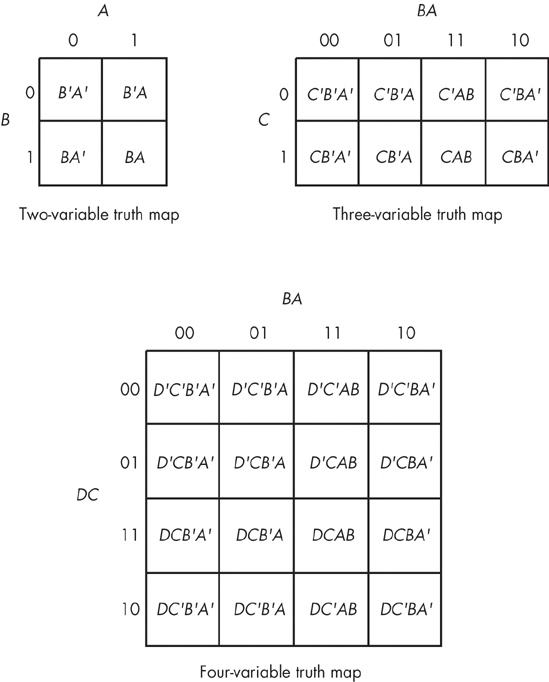
The first step in using the map method is to build a special two-dimensional truth table for the function (see Figure 8-1). Take a careful look at these truth tables. They do not use the same forms appearing earlier in this chapter. In particular, the progression of the 2-bit values is 00, 01, 11, 10, not 00, 01, 10, 11. This is very important! If you organize the truth tables in a binary sequence, the mapping optimization method will not work properly. We will call this a truth map to distinguish it from the standard truth table.
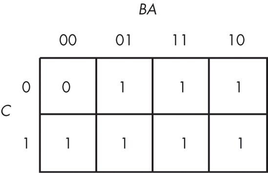
Assuming your Boolean function is already in sum of minterms canonical form, insert ones for each of the truth map cells corresponding to one of the minterms in the function. Place zeros everywhere else. For example, consider the function of three variables F = C'B'A + C'BA' + C'BA + CB'A' + CB'A + CBA' + CBA. Figure 8-2 shows the truth map for this function.
The next step is to draw outlines around rectangular groups of ones. The rectangles you enclose must have sides whose lengths are powers of two. For functions with three variables, the rectangles can have sides whose lengths are one, two, and four. The set of rectangles you draw must surround all cells containing ones in the truth map. The trick is to draw all possible rectangles unless a rectangle would be completely enclosed within another, but at the same time to draw the fewest number of rectangles. Note that the rectangles may overlap as long as one rectangle does not completely enclose the other. In the truth map in Figure 8-3, there are three such rectangles.
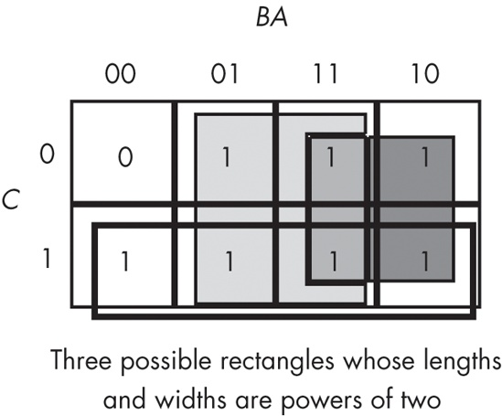
Each rectangle represents a term in the simplified Boolean function. Therefore, the simplified Boolean function will contain only three terms. You build each term using the process of elimination — eliminate any variables whose primed and unprimed forms both appear within the rectangle. Consider the long skinny rectangle in Figure 8-3 that is sitting in the row where C = 1. This rectangle contains both A and B in primed and unprimed forms. Therefore, we can eliminate both A and B from the term. Because the rectangle sits in the C = 1 region, this rectangle represents the single literal C.
Now consider the light gray square in Figure 8-3. This rectangle includes C, C', B, B', and A. Therefore, it represents the single term A. Likewise, the dark gray square in Figure 8-3 contains C, C', A, A', and B. Therefore, it represents the single term B.
The final, optimal, function is the sum (logical OR) of the terms represented by the three squares, or F = A + B + C. You do not have to consider the remaining squares containing zeros.
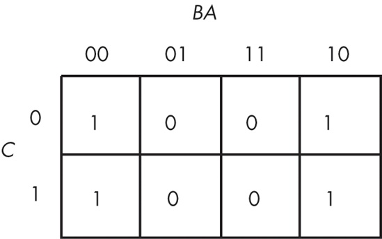
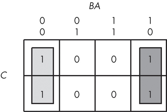
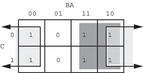
When enclosing groups of ones in the truth map, you must consider the fact that a truth map forms a torus (a doughnut shape). The right edge of the map wraps around to the left edge (and vice versa). Likewise, the top edge wraps around to the bottom edge. This introduces additional possibilities when drawing rectangles around groups of ones in a map. Consider the Boolean function F = C'B'A' + C'BA' + CB'A' + CBA'. Figure 8-4 shows the truth map for this function.
At first glance, you would think that the minimum number of rectangles is two, as shown in Figure 8-5.
However, because the truth map is a continuous object with the right side and left sides connected, we can actually form a single, square rectangle, as Figure 8-6 shows.
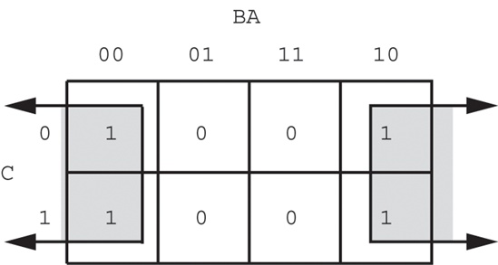
Why do we care if we have one rectangle or two in the truth map? The answer is that the larger the rectangles are, the more terms they will eliminate. The fewer rectangles that we have, the fewer terms will appear in the final Boolean function.
The example in Figure 8-5 with two rectangles generates a function with two terms. The rectangle on the left eliminates the C variable, leaving A'B' as its term. The rectangle on the right also eliminates the C variable, leaving the term BA'. Therefore, this truth map would produce the equation F = A'B' + A'B. We know this is not optimal (see theorem 13).
Now consider the truth map in Figure 8-6. Here we have a single rectangle, so our Boolean function will only have a single term. Obviously, this is better than an equation with two terms. Because this rectangle includes both C and C', and also B and B', the only term left is A'. This Boolean function, therefore, reduces to F = A'.
There are only two types of truth maps that the map method cannot handle properly: a truth map that contains all zeros or a truth map that contains all ones. These two cases correspond to the Boolean functions F = 0 and F = 1 (that is, the function number is zero or 2n − 1). When you see either of these truth maps, you will know how to optimally represent the function.
An important thing to remember when optimizing Boolean functions using the mapping method is that you always want to pick the largest rectangles whose sides’ lengths are powers of two. You must do this even for overlapping rectangles (unless one rectangle encloses another). Consider the Boolean function F = C'B'A' + C'BA' + CB'A' + C'AB + CBA' + CBA. This produces the truth map appearing in Figure 8-7.
The initial temptation is to create one of the sets of rectangles found in Figure 8-8. However, the correct mapping appears in Figure 8-9.
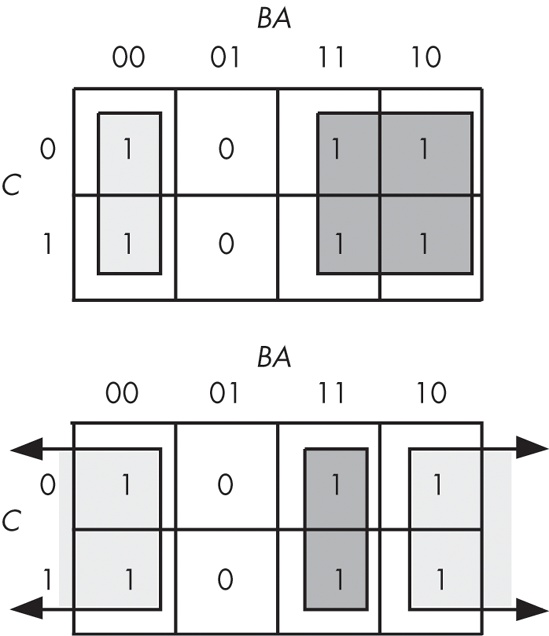
All three mappings will produce a Boolean function with two terms. However, the first two will produce the expressions F = B + A'B' and F = AB + A'. The third form produces F = B + A'. Obviously, this last form is the optimized one (see theorems 11 and 12).
For functions of three variables, the size of the rectangle determines the number of terms it represents:
A rectangle enclosing a single square represents a minterm. The associated term will have three literals.
A rectangle surrounding two squares containing ones represents a term containing two literals.
A rectangle surrounding four squares containing ones represents a term containing a single literal.
A rectangle surrounding eight squares represents the function F = 1.
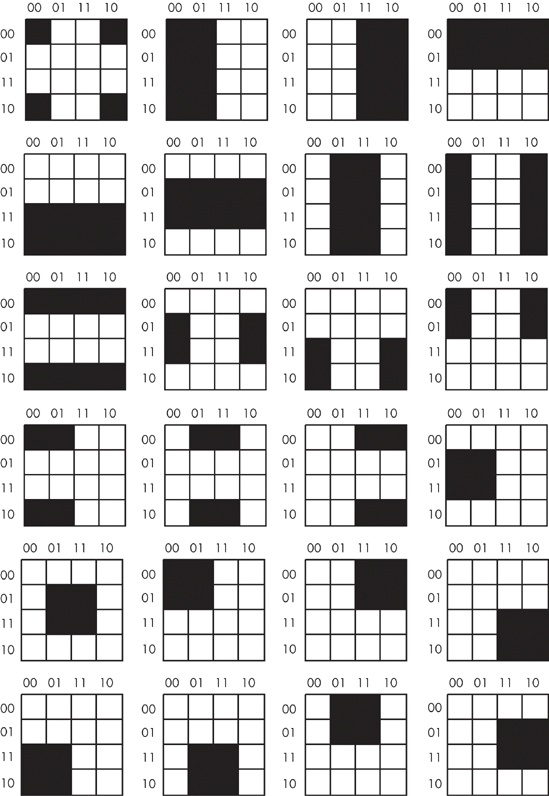
Truth maps you create for functions of four variables are even trickier. This is because there are many places rectangles can hide from you along the edges. Figure 8-10 shows some possible places rectangles can hide.
This list of patterns doesn’t even begin to cover all of them! For example, the diagrams in Figure 8-10 show none of the 1×2 rectangles. You must exercise care when working with four variable maps to ensure you select the largest possible rectangles, especially when overlap occurs. This is particularly important when you have a rectangle next to an edge of the truth map.
As with functions of three variables, the size of the rectangle in a four-variable truth map controls the number of terms it represents.
A rectangle enclosing a single square represents a minterm. The associated term will have four literals.
A rectangle surrounding two squares containing ones represents a term containing three literals.
A rectangle surrounding four squares containing ones represents a term containing two literals.
A rectangle surrounding eight squares containing ones represents a term containing a single literal.
A rectangle surrounding 16 squares represents the function F = 1.
One final example will demonstrate the optimization of a function containing four variables. The function is F = D'C'B'A' + D'C'B'A + D'C'BA + D'C'BA' + D'CB'A + D'CBA + DCB'A + DCBA + DC'B'A' + DC'BA', and the truth map appears in Figure 8-11.
Figure 8-11. Truth map for F = D'C'B'A' + D'C'B'A + D'C'BA + D'C'BA' + D'CB'A + D'CBA + DCB'A + DCBA + DC'B'A' + DC'BA'
Here are two possible sets of maximal rectangles for this function, each producing three terms (see Figure 8-12). Both functions are equivalent; both are optimal (remember, there is no guarantee that there is a unique optimal solution). Either will suffice for our purposes.
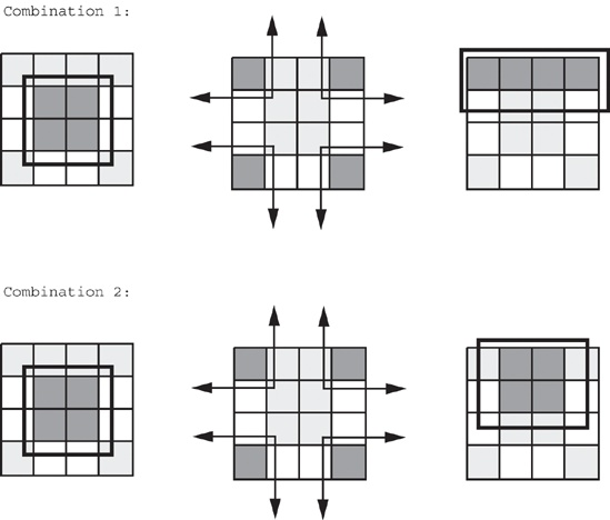
First, let’s consider the term represented by the rectangle formed by the four corners. This rectangle contains B, B', D, and D', so we can eliminate those terms. The remaining terms contained within these rectangles are C' and A', so this rectangle represents the term C'A'.
The second rectangle, common to both maps in Figure 8-12, is the rectangle formed by the middle four squares. This rectangle includes the terms A, B, B', C, D, and D'. Eliminating B, B', D, and D', we obtain CA as the term for this rectangle.
The uppermost of the two combinations in Figure 8-12 has a third term represented by the top row. This term includes the variables A, A', B, B', C' and D'. Because it contains A, A', B, and B', we can eliminate these terms. This leaves the term C'D'. Therefore, the function represented by the upper truth map is F = C'A' + CA + C'D'.
The lower of the two combinations in Figure 8-12 has a third term represented by the top/middle four squares. This rectangle subsumes the variables A, B, B', C, C', and D'. We can eliminate B, B', C, and C' leaving the term AD. Therefore, the function represented by the lower truth map is F = C'A' + CA + AD'.
Although the connection between computer systems and Boolean logic in programming languages like C or Pascal may seem tenuous, it is actually much stronger than it first appears. There is a one-to-one relationship between the set of all Boolean functions and the set of all electronic circuits. Electrical engineers, who design CPUs and other computer-related circuits, have to be intimately familiar with this stuff.
Although the implementation of an algorithm in hardware is well beyond the scope of this book, one important point must be made with respect to such circuitry: Any algorithm you can implement in software, you can also implement directly in hardware. This means that any program you can write, you can also specify as a sequence of Boolean equations.
Of course, it is much easier to specify a solution to a programming problem using languages like Pascal, C, or even assembly language than it is to specify the solution using Boolean equations. Therefore, it is unlikely that you would ever implement an entire program using a set of state machines and other logic circuitry. Nevertheless, there are times when a hardware implementation is better. A hardware solution can be one, two, three, or more orders of magnitude faster than an equivalent software solution. Therefore, some time-critical operations may require a hardware solution.
A more interesting fact is that it is also possible to implement all hardware functions in software. This is important because many operations you would normally implement in hardware are much cheaper to implement using software on a microprocessor. Indeed, one of the primary uses of assembly language on modern systems is to inexpensively replace a complex electronic circuit. It is often possible to replace many tens or hundreds of dollars of electronic components with a single $5 microcomputer chip. The whole field of embedded systems deals with this very problem. Embedded systems are computer systems embedded in other products. For example, most microwave ovens, TV sets, video games, CD players, and other consumer devices contain one or more complete computer systems whose sole purpose is to replace a complex hardware design. Engineers use computers for this purpose because they are less expensive and easier to design with than traditional electronic circuitry.
You can easily design software that reads switches (input variables) and turns on motors, LEDs, or lights, or that locks or unlocks a door. To write such software, you will need an understanding of Boolean functions and of how to implement such functions in software.
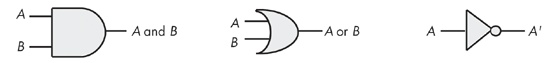
For any Boolean function, you can design an equivalent electronic circuit and vice versa. Because Boolean functions only use the AND, OR, and NOT Boolean operators (these are the only operators that appear within canonical forms), we can construct any electronic circuit using only these three operations. The Boolean AND, OR, and NOT functions correspond to the AND, OR, and inverter (NOT) electronic circuit gates (see Figure 8-13). These symbols are standard electronic symbols appearing in schematic diagrams. (interested readers wanted to learn more about electronic schematic diagrams should check out any book on electronic design).
The lines to the left of each item in Figure 8-13, with the A and B labels, correspond to a logic function input; the line leaving each diagram corresponds to the function’s output.
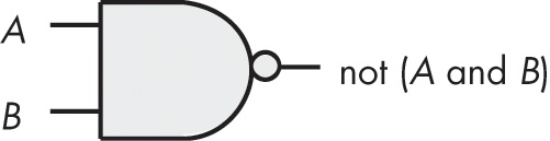
However, you actually need only a single gate type to implement any electronic circuit. This gate is the NAND (not AND) gate, shown in Figure 8-14. The NAND gate tests its two inputs (A and B) and presents a false on the output pin if both inputs are true, it places true on the output pin if both inputs are not true.
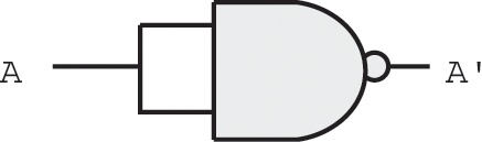
To prove that we can construct any Boolean function using only NAND gates, we must show how to build an inverter (NOT), an AND gate, and an OR gate. Building an inverter is easy; just connect the two inputs together (see Figure 8-15).
Once we can build an inverter, building an AND gate is easy — just invert the output of a NAND gate. After all, NOT (NOT (A AND B)) is equivalent to A AND B (see Figure 8-16). Of course, this takes two NAND gates to construct a single AND gate, but no one said that circuits constructed only with NAND gates would be optimal, only that they would be possible.
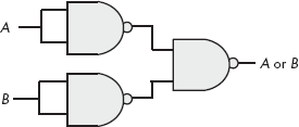
The remaining gate we need to synthesize is the logical-OR gate. We can easily construct an OR gate from NAND gates by applying DeMorgan’s Theorems.
(A or B)'    =    A' and B'            DeMorgan's Theorem.
A or B       =    (A' and B')'         Invert both sides of the equation.
A or B       =    A' nand B'           Definition of NAND operation.
By applying these transformations, you get the circuit in Figure 8-17.
You might be wondering why we would even bother with this. After all, why not just use logical AND, OR, and inverter gates directly? There are two reasons. First, NAND gates are generally less expensive to build than other gates. Second, it is also much easier to build up complex integrated circuits from the same basic building blocks than it is to construct an integrated circuit using different basic gates.
A computer’s CPU is built from combinatorial circuits. A combinatorial circuit is a system containing basic Boolean operations (AND, OR, NOT), some inputs, and a set of outputs. A combinatorial circuit often implements several different Boolean functions, with each output corresponding to an individual logic function. It is very important that you remember that each output represents a different Boolean function.
You can implement addition using Boolean functions. Suppose you have two 1-bit numbers, A and B. You can produce the 1-bit sum and the 1-bit carry of this addition using these two Boolean functions:
S  =  AB' + A'B        Sum of A and B.
C  =  AB               Carry from addition of A and B.
These two Boolean functions implement a half adder. Electrical engineers call it a half adder because it adds two bits together but cannot add in a carry from a previous operation. A full adder adds three 1-bit inputs (two bits plus a carry from a previous addition) and produces two outputs: the sum and the carry. These are the two logic equations for a full adder:
S    =  A'B'Cin + A'BCin' + AB'Cin' + ABCin
Cout  =  AB + ACin + BCin
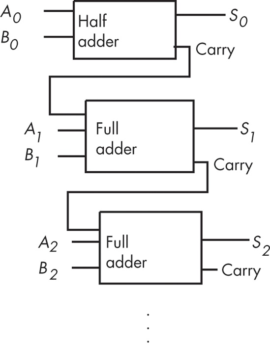
Although these equations only produce a single bit result (plus a carry), it is easy to construct an n-bit sum by combining adder circuits (see Figure 8-18).
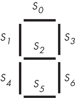
Another common combinatorial circuit is the seven-segment decoder. Decoder circuits are among the more important circuits in computer system design — they provide the ability to recognize (or decode) a string of bits.
The seven-segment decoder circuit accepts an input of four bits and determines which segments to illuminate on a seven-segment LED display. Because a seven-segment display contains seven output values (one for each segment), there will be seven logic functions associated with it (segments zero through six). See Figure 8-19 for the segment assign-ments. Figure 8-20 shows the active segments for each of the ten decimal values.
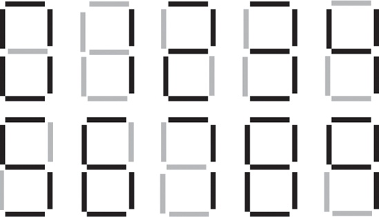
The four inputs to each of these seven Boolean functions are the four bits from a binary number in the range 0..9. Let D be the HO bit of this number and A be the LO bit. Each segment’s logic function should produce a one (segment on) for all binary number inputs that have that segment illuminated in Figure 8-20. For example, S4 (segment four) should be illuminated for numbers zero, two, six, and eight, which correspond to the binary values 0000, 0010, 0110, and 1000. For each of the binary values that illuminates a segment, you will have one minterm in the logic equation:
S4 = D'C'B'A' + D'C'BA' + D'CBA' + DC'B'A'
S0 (segment zero), as a second example, is on for the numbers zero, two, three, five, six, seven, eight, and nine, which correspond to the binary values 0000, 0010, 0011, 0101, 0110, 0111, 1000, and 1001. Therefore, the logic function for S0 is as follows:
S0 = D'C'B'A' + D'C'BA' + D'C'BA + D'CB'A + D'CBA' + D'CBA + DC'B'A' + DC'B'A
A decoder is also commonly used in memory expansion. For example, suppose a system designer wishes to install four (identical) 256-MB memory modules in a system to bring the total to 1 GB of RAM. Each of these 256-MB memory modules has 28 address lines (A0..A27), assuming each memory module is eight bits wide (228 × 8 bits is 256 MB).[33]
Unfortunately, if the system designer hooked up those four memory modules to the CPU’s address bus, each of the modules would respond to the same addresses on the bus. Pandemonium would result. To correct this problem, each memory module needs to respond to a different set of addresses appearing on the address bus. By adding a chip-select line to each of the memory modules, and using a two-input, four-output decoder circuit, we can easily do this. See Figure 8-21 for the details.
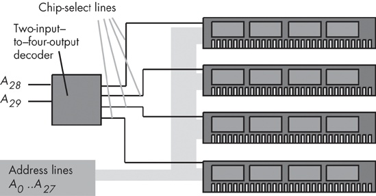
The two-line–to–four-line decoder circuit in Figure 8-21 actually incorporates four different logic functions: one function for each of the outputs. Assuming the inputs are A and B (A = A28 and B = A29), then the four output functions are as follows:
Q0 = A'B'
Q1 = AB'
Q2 = A'B
Q3 = AB
Following standard electronic circuit notation, these equations use Q to denote an output. Also note that most circuit designers use active low logic for decoders and chip enables. This means that they enable a circuit when a low-input value (zero) is supplied and disable the circuit when a high-input value (one) is supplied. In a similar fashion, all the output lines of a decoder chip are normally high, and when the input values A and B select one particular output line, that line goes low. This means that these equations really need to be inverted for real-world examples. We have ignored this issue here and have used positive (or active high) logic.
Decoding circuits are also used to decode machine instructions. We’ll cover this subject in much greater depth in Chapter 9 and Chapter 10, but a simple example is in order here.
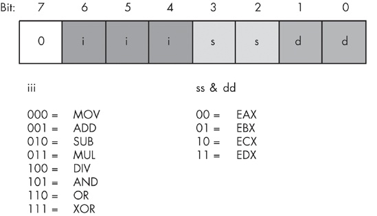
Most modern computer systems represent machine instructions using binary values in memory. To execute an instruction, the CPU fetches the instruction’s binary value from memory, decodes that value using decoder circuitry, and then does the appropriate work. To see how this is done, let’s create a very simple CPU with a very simple instruction set. Figure 8-22 provides the instruction format (all the numeric codes that correspond to the various instructions) for our simple CPU.
Warning
Do not conclude that the instruction format used in this example applies to any particular CPU’s instruction set. The instruction format here is highly simplified to demonstrate instruction decoding.
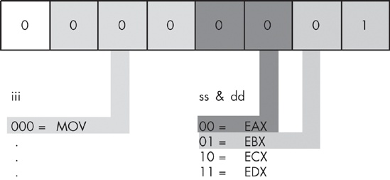
To determine the 8-bit operation code (opcode) for a given instruction, the first thing you do is choose the instruction you want to encode. Let’s pick mov(eax,ebx); as our simple example. To convert this instruction to its numeric equivalent, we follow these steps:
Look up the value for
movin theiiitable in Figure 8-22. The corresponding value is 000, so we must substitute 000 foriiiin the opcode byte.Look up our source operand. The source operand is EAX, whose encoding in the source operand table (
ss&dd) is 00. Therefore, we substitute 00 forssin the instruction opcode.Convert the destination operand to its numeric equivalent. The destination is in EBX, so we look up the value for this operand in the
ss&ddtable. Its value is 01, and we substitute 01 forddin our opcode byte.Assemble these three fields into the opcode byte (a packed data type), to obtain the bit value: %00000001.
Therefore, the numeric value $1 is the value for the mov(eax, ebx); instruction (see Figure 8-23).
Of course, in this example we were actually encoding the instructions. However, the real purpose of this exercise is to discover how the CPU can use a decoder circuit to decode the binary values for machine instructions and execute them at run time. A typical decoder circuit for this example appears in Figure 8-24.
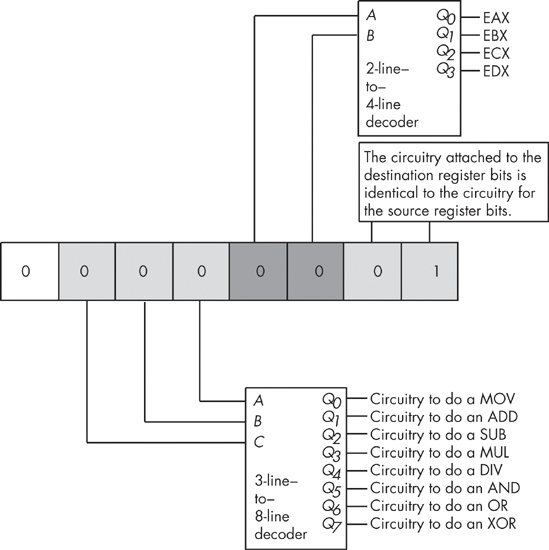
Notice how the circuit in Figure 8-24 uses three separate decoders to decode the individual fields of the opcode. This is much less complex than creating a single 7-line–to–128-line decoder to decode the entire opcode. Of course, all that the circuit in Figure 8-24 will do is tell you which instruction and what operands a given opcode specifies. To actually execute this instruction, you must supply additional circuitry to select the source and destination operands from an array of registers and act accordingly upon those operands. Such circuitry is beyond the scope of this chapter, so we’ll save the juicy details for later.
One major problem with combinatorial logic is that it is memoryless. In theory, all logic function outputs depend only on the current inputs. Any change in the input values immediately appears on the outputs.[34] Unfortunately, computers need the ability to remember the results of past computations. This is the domain of sequential, or clocked, logic.
A memory cell is an electronic circuit that remembers an input value after the removal of that input value. The most basic memory unit is the set/reset flip-flop (S/R flip-flop). You can construct an S/R flip-flop memory cell using two NAND gates, as shown in Figure 8-25. In this diagram, you’ll notice that the outputs of the two NAND gates are recirculated back to one of the inputs of the other NAND gate.
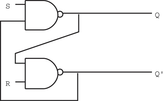
The S and R inputs are normally high, or one. If you toggle the S input by temporarily setting its value to zero and then bringing it back to one, the Q output is set to one. Likewise, if you toggle the R input from one to zero and back to one, this sets the Q output to zero.
Notice that if both S and R are one, then the Q output depends upon the original value of Q itself. That is, whatever Q happens to be, the top NAND gate continues to output that same value. If Q was originally one, then the bottom NAND gate receives two inputs of one (both Q and R), and the bottom NAND gate produces an output of zero (Q'). As a result, the two inputs to the top NAND gate are zero and one, and the top NAND gate produces an output of one, matching the original value for Q.
On the other hand, if the original value of Q was zero, then the inputs to the bottom NAND gate are Q = 0 and R = 1, and the output of this bottom NAND gate is one. As a result, the inputs to the top NAND gate are S = 1 and Q' = 1. This produces a zero output, the original value of Q.
Now suppose Q is zero, S is zero, and R is one. This sets the two inputs to the top NAND gate to one and zero, forcing the output (Q) to one. Returning S to the high state does not change the output at all, because the value of Q' is one. You will obtain this same result if Q is one, S is zero, and R is one. Again, this produces a Q output value of one, and again this value remains one even when S switches from zero to one. To overcome this and produce a Q output of one, you must toggle the S input. The same idea applies to the R input, except that toggling it forces the Q output to zero rather than to one.
There is one catch to this circuit. It does not operate properly if you set both the S and R inputs to zero simultaneously. This forces both the Q and Q' outputs to one (which is logically inconsistent). Whichever input remains zero the longest determines the final state of the flip-flop. A flip-flop operating in this mode is said to be unstable.
Table 8-9 lists all the output configurations for an S/R flip-flop based on the current inputs and the previous output values.
The only problem with the S/R flip-flop is that to be able to remember either a zero or a one value, you must have two different inputs. A memory cell would be more valuable to us if we could specify the data value to remember with one input value and supply a second clock input value to latch the data input value.[35] This type of flip-flop, the D flip-flop (D stands for data) uses the circuit in Figure 8-26.
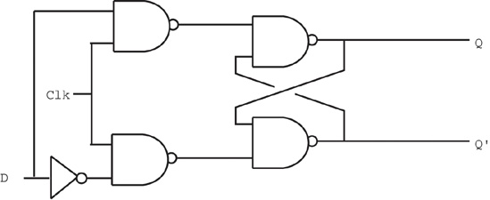
Assuming you fix the Q and Q' outputs to either 0/1 or 1/0, sending a clock pulse that goes from zero to one and back to zero will copy the D input to the Q output (and set Q' to the inverse of Q). To see how this works, just note that the right half of the circuit diagram in Figure 8-26 is an S/R flip-flop. If the data input is one while the clock line is high, this places a zero on the S input of the S/R flip-flop (and a one on the R input). Conversely, if the data input is zero while the clock line is high, this places a zero on the R input (and a one on the S input) of the S/R flip-flop, thus clearing the S/R flip-flop’s output. Whenever the clock input is low, both the S and R input are high, and the outputs of the S/R flip-flop do not change.
Although remembering a single bit is often important, in most computer systems you will want to remember a group of bits. You can do this by combining several D flip-flops in parallel. Concatenating flip-flops to store an n-bit value forms a register. The electronic schematic in Figure 8-27 shows how to build an 8-bit register from a set of D flip-flops.
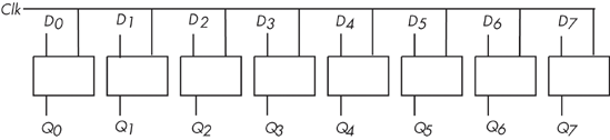
Note that the eight D flip-flops in Figure 8-27 use a common clock line. This diagram does not show the Q' outputs on the flip-flops because they are rarely required in a register.
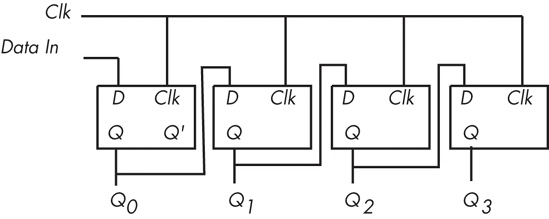
D flip-flops are useful for building many sequential circuits beyond simple registers. For example, you can build a shift register that shifts the bits one position to the left on each clock pulse. A 4-bit shift register appears in Figure 8-28.
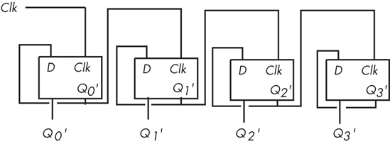
You can even build a counter that counts the number of times the clock toggles from one to zero and back to one using flip-flops. The circuit in Figure 8-29 implements a four bit counter using D flip-flops.
Surprisingly, you can build an entire CPU with combinatorial circuits and only a few additional sequential circuits. For example, you can build a simple state machine known as a sequencer by combining a counter and a decoder, as shown in Figure 8-30.
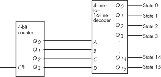
For each cycle of the clock in Figure 8-30, this sequencer activates one of its output lines. Those lines, in turn, may control other circuits. By “firing” those other circuits on each of the 16 output lines of the decoder, we can control the order in which the circuits accomplish their tasks. This is essential in a CPU, as we often need to control the sequence of various operations. For example, it wouldn’t be a good thing if the add(eax,ebx); instruction stored the result into EBX before fetching the source operand from EAX (or EBX). A simple sequencer such as this one can tell the CPU when to fetch the first operand, when to fetch the second operand, when to add them together, and when to store the result away. However, we’re getting a little ahead of ourselves; we’ll discuss this in detail in the next two chapters.
A good understanding of Boolean algebra and digital design is necessary for anyone who wants to understand the internal operation of a CPU. As an added bonus, programmers who understand digital design can write better programs. Although a detailed knowledge of Boolean algebra and digital circuit design isn’t necessary if you simply want to write typical programs, this knowledge will help explain why CPU manufacturers have chosen to implement instructions in certain ways. These questions will undoubtedly arise as we begin to look at the low-level implementation of the CPU.
This chapter is not, by any means, a complete treatment of this subject. If you’re interested in learning more about Boolean algebra and digital circuit design, there are dozens and dozens of books on this subject.
[33] Actually, most memory modules are wider than eight bits, so a real 256-MB memory module will have fewer than 28 address lines, but we will ignore this technicality in this example.
[34] In practice, there is a short propagation delay between a change in the inputs and the corresponding outputs in any electronic implementation of a Boolean function.
[35] “Latch” simply means to remember the value. That is, a D flip-flop is the basic memory element because it can remember one data bit appearing on its D input.