
CHAPTER 8
![]()
Audio Signals and Circuits
Chapters 5 through 7 covered diodes, light-emitting diodes (LEDs), amplifying devices, and operational amplifiers. In particular, we saw on a top level how to use negative feedback with op amps. We will build on some of the circuits and integrate them into more complex circuits. For example, we will show another situation where a constant current source is used for setting the emitter current of a differential transistor amplifier.
A main objective of this chapter is to discuss different types of preamplifiers for microphones and phonograph (phono) cartridges. Note that this chapter will not cover audio power amplifiers, which people have written entire books on.
Signal Levels for Microphones, Phono Cartridges, Line Inputs, and Loudspeakers
Audio signals are measured in terms of root-mean-squared (RMS) voltage or current. A sine-wave signal has a peak voltage, and the peak-to-peak voltage is twice the peak voltage (Figure 8-1).

FIGURE 8-1 Sine-wave signal at 1 volt peak, where the vertical axis is amplitude and the horizontal axis is time.
A sine-wave voltage is not a constant direct-current (DC) voltage. It fluctuates between a positive and a negative voltage, and at times, its voltage is zero. When the power is calculated from the peak sine-wave signal, we actually get half the power. For example, a 10 volt peak sine-wave voltage Vp across a 1 Ω resistor yields a power P = (½)(Vp)2/1 Ω = (½) × 102 watts = 50 watts. In contrast, a 10 volt DC voltage across a 1 Ω resistor yields (10 volts)2/1 Ω = 100 watts.
By Ohm’s law, power is proportional to the square of the voltage or current. So how do we express an equivalent voltage VRMS related to the peak sine-wave voltage Vp that matches the DC voltage in terms of power? That is, can we find an equivalent alternating-current (AC) voltage without the ½ factor that includes (Vp)2 for the power formula P = (½)(Vp)2/R? Let’s come up with a new voltage called VRMS to represent an AC voltage that has the same power as a DC voltage that does not require the ½ factor. Now let’s equate the two power formulas this way:
(VRMS)2/R = P = (½)(Vp)2/R
We can multiply by R on both sides to “solve” for what VRMS is in terms of Vp, which yields
(VRMS)2 = (½)(Vp)2
Now let’s take the square root of both sides:
![]()
Equivalently, we can find Vp in terms of VRMS by multiplying by the ![]() on both sides, which yields
on both sides, which yields
![]()
In an example for a 1 volt peak sine wave, the equivalent RMS voltage:
![]()
In power supplies, the secondary transformer winding voltage may be VRMS = 12 volts AC, which leads to a peak sine-wave voltage of Vp = 12(![]() ) volts peak = 16.9 volts peak.
) volts peak = 16.9 volts peak.
Audio signals can be measured in terms of peak, peak-to-peak, and RMS voltages (or currents). The most common measurement used in meters is the RMS voltage. Table 8-1 lists various audio signal levels.
TABLE 8-1 Various Audio Levels for Audio Devices in RMS AC Voltages
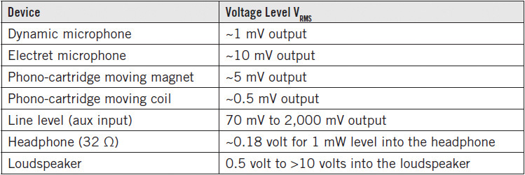
The microphone output levels shown in Table 8-1 are for normal speaking levels. Obviously, placing them in front of musical instruments can result in output levels of over 100 times nominal levels. Moving-magnet phono cartridges, which are the most commonly used types, also can generate output signals on the order of 50 mV to 100 mV depending on the recording. As for line-level audio signals, there are the “old school” devices such as phono preamps, FM tuners, and so on that can generate as low as 70 mV, but today’s CD, DVD, and Blu-Ray players will deliver audio signals on the order of 1 volt to 2 volts.
Balanced or Differential-Mode Audio Signals Used in Broadcast or Recording Studios
Audio signals used in consumer equipment are unbalanced, which means there is a hot and a ground lead. Over long distances, the ground lead, which is supposed to shield again hum or other noise pickup, can itself be induced with noisy signals. To further reduce induced noise pickup over wires, a balanced or differential-mode audio signal can be used.
When audio signals are delivered over long lines such as telephone lines or microphone cables, a balanced or differential-mode signal is outputted, and this signal is received with a balanced or differential amplifier. Noise will be induced or added in a common-mode manner. The balanced audio line has two leads that have equal and opposite audio voltages with respect to ground. Noise is induced equally on both lines but with the phase or polarity as a common-mode noise signal.
To further understand this concept, we can try the following experiment, as shown in Figure 8-2, where we apply a hum signal injected to the common-ground signal while applying a balanced line audio signal. Both the common-mode hum signal and the balanced-mode audio signal are connected to a common amplifier (U1A) that amplifies signals referenced to ground, whereas the balanced-mode amplifier (U1B) only amplifies the signal across the balanced line and rejects the common-mode hum signal that is referenced to ground.

FIGURE 8-2 An experiment with common-mode and balanced audio signals.
This experiment involves connecting a CD or radio headphone output signal to transformer T1 to provide music (or voice) signals. The secondary winding of T1 then has music across pins 5 and 8, the outer terminals. At the center tap of T1, we add a hum signal via T2, an AC adapter, to provide a hum signal on both pins 5 and 8. At the receiving end, there are two different types of amplifiers, a differential-mode (aka balanced-mode) amplifier via U1B and a common-mode (aka unbalanced-mode) amplifier via U1A. The balanced mode only “reads” voltages that are the difference between the two outer terminals of T1. The music signal has a balanced output at T1, so U1B will receive the music signal fine while subtracting out the hum signal that is the same on both terminals at the secondary winding of T1. This subtracting effect accounts for the noise-reducing advantage of using balanced-output and balanced-input amplifiers.
The common-mode amplifier, by summing resistors R8 and R9, will add the hum signal that is applied at the center tap of T1 to be amplified while nulling out the differential-mode music signal. The reason why the differential mode signal is nulled is that the music signal is equal and opposite at pins 5 and 8, the output terminals of T1 referenced to ground. Note that better nulling of the balanced-mode signal can be achieved by replacing R8 and R9 with a 20 kΩ or 50 kΩ potentiometer (pot) where the middle (slider) terminal of the pot is connected to pin 3 of U1A and the outer leads of the pot are connected to pins 5 and 8 of T1. Note that T1, Catalog/Part Number 273-1380, is available at RadioShack.
A common-mode amplifier is not normally used, and this experiment just shows how it can be used. Nevertheless, there have been systems that have both differential- and common-mode signals sent across a balanced pair of wires plus the ground connection. For example, when I worked at a radio station, the audio signal from the studio to the transmitter room was delivered by a pair of balanced audio signal wires. To turn on and off the transmitter from the studio, a common-mode DC signal was supplied to both the balanced audio signal wires (e.g., +24 volts DC) by a center-tap connection of a transformer and ground. The transmitter received the AC audio signal fine via transformers, and the control circuitry sensed whether there was a DC voltage referenced to ground.
Balanced lines are commonly used in broadcast and recording studios. Long runs of wire are prone to pick up noise such as hum. However, most of the noise is common-mode noise, and thus, an audio system with balanced outputs and balanced inputs will reduce this type of noise substantially.
Originally, the balanced outputs and inputs were implemented with transformers, and although they are not used as often today, transformers can be used. It’s more of a question of space and cost. High-quality audio transformers are relatively expensive when compared with a balanced-output or balanced-input amplifier with integrated circuits (ICs).
Typical balanced-output and balanced-input levels for 0 VU on an audio meter vary from 0 dBm to +8 dBm. The level of 0 dBm is 1 mW across a 600 Ω resistor or 0.775 volt RMS. See the VU meter in Figure 8-3. Note that most analog meters include a set screw to adjust the nominal position at zero signal level. This meter is adjusted deliberately slightly to the left side to show more clearly the –20 dB and 0 percent markings.

FIGURE 8-3 An analog VU meter.
We can find out what +8 dBm is in terms of voltage by the following formula. If we call 0 dBm a reference-voltage level at 0.775 volts RMS, then +8 dBm is a multiplying factor |Vout/Vin| of the 0 dBm level. We can express the multiplying factor as follows:
![]()
Thus +8 dB translates to 108 dB/20 dB = 108/20 = 2.51 times over 0 dBm. And thus +8 dBm = 2.51 × 0 dBm = 2.51 × 0.775 volt = 1.945 volts RMS.
Therefore, the range of voltages in a broadcast or recording studio is 0.775 volt to 1.945 volts referenced to 0 VU. By the way, VU stands for “volume unit.” By looking at the VU meter’s marking in decibels (dB) and percentage, we see that –1 dB is about 90 percent, –2 dB is about 80 percent, –3 dB is about 70 percent (it’s actually 70.7 percent), –6 dB is half or 50 percent, and so on. Equation (8-1) gives the exact reading when converting dB (decibels) into a number. For example, +6 dB is 2 or 200 percent. The VU meter shows a relative audio level, and generally, when recording an audio signal, it is useful to keep the meter’s reading above –6 dB (~50 percent) and below +3 dB (~141 percent). There are other standards such as dBV, which has 1 volt RMS at 0 VU instead of 0.775 volt. Using a VU meter does not limit the audio signal to balanced audio signals, and unbalanced signals are often used with equipment having VU meters.
Now let’s take a look at how balanced audio signals are provided and received. Figure 8-4 shows balanced output and input amplifier circuits.
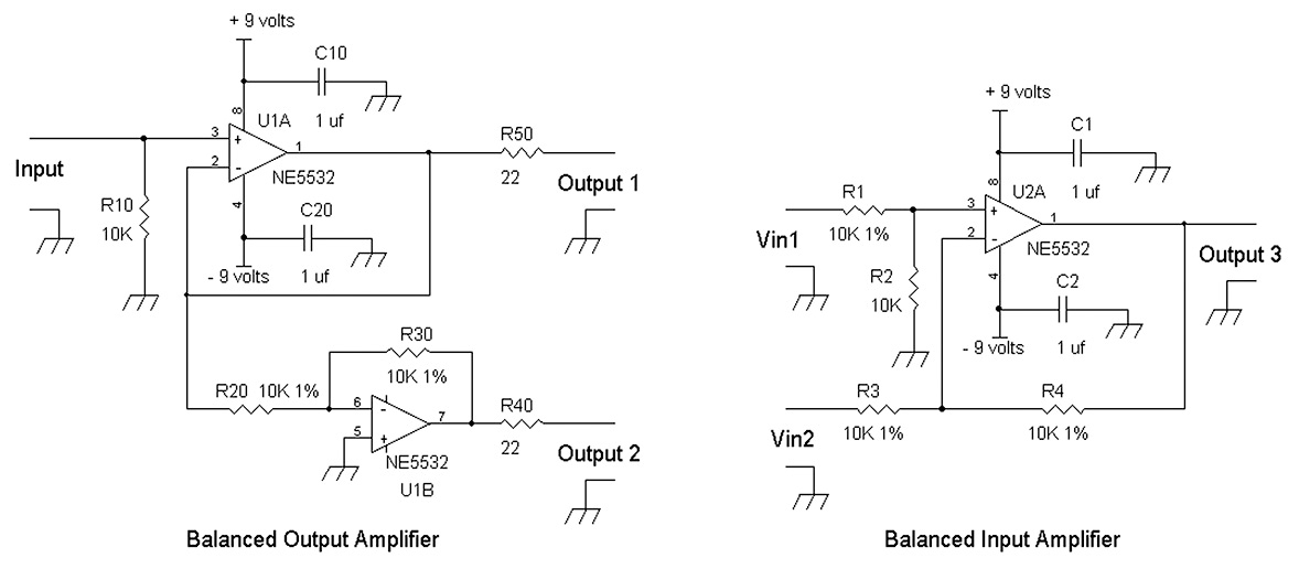
FIGURE 8-4 Balanced audio circuits.
For generating a balanced output signal via the Balanced Output Amplifier in Figure 8-4, connect a unity-gain inverting op amp (U1B) as shown, where R20 = R30, and use a voltage-follower amplifier (U1A). The output voltage across U1A and U1B via Output1 and Output 2 is twice the voltage from the single-ended outputs of either U1A or U1B. Although originally the output resistors for U1A and U1B were set to 300 Ω each to provide a total balanced-output resistance of 600 Ω, by at least the 1980s, the resistor values (e.g., R40 and R50) were kept as low as possible, typically 10 Ω to 22 Ω, which results in a total balanced-output resistance of 20 Ω to 44 Ω. Because of long cable runs throughout the broadcast or recording studio, the capacitance of the cable was substantial and caused a frequency roll-off at 20 kHz with a balanced-output resistance of 600 Ω.
NOTE Be sure to specify an op amp that has sufficient current drive into a 600 Ω load. Most general purpose op amps (e.g., LM1458, TL082, or LF353) have about a 10-mA to 15-mA maximum output, which is not always sufficient. Op amps such as the LM5532, LM833, or OPA2134 are designed to drive 600 Ω loads without problems.
The Balanced Input Amplifier in Figure 8-4 receives a balanced output signal. Thus, Vin1 = –Vin2. In general, this amplifier can be looked at as a combination inverting-gain amplifier for Vin2 and a non-inverting-gain amplifier for Vin1. Voltage divider circuit resistors R1 and R2 are of the same value, so the voltage at the (+) input of U2A is (½)Vin1. We know that the gain of a non-inverting-gain amplifier using an op amp is (1 + R4/R3) from the (+) input of the op amp U2A to Output 3. Therefore, the output voltage (Output 3) due to Vin1 is
(½)Vin1(1 + R4/R3).
With R4 = R3 and R4/R3 = 1, this results in:
(½)Vin1(1 + R4/R3) = (½)Vin1(1 + 1) = Vin1 (at the output of U2A).
The contribution of Vin2 to the output of U2A is Vin2 × (–R4/R3) = –Vin2 because –R4/R3 = –1, the gain of an inverting-gain op amp.
NOTE For a balanced signal connected to Vin1 and Vin2 of the balanced-input amplifier in Figure 8-4, the input resistance at Vin1 is R1 + R2 = 20 kΩ. However, the input resistance at Vin2 is 10 kΩ/1.5 = 6.66 kΩ. Therefore, to provide equal input resistances at Vin1 and Vin2, set R1 = R2 = 3.33 kΩ or R1=R2 = R3/3. This results in a 6.66 kΩ input resistance at Vin1, which matches the input resistance at Vin2.
If we now take both input signals Vin1 and Vin2 into account, we find that the output signal is then:
Vin1 + –Vin2 = Vin1 – Vin2 = Output 3
To provide the highest performance in rejecting common-mode signals, R1, R2, R3, and R4 are typically 1 percent or better tolerance resistors.
Microphone Preamplifier Circuits
From Table 8-1, the relative levels from microphones are on the order of millivolts (mV), which are very low signal voltages. One can build an amplifier with a gain of about 1,000 and amplify the microphone’s signal to the order of about 1 volt. But the question arises what type of low-noise amplifier we will need to amplify the microphone’s signal without adding noise? Generally, a signal-to-noise ratio of >60 dB, which translates to a >1,000:1 (signal-to-noise) ratio, is required to have the amplified signal relatively hiss-free. For 1 mV of signal from the microphone, we need to ensure that the equivalent noise at the input of the microphone preamp is less than 1 mV/1,000 = 1 μV.
But how do we measure the noise? To measure noise for its associated noise voltage, we must always measure noise at the output of a device with a filter. This is because measuring noise without a filter with a specified bandwidth will result in an erroneous figure. Most audio noise measurements use a bandwidth of 20 kHz or less. And it is very common to use an “A” weighting filter, which has about a 10 kHz bandwidth that can be approximated with a 1 kHz high-pass filter and a 11 kHz low-pass filter connected in series. The “A” weighting filter passes signals whose frequencies are generally audible to the human ear. It should be noted that with white noise (e.g., hiss), which is random, the noise voltage is proportional to the square root of the bandwidth, ![]() .
.
Many op amps have input noise density voltage specifications that we can use to determine how much noise is equivalent at the input of the op amp. The noise density voltage Vnd is specified for a bandwidth of 1 Hz, and to figure out the noise voltage for a specified bandwidth, we have
Total noise = noise density voltage × ![]()
where BW = bandwidth in hertz (Hz). Or, in other words:
![]()
Because we choose a 10 kHz bandwidth for an “A” weighting filter:
Total noise = noise density voltage × ![]() =
=
noise density voltage × 100 = Vnd × 100
Low-noise op amps such as the NE5532, LM4562, and AD797 have noise density voltages of about ![]() respectively. For a 10 kHz bandwidth, the noise voltages are 0.45 μV, 0.27 μV, and 0.1 μV for the NE5532, LM4562, and AD797, which results in signal-to-noise ratios for a 1 mV input signal of about 66 dB (2,000), 71 dB (3,700), and 80 dB (10,000). In practice, we may lose one or two dBs (decibels) in noise performance due to noise voltages generated by the gain-setting feedback resistors or even more due to the noise generated by the microphone itself. A balanced microphone preamplifier is shown in Figure 8-5.
respectively. For a 10 kHz bandwidth, the noise voltages are 0.45 μV, 0.27 μV, and 0.1 μV for the NE5532, LM4562, and AD797, which results in signal-to-noise ratios for a 1 mV input signal of about 66 dB (2,000), 71 dB (3,700), and 80 dB (10,000). In practice, we may lose one or two dBs (decibels) in noise performance due to noise voltages generated by the gain-setting feedback resistors or even more due to the noise generated by the microphone itself. A balanced microphone preamplifier is shown in Figure 8-5.

FIGURE 8-5 A balanced microphone preamplifier for XLR connectors.
Although we could use a balanced-input amplifier like the Balanced Input Amplifier shown in Figure 8-4, the input resistors have to be of low value, such as having R1 = R3 = 100 Ω and R2 = R4 = 20 kΩ, with U2A = LM4562 or other lower-noise op amp, for a gain of 46 dB or 200. In most cases, this balance-input microphone amplifier will work fine unless the user needs to adjust the input-loading resistor for the particular microphone.
Generally, if there is a 150 Ω microphone, the load resistance is much higher, such as 800 Ω or so, to avoid overdamping the voice coil in the microphone. Figure 8-5 shows one such balanced microphone preamplifier where the input resistors R1 and R5 that are set nominally to 1 kΩ each can be replaced with resistors with other values for flexibility of input load resistance.
This microphone preamplifier has input load resistors (R1 and R5) that typically allow for a balanced-input resistance of about 2,000 Ω. The preamp consists of two low-noise non-inverting-gain amplifiers U1A and U1B with low-value resistors R3 and R7 to minimize added noise. The two amplifiers U1A and U1B both have a gain of (1 + 20 kΩ/100) or 201. Gain can be adjusted by varying the values of both feedback resistors R4 and R8. Differential (mode) amplifier U2A ensures that common-mode noise is reduced or nulled. Lower-noise op amps can be found that are better in noise density voltage than the LM4562, but as a good compromise in a dual package, this op amp is fine.
Capacitors C1 and C2 provide some RFI (radio-frequency interference) protection, which is generally needed given the high voltage gain of the amplifier. These capacitors roll off the frequency response at RF signals but pass audio signals.
Generally, for a preamplifier such as this, the supply voltages are typically ±12 volts to ±15 volts. This ensures sufficient dynamic range to accommodate the wide range of sound levels that will be encountered. One way to mitigate the large variation in microphone signal levels is to connect the output of this amplifier via C3 and C4 to the peak limiter amplifier that was presented in Figure 7-11.
Microphones for consumer electronics normally do not have balanced-output signal lines and instead have unbalanced outputs including hot and ground leads via the tip and sleeve of the connector. For unbalance microphones, including those with dynamic and electret elements, see Figures 8-6 and 8-7.

FIGURE 8-6 Preamplifier for unbalanced-output microphones that have sleeve and tip connectors.

FIGURE 8-7 Electret condenser microphone preamplifier with biasing circuit at the input Vin.
In Figure 8-6, the preamplifier has an RFI protection circuit via R2 and C1. Loading of the microphone is set by R1, which can be a resistor with a value from about 500 Ω to 2 kΩ depending on the microphone specifications. This preamplifier is split into two stages, with the first stage having a gain of about 34 via feedback resistors R6 and R7. The second stage is an adjustable-gain amplifier via VR1, which allows setting the second-stage amplifier for a gain of between 2 and about 34. By splitting up the gain distribution over two stages, lower GBWP (Gain Bandwidth Product) op amps may be used if desired, but more important, some control from overload is provided in case the microphone input signal is too high.
For a typical dynamic microphone, a gain of 100 to 1,000 is needed, and for electret types, a gain of about 20 to 100 is needed. Note that the electret microphone requires a DC biasing voltage via a resistor at the input (via R1 in Figure 8-7), and this DC biasing circuit is not to be used with dynamic microphones.
To connect a balanced-output microphone with an unbalanced amplifier, simply ground the (–) terminal to the ground shield and connect in the same manner as an unbalanced dynamic microphone. The electret condenser microphone has a built-in field-effect transistor (FET) amplifier that requires powering via a bias resistor with voltages that vary typically from 1.5 volts to 9 volts. Common biasing voltages are 3 volts or 5 volts. In this particular design, we use a regulated 3.3 volt reference via zener diode ZD1. Because the zener diode is a pretty good white noise generator, low-pass filtering is required to remove the white noise plus any power-supply noise. Thus R9 and C7 form a low-pass filter. The microphone signal is AC coupled and level shifted via C2 to provide the microphone signal that will be amplified by U1A. A gain of 34 is provided via feedback resistors R7 and R6, where the non-inverting-gain op amp gain = [1 + R7/R6] = [1 + 3300/100] = [1 + 33] = 34. Electret microphones provide more signal output, and a gain of about 30 dB is sufficient. Depending on the electret microphone’s signal level, R7 may be changed.
When applying resistive negative feedback around an op amp, the frequency response of the amplifier is given by the gain bandwidth product (GBWP) divided by the gain of the system. When referring to bandwidth, we generally are talking about a –3-dB bandwidth, which translates to a drop off in amplitude response of 1/= + 2, or 0.707. Most op amp data sheets will list the GBWP. For example, an LM1458 op amp with a 1-MHz GBWP set for a noninverting gain of 34 will have a –3-dB bandwidth out to 1 MHz/34 = 29 kHz. So, at 29 kHz, the gain is dropped from 34 to 34 × 0.707 = 24 as opposed to a gain of 34 at a lower frequency such as 1 kHz. With audio signals, the bandwidth or frequency response is often stated as the frequency that causes the signal to drop from 100 percent to 70.7 percent. The op amps were chosen for their high gain bandwidth product (GBWP) such that at maximum gain, the frequency response exceeds 20 kHz by at least threefold. For example, in Figure 8-7, an LM4562 has a GBWP of 55 MHz for a –3-dB bandwidth of 55 MHz/34 = 1.6 MHz. One can also use a lower-priced op amp in Figure 8-7, such as the NE5532 (10-MHz GBWP), which results in a –3-dB bandwidth of 10 MHz/34, or approximately 300 kHz.
Increasing GBWP and Achieving Low Noise with Added Transistors
Of course, there are ways to increase the GBWP and provide low-noise performance in a preamplifier circuit by adding low-noise transistors in front of the op amp, as shown in Figure 8-8. U1A, a TL082 op amp ![]() is about four times noisier than an NE5532, which has an input noise density voltage of
is about four times noisier than an NE5532, which has an input noise density voltage of ![]() Note: In general, noise is generally measured at the output when the input is shorted to ground. By adding a pair of low-noise transistors as shown by Q1 and Q2 (2N4401s), the “new” equivalent input noise density of the preamp is less than
Note: In general, noise is generally measured at the output when the input is shorted to ground. By adding a pair of low-noise transistors as shown by Q1 and Q2 (2N4401s), the “new” equivalent input noise density of the preamp is less than ![]() which is about half the noise of an NE5532.
which is about half the noise of an NE5532.

FIGURE 8-8 Added transistors to increase the overall GBWP of an op amp.
NOTE Care must be taken to avoid oscillations that can happen if the feedback resistors R13 and R12 are set for too low of a gain. For example, to avoid oscillation, the gain = [1 + (R13/R12)]≥ 38. If a gain of 40 is desired, then let R12 = 100 Ω and R13 = 3900 Ω.
The circuit in Figure 8-8 can be rather tricky to build, and an oscilloscope should monitor the output to ensure that the output terminal Vout is free of oscillations. Basically, low-noise 2N4401 transistors Q1 and Q2 are biased as a differential amplifier. Are there other low-noise transistors that one can try? Yes, there are other bipolar transistors such as the 2SA1316, which has a different pin-out of ECB (Emitter-Collector-Base) instead of the EBC (Emitter-Base-Collector) of the 2N4401. And it’s possible to use low-noise JFETs such as the LSK170, but values for R9 = 470 Ω and R11 = 1 kΩ probably will have to be divided by about 5 that results in R9 = 100 Ω and R11 = 200 Ω; and the supply voltage set to +24 volts. Also note that in an FET, the source, gate, and drain correspond in the same order to the emitter, base, and collector of a bipolar transistor. When the circuit in Figure 8-8 is powered on, please wait about 60 seconds for the DC operating points to stabilize.
The collector current of Q3 is determined by the turn-on voltage of LED1 (~1.7 volts DC) and R9. The base-emitter junction turn-on voltage of Q3 is about 0.7 volt, so the voltage across R9 is 1.7 volts – 0.7 volt = 1 volt. Therefore, the emitter current of Q3 is 1 volt/R9 = 1 volt/470 Ω ≈ 2 mA, which is also the collector current of Q3. The op amp via R13 will adjust a voltage at pin 1 of U1A such that equal currents of 1 mA each will flow through R7 and R10. With 1 mA of collector current for Q1 and Q2, the (differential) voltage gain from the bases of Q1 and Q2 to load resistors R7 and R10 is about 38. Basically, increasing the current via R9 will increase the gain proportionally. For example, if R9 is decreased from 470 Ω to 235 Ω, the collector currents of Q1 and Q2 will increase from 1 mA to 2 mA, and the resulting gain will increase from 38 to 76.
The actual gain as defined by the differential output voltage at the collectors of Q1 and Q2 referenced to the input signal at the bases of Q1 and Q2 is:
GainQ1_Q2 = [(½) (IEQ3) × R7/0.026 volt] = gmR7
where IEQ3 is the emitter current of Q3 (e.g., approximately 2 mA for R9 = 470 Ω). For example, if IEQ3 = 2 mA and R7 = 1 kΩ:
GainQ1_Q2 = [(½) (2 mA) × 1 kΩ/0.026 volt] = 1 mA(1 kΩ)/0.026 volt = 38.4
With 1 mA of collector current for Q1 and Q2, this results in an added gain of 38 in front of the op amp U1A, and the GBWP → 38 × GBWPop_amp. This means that the 4-MHz GBWP TL082 is now extended to a GBWP of 38 × 4 MHz, or 152 MHz. The only down side with this setup with the extra gain is that we add another stage that has a phase shift that can cause oscillations in a negative-feedback amplifier. To avoid oscillations, the gain set by the feedback resistors R13 and R12 always must be set to higher than gmRL, which is 38 in this case. In this example, the gain is about 1,000 because R13/R12 = 1,000 > 38, so we are safe.
Moving-Magnet or Magnetic High-Output Phono-Cartridge Preamps
Although compact discs (CDs) and other digitally recorded media are used commonly today in the twenty-first century, analog vinyl records still are being manufactured and have a niche following. The two most common speeds for playing back records are 33⅓ rpm and 45 rpm (rpm = revolutions per minute). Much older records that play back at 78 rpm (e.g., 10-inch disks recorded up to the 1960s) or 16⅔ rpm (e.g., children’s records also from the 1960s) are much less common today.
A stereo magnetic phono cartridge has four leads for the right and left channels. They are right hot, left hot, right ground, and left ground, and these four leads are associated with red, white, green, and blue wires, respectively, in the tone arm. Normally, these cartridges track the records at a stylus force between 1 gram and 3 grams. The stereo output cables of a turntable have a RCA connector plug, where the red-marked cable denotes the right channel, and the left channel is marked in white or black.
Frequency Response and Phase for Recording and Playing Records
A typical vinyl long-playing (LP) record has about 20 to 30 minutes of information on each side. In order to optimize playing time and prevent a cartridge’s stylus from mistracking, the record is recorded with an equalization curve that looks like a bass cut and treble boost. That is, the lower-frequency signals at 20 Hz are recorded at a level about 1/10 the level at 1 kHz, and the higher frequency signals at 20 kHz are recorded about 10 times the level at 1 kHz. In general, most music has a frequency spectrum that is attenuated at high frequencies, and the treble boost at the record cutting end is acceptable.
To play back an analog record, a complementary equalization curve must be included such that there is a bass boost and treble cut. To implement the playback equalization curve, there is a roll-off starting at 50 Hz, which levels out at 500 Hz to about 2.12 kHz, where there is a second roll-off at 2.12 kHz. This second roll-off can continue to beyond 20 kHz, but it is not uncommon to have the second roll-off level out at around a frequency of 40 kHz or higher. Figure 8-9 shows the record and playback frequency responses that follow the Recording Industries Association of America (RIAA) curves.
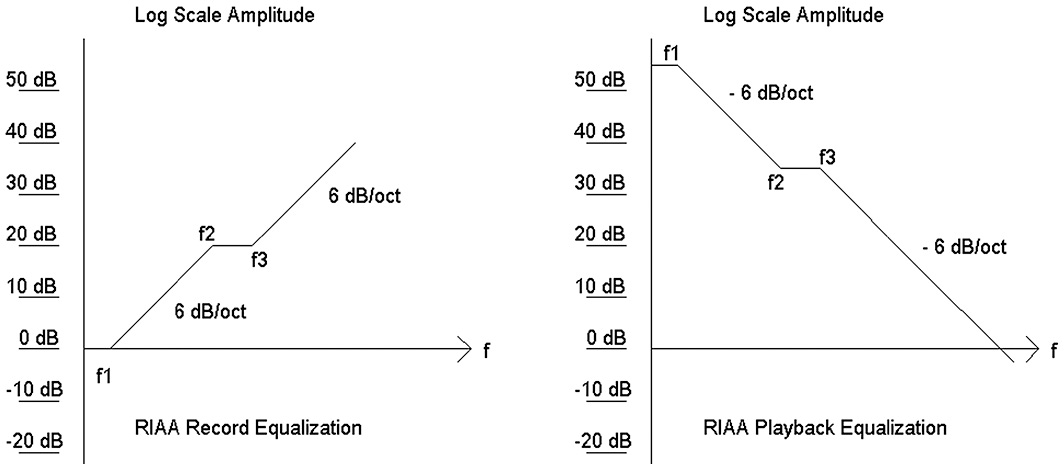
FIGURE 8-9 RIAA record and playback equalization curves for analog vinyl records at 33⅓ and 45 rpm.
In Figure 8-9, we see 6 dB/octave for the RIAA record equalization curve. This means that as the frequency changes by a factor of 2, the 6 dB/octave slope translates to a twofold increase in amplitude. For example, when measuring the amplitude level from the RIAA recording equalization curve at 5 kHz and 10 kHz, the amplitude level at 10 kHz is twice the level of the amplitude at 5 kHz. For a –6 dB/octave slope seen in the RIAA playback equalization curve, the frequency goes up twice, and the amplitude goes down by a factor of ½ (or the reciprocal of 2). For example, in the RIAA playback curve, the signal level at 8 kHz is half the signal level at 4 kHz.
The three frequencies f1, f2, and f3 required to shape the equalization curve can be equivalently stated as time constants. For example, the frequencies f1 = 50 Hz, f2 = 500 Hz, and f3 = 2.12 kHz are equivalently expressed as time constants τ1 = 3,180 μs, τ2 = 318 μs, and τ3 = 75 μs, respectively.
If we choose 50 Hz, for example, we find in an RC low-pass filter that the –3-dB (0.707) cutoff frequency is:
fc = 1/[2τ] = 1/[2RC]
and solving for RC, we will find that τ1 = RC = 3,180 μs = 3,180 × 10–6 second, that is:
50 Hz = 1/[2π(3,180 μs)] = 1/[2π(3,180 × 10–6 second)]
By time constant, we mean that any combination of resistors and capacitors such that the product of their values equal 3,180 μs will provide a cutoff frequency of 50 Hz. For example, combinations of a capacitor of 3,180 pF and a resistor of 1 MΩ or a capacitor of 6,360 pF and resistor of 500 kΩ have the same time constant of 3,180 μs. In this example, doubling the capacitance resulted in halving the resistance.
Three RIAA Equalization Phono Preamplifier Projects
First RIAA Phono Preamp
For the first phono preamplifier project, we will use op amps and active equalization, where the feedback network implements the playback curve entirely (see Figure 8-10).

FIGURE 8-10 A phono preamp using a single op amp per channel.
Parts List
• C1 and C2, 100 pF silver mica or polystyrene capacitors 5% or 10%
• C3, C4, C5, and C7, 1 μF film capacitors (Mylar or polyester) 5% or 10%
• C6 and C8, 100 μF electrolytic capacitors with at least 25 working volts
• C9 and C10, 0.0015 μF polyester, polystyrene, or silver mica 2% tolerance capacitors or use 5% versions measured with a capacitance meter within 2 percent tolerance
• C11, 0.001 μF polyester, polystyrene, or silver mica 1% or 2% tolerance capacitors or use 5% versions measured with a capacitance meter within 2% tolerance
• All resistors ¼ watt unless specified
• R1, 49.9 kΩ, 1% or alternatively 47.5 kΩ, 1%
• R2, 220 Ω, 5%
• R3, 22 Ω
• R4, 1.5 kΩ, 1%
• R5, 1 MΩ, 1% or 5%
• R6, 78.7 kΩ, 1%
• One 8-pin IC socket
• U1, any of the following op amps: LM4562, NE5532, LM833, TL072, TL082, OPA2134, RC4560, RC4558, JRC4556, LF353, or even LM1458
• Batteries or (+) and (–) power supplies from ±9 volts to ±15 volts for +V and –V
This is a non-inverting-gain amplifier with an active equalization feedback network. The feedback network includes two capacitors, C11 (1,000 pF) and the parallel combination of C9 and C10 (3,000 pF), and two resistors, R5 and R6. The gain at 1 kHz is about 52 or approximately 34 dB. The actual circuit analysis of this network to determine the exact values of the time constants is somewhat tedious because there are interactions between the resistors and capacitors.
However, we can make a rough approximation that at low frequencies, R6 at 78.7 kΩ looks relatively low in resistance when compared with R5 at 1 MΩ, so we can say that for low frequencies, R6 is a short circuit in this context. Thus, R5 is now in parallel to C9 and C10, which forms a time constant of 1 MΩ × 3,000 pF = 3,000 μs ≈ 3,180 μs = τ1.
It gets a little more difficult to determine the second time constant, τ2 = 318 μs, because R6 × C9||C10 = 236 μs, so R5 and C11 may be involved with τ2. Obviously, more calculations would be needed, but not in this chapter. I will spare myself and the reader from the long, drawn-out math.
For determining τ3 = 75 μs, we can approximate that the 3,000 pf from C9 and C10 acts like a short circuit by 2.12 kHz and that R5 (1 MΩ) is then in parallel with R6 (78.7 kΩ), which then results in the parallel resistance of R5||R6 = 73 kΩ. From this result, the approximate calculated time constant τ3 = (R5||R6) × C11= 73 kΩ × 1,000 pF = 73 μs ≈ 75 μs.
Well, that’s enough calculations for now. Let’s take a look at the long view of this phono preamp. It has an RFI filter R2 and C2. The load capacitance to the phono cartridge is about 200 pF due to C1 and C2. The 200 Ω for R2 is low enough to connect C2 in parallel with C1. There are two outputs, AC and DC coupled output terminals for Vout1 and Vout2. Either can be used, and Vout1 should be used for line-level preamps with input resistances of at least 10 kΩ. If less low-frequency roll-off is desired, one can increase the capacitance value of C5 to 2.2 μF (nonpolarized electrolytic or film capacitor). A prototype circuit of the first RIAA preamp circuit is shown in Figure 8-11.

FIGURE 8-11 Single op amp per channel RIAA prototype phono preamplifier.
Second RIAA Phono Preamp
A more elaborate phono preamplifier can include passive (R5 and C5) and active equalization (R7, R8, and C9) networks, as shown in Figure 8-12.
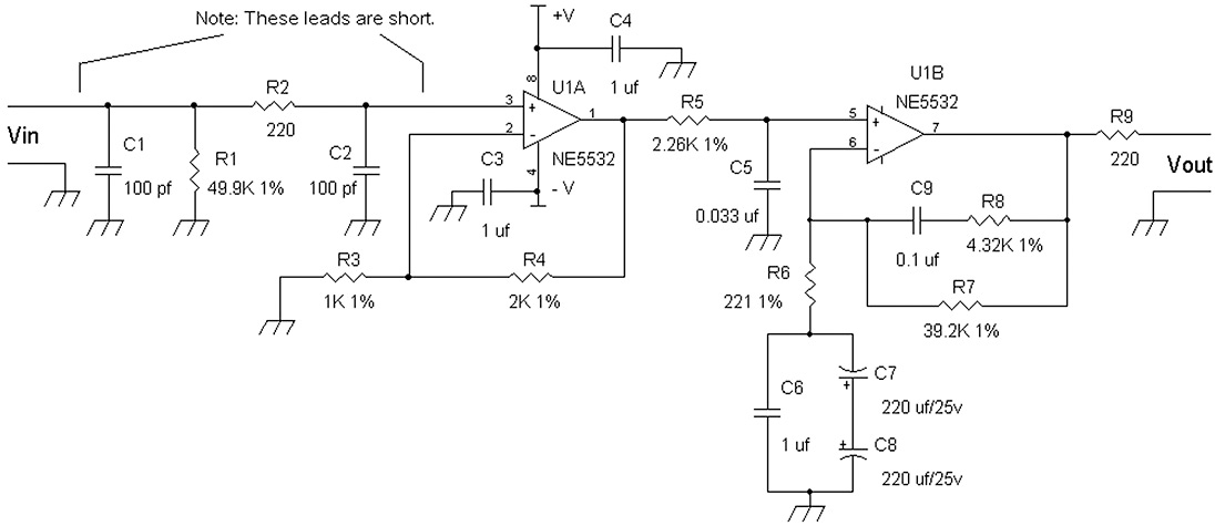
FIGURE 8-12 A phono preamp with active and passive equalization networks.
When I first started designing phono preamps, I used a network similar to the one shown in Figure 8-10. This first preamp was built with a TL072 with an all-in-one active RIAA equalization network; it sounded as good as an audiophile preamp. But then a second high-end preamp was compared with it, and my TL072 preamp lost. So I had to go back to the drawing board. What would I do next to improve the sonic quality (which is always a matter of taste to different listeners)?
Not much time after I designed the TL072 preamp, I thought about implementing the equalization network into two or three stages. By splitting out separate circuits to implement each time constant, possibly a more accurate RIAA playback curve could be achieved. My best estimate was to try to design the new preamplifier in two stages using passive and active RIAA equalization. This was done just before 1980, when I was consulting for an audio cable manufacturer. The challenge at the time was whether I could design a good-sounding do-it-yourself (DIY) preamp for less than $10, not counting the chassis or power supply. I used 9-volt batteries for my tests, which are great temporary “no hum” power supplies.
After building and listening to my first attempt on a passive and active RIAA equalization phono preamp, I was not happy with the sound. But maybe this preamplifier just did not “mate” well with my system but would sound better with another one. I tried out this preamplifier with a different stereo system (different power amplifier and speakers), and everyone liked it because it matched the second high-end preamplifier in sound quality.
The current design shown in Figure 8-12 is actually not the original design from over 30 years ago, but it has many aspects of the original. To ensure buffering and some gain, U1A has a gain of 3 that then drives R5 and C5 for the 75-μs time constant low-pass filter. Equalization has the τ3 75-μs time constant circuit implemented first via R5 and C5, which are 2.26 kΩ and 0.033 μF. Thus, R5 × C5 = 2.26 kΩ × 0.033 μF = 74.6 μs ≈ 75 μs. Also, we can see that a –6 dB/octave slope frequency-response curve is achieved by a simple RC low-pass filter via R5 and C5.
Later on, via U1B, the RIAA equalization with the first two time constants τ1 and τ2 was implemented. We have for τ1 the 3,180-μs time constant provided by R7 (39.2 kΩ) and C9 (0.082 μF) as part of the feedback network in the amplifier with U1B, where the resulting time constant is 3,210 μs ≈ 3,180 μs (within about 1 percent).
The τ2 318-μs time constant is formed by the parallel combination of R7 (39.2 kΩ) and R8 (4.32 kΩ) and C9 (0.082 μF), which results in 3.89 kΩ × 0.082 μF = 319 μs ≈ 318 μs—pretty close! This circuit using R7, C9, and R8 forms a –6 dB/octave slope starting at 50 Hz, and the –6 dB/octave slopes ends a decade later at 500 Hz.
Beyond 500 Hz, the amplitude response levels off to a gain of:
[1 + R8/R6] = [1 + 4.32 kΩ/221 Ω] = 20.5
Intuitively, R7 and C9 start the 3,180-μs time constant 50 Hz roll-off, and eventually, at higher frequencies, R9 is not as relevant, and the second time constant 318 μs is “sort of” formed by C9 and R8. But the exact calculation with the math shows that the 318 μs time constant is really implemented by C9 and R8||R9. Eventually, at higher frequencies, C9 becomes an AC short circuit, and we are left with a straight-gain amplifier determined by R8 and R6. The large-valued capacitors C7 and C8 were designed to be essentially an AC short circuit starting from 20 Hz and beyond. Figure 8-13 shows the preamplifier.

FIGURE 8-13 Prototype circuit of the active and passive RIAA equalization phono preamplifier.
Parts List
• C1 and C2, 100 pF silver mica capacitors 5% or better tolerance
• C3, C4, and C6, 1 μF film capacitors (Mylar or polyester) 10% or better tolerance
• C5, 0.0033 μF film capacitor (Mylar, polyester, or polystyrene) (these should be measured with a capacitance meter to within 2% tolerance)
• C7 and C8, 220 μF electrolytic capacitors with at least 25 working volts rating
• C9, 0.082 μF film capacitor (Mylar, polyester, or polystyrene) (this should be measured with a capacitance meter to within 2% tolerance)
• All resistors ¼ watt unless specified
• R1, 49.9 kΩ or 47.5 kΩ, 1% resistor
• R2, 220 Ω, 5% or 221 Ω, 1% resistor
• R3, 1 kΩ, 1% resistor
• R4, 2 kΩ or 2.21 Ω, 1% resistor
• R5, 2.26 kΩ or 2.21 kΩ, 1% resistor
• R6, 221 Ω, 1% resistor
• R7, 39.2 kΩ, 1% resistor
• R8, 4.32 kΩ, 1% resistor
• R9, 220 Ω, 5% or 221 Ω 1% resistor
• One eight-pin IC socket
• U1A and U1B, one of any of the following dual op amps: LM4562, NE5532, LM833, OPA2134, TL072, TL082, LF353, RC4556, RC4558, RC4560, JRC 4580, or AD712
• Batteries or (+) and (–) power supplies from ±9 volts to ±15 volts for +V and –V
Third Phono Preamplifier: Less Is More?
Simplicity sometimes works just as well in electronic designs. Op amps contain many more transistors than a discrete amplifier design. For example, a phono preamp can be built with just two or three amplifying devices (e.g., tubes, FETs, and/or transistors). When I was designing phono preamps years ago, I found that some of the simplest designs based on fewer amplifying devices in the signal path had good sonic performance. Also, with one of these designs, I can introduce the reader to how amplifiers are designed on the transistor level. We will look at a two-transistor design that was adapted from vacuum-tube phono preamplifiers and redesign it by having an input bipolar transistor followed by a MOSFET output transistor. This can be powered by an 18 volt power supply or by batteries (Figure 8-14).

FIGURE 8-14 Two-transistor phono preamplifier circuit.
Parts List
• C1 and C2, 100 pF silver mica capacitors 5% or better tolerance
• C3, C11, and C12, 10 μF electrolytic capacitors with at least 25 working volts
• C4 and C8, 1,000 μF electrolytic capacitors with at least 35 working volts
• C5 and C6, 0.0015 μF film capacitors (Mylar, polyester, or polystyrene) measured for 2% tolerance with a capacitance meter
• C7, 0.001 μF capacitor (Mylar, polyester, or polystyrene) measured for 2% tolerance with a capacitance meter
• C9, 1 μF film capacitor (Mylar or polyester) with 10% or better tolerance
• Q1 2N3904 or 2N4124 NPN transistor
• Q2 2N7000 N channel MOSFET
• All resistors ¼ watt unless specified
• R1 and R12, 220 Ω, 5% resistor
• R2 and R11, 3.32 kΩ, 1% resistor
• R3, 47 Ω, 5% resistor
• R4, 56.2 kΩ, 1% resistor
• R5, 1.5 kΩ, 1% resistor
• R6, 150 kΩ, 1% resistor
• R7, 825 Ω, 1% resistor
• R8, 75 Ω, 1% resistor
• R9, 1.5 MΩ, 1% or 5% resistor
• Batteries or positive voltage power supply for +18 volts
Although we only have a bipolar transistor Q1 and MOSFET Q2, there’s a lot going on here. Q1 and Q2 form a two-stage amplifier, and the base of Q1 can be considered a (+) input terminal of a feedback amplifier, while its emitter can be considered the (–) input terminal. Although Q1 is not strictly a differential amplifier like Q1 and Q2 in the microphone preamplifier of Figure 8-8, nevertheless, Q1 in Figure 8-14 constitutes a differential amplifier of some sort. The RIAA equalization curve is implemented by using almost the same RIAA network used in Figure 8-10. All the values are the same except that the 1-MΩ resistor is replaced with a 1.5-MΩ resistor because the open-loop gain or composite gain from Q1 to Q2 is only about 2,000 (66 dB), whereas in an op amp, the low-frequency gain is usually greater than 10,000 (>80 dB). R9 is set to the higher value of 1.5 MΩ to ensure that the 3,180-μs time constant is implemented. Generally, when an RIAA preamplifier is built with discrete components and limited low-frequency gain, a resistor such as R9 has to be increased to ensure that at 50 Hz there is sufficient “boost” relative to 1 kHz.
Note that the DC bias drain current of Q7 is set up by having R4 bias the base of Q1. Because the collector current is very low at Q1, about 100 μA, this also leads to very low base current that flows through R5. Thus, the voltage across R5 << VBEQ1 = 0.7 volt. We can estimate that the base voltage reference to ground for Q1 is about 0.7 volt. Thus, the voltage at the source of Q2 is “servoed” to the DC base voltage of Q1 at 0.7 volt. The 0.7 volt DC across the 75 Ω source resistor R8 then sets up a source current of about 0.7 volt/75 Ω ≈ 10 mA. The 10-mA source current sets up a drain current of also 10 mA, and thus 10 mA is flowing through R7. The voltage across R7 is then 825 Ω × 10 mA = 8.25 volts. And thus the voltage at the drain of Q1 is the supply voltage, 18 volts, minus 8.25 volts, which is about 10 volts.
Indeed, there are quite a few things going on with just these two transistors. First, there is a DC bias servo system via R4, and second, there is an AC feedback amplifier that mimics an op amp via the output drain of Q2 and C10 coupled to an RIAA equalization network, which is connected to the (–) input at the emitter of Q1.
The gain of the Q1 first stage is approximately –R6/R5, and the gain of the Q2 second stage is about –gmQ2 × R7. Thus the gain of the Q1and Q2 two-stage amplifier is approximately (R6/R5)gmQ2 × R7, where R7 = 825 Ω. Note: Two negative numbers multiplied result in a positive number. The transconductance of Q2, gmQ2, is the ratio of the output drain to the input (AC) voltage applied to the gate and source. FETs have varied transconductance figures even among the same part number. For this preamplifier, we just measure the voltage gain of Q2. By direct measurement using a low-frequency signal of about 100 Hz, gmQ2 × R7, the gain from the gate to drain of Q2 was found to be about 20. Therefore, the total gain from the base of Q1 to the drain of Q2 is about (150 kΩ/1.5 kΩ)20 ≈ 2,000.
This preamplifier also includes a 3.32 kΩ shelving resistor, R11, to level off the roll-off after 20 kHz at about 45 kHz. This causes a slight boost of 20 kHz, which should not matter much in the tonal playback of a vinyl record. A shelving resistor in series with the RIAA equalization network (C5, C6, C7, R9, and R10) allows for improved stability of the feedback amplifier in terms of preventing oscillation by having the feedback amplifier level off to a gain of [1 + (3.32 kΩ/1.5 kΩ)] = 3.2 instead of unity.
There is a very important note for any two- or three-transistor design similar to this. This pertains to the source (or emitter if Q2 has a bipolar transistor instead of an FET) of the second transistor being fed back to the base of the first transistor via a resistor (e.g., R4). The input resistor R2 is usually on the order of 1 kΩ or more to prevent a low-frequency oscillation from occurring when the phono cartridge is connected to the input terminal Vin. Some phono cartridges have DC resistances of less than 100 Ω, and if R2 → 0 Ω, then input capacitor C3 is essentially connected to ground (DC or low-frequency–wise). A motor-boating oscillation will occur due to a low-frequency phase shift provided by C8 and another low-frequency shift by C3 and R4, the input capacitor. By adding a series resistor R2 (3.32 kΩ) with the input capacitor C3, the low-frequency shift by R4 and C3 is reduced or canceled, and the oscillation is stopped. Recall that it takes at least two stages of phase shift to cause an oscillation. By adding series resistor R2, only one stage of phase shift via C8 remains. Figure 8-15 shows a prototype circuit of the two transistor phono preamplifiers.

FIGURE 8-15 A two-transistor phono preamplifier using a BJT and MOSFET.
Having Fun with Low-Voltage Tube Amplifiers
Before closing out this section on preamplifiers, I want to experiment with using vacuum tubes with just +24 volts for the plates (Figure 8-16). This circuit was built on a Dynaco PAS-3 preamplifier PC-5 circuit board, which is also available on eBay. Also, one can build this circuit on the PC-6 circuit board or just purchase the PC-5 and/or PC-6 fully assembled from eBay and modify the plate, cathode, and feedback resistors. The Dynaco PAS-2 or PAS-3 preamplifier service manual and schematic are available on the Web. One link that has it is www.the-planet.org/dynaco/Preamplifier/PAS2_3.pdf.

FIGURE 8-16 A two-stage triode line amplifier.
NOTE We will not be using the original high-voltage supply power from the original chassis. A suggested +24 volt power supply and filament supply will be shown later in this chapter.
If you are really into modifying tube Dynaco preamplifiers or power amplifiers, see the following links:
• http://curcioaudio.com/index.htm
• http://curcioaudio.com/pasdes_3.htm
Now let’s take a look at working with low-voltage tube line amplifiers. Although the tube specified in the schematic shows a nine-pin 12AU7, other tubes such as the 12BH7, 12U7, and 12FQ7/12CG7 may be used. The gain is set for 11 via resistors R6 and R2. However, because the open-loop gain is not large, the actual gain is about 7 for |Vout/Vin|. Maximum peak-to-peak output voltage is about 5 volts to 8 volts. The 12U7 is a special “space charge” low-voltage tube that works very well. However, it was found that the 12BH7 actually slightly outperformed the 12U7 in terms of maximum output swing given the circuit in Figure 8-16. Other 9-pin 12 volt filament twin triodes such as the 12AT7 and 12AX7 were tried but will produce less voltage swing with the fixed-load resistors R3 at 62 kΩ and R7 at 18 kΩ. Other load resistor values may be tried to optimize the gain and output-voltage swing. Figure 8-17 shows two PAS-3 preamplifier boards available on the Web, such as eBay.
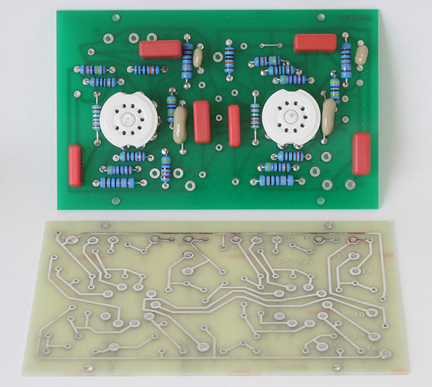
FIGURE 8-17 Assembled PC-6A phono preamplifier and blank PC-5A line amplifier boards.
Power Supplies for the Preamplifier Circuits
In Figures 5-29 and 6-15, two designs of a ±12 volt regulated supply were shown. An improvement was made in ripple rejection by replacing the resistor in Figure 5-29 with the current sources in Figure 6-15. In this chapter, we will show a further improvement to the regulator design simply by using integrated circuit positive and negative voltage regulators 7812T and 7912T (see Figure 8-18).

FIGURE 8-18 A ±12 volt supply using 7812T and 7912T voltage regulator ICs.
The zener diodes and current-source transistors from Figure 6-15 in the previous design have been replaced with voltage-regulator chips. An improvement in the current design (Figure 8-18) has the regulator chips drain less current on standby. Also, the maximum output supply current is good up to 1 amp, provided that the 7812T (U1) and 7912T (U2) chips are mounted on heat sinks.
The previous design with the zener diodes had a maximum supply current of about 40 mA to 50 mA. Note that the pin-outs are different for the negative voltage regulator (7912T pin 1 = ground, pin 2 and tab = input, and pin 3 = output) versus the positive voltage regulator (7812T pin 1 = input, pin 2 and tab = ground, and pin 3 = output). Note also that the middle leads of both chips are connected to the metal tab of the TO220 case. Therefore, although the tab of the 7812 or 7800 Series chips can be mounted directly on a heat sink, the 7900 Series or 7912T voltage regulator cannot be mounted on the same heat sink unless an insulating mounting kit is used to isolate the tab electrically from the heat sink. The power-supply rejection is much better than with the previous designs using the zener diodes. C3 and C4 are positioned very close to the input and ground pins of U1 and U2 so that there is very good input decoupling to avoid instability or oscillations from the voltage regulators.
Note that if the transformer T1 has a 16 volt AC secondary winding, one can replace U1 and U2 with 7815T and 7915T for regulated ±15 volts, or replace U1 and U2 with 7818T and 7918T for a ±18 volt supply. For voltage-regulator chips of this type, the raw DC power-supply voltage connected to the input terminal of the regulator must be at least 2 volts above the regulated output voltage. For example, a 7812T for a +12 volt regulated output should have at least 14 volts at its input terminal. Similarly, a negative voltage regulator such as a 7912T that provides a regulated –12 volts should have at least a negative voltage of –14 volts (e.g., –14 volts DC or less such as –14 volts to –20 volts DC).
In Figure 8-19, one important note to remember is to place the input of U1 near C1 for proper decoupling at the input of the regulator IC. Otherwise, connect a 0.1 μF to 1 μF capacitor close with short leads to the input and ground terminals of U1. This supply can be used to power the two-transistor phono preamplifier.

FIGURE 8-19 A +18 volt power supply for Figure 8-14.
Figures 8-20 and 8-21 can be used for the low-voltage tube line amplifier experiments pertaining to Figure 8-16. There is 24 volts DC to power the filaments of two tubes in series and the plates. Note: A regulated DC source powers the filaments of the tube line amplifier to reduce power supply hum. If AC powered the filaments, then most likely there will be hum at the output of Figure 8-16. Figure 8-20 uses a DC restoration circuit to achieve a voltage doubling effect. C1 and CR1 form a DC restoration circuit to “clamp” the negative peak of the 12 volt AC signal to near zero or ground voltage. The peak voltage from a 12 volt AC RMS source is 12 = + 2 volts = 16.9 volts peak. The peak-to-peak voltage is twice the peak voltage, or about 33.8 volts peak to peak. Thus the waveform at the cathode of CR1 is a varying voltage from about 0 volt to +33.8 volts. The second diode CR2 delivers a peak voltage of +33.8 volts to C2. With its storing capacity, C2 holds the +33.8 volts DC and provides this stored voltage as the raw DC voltage into the 24 volt regulator U1 (7824T). Of course, there are some diode voltage losses in CR1 and CR2 of about 1.5 volts or so, and thus C2 actually would receive about 32 volts instead of 33.8 volts. Again, U1 should be located close to C2, or connect a small capacitor with short leads to the input and ground terminals of U1. Now let’s look at Figure 8-21.

FIGURE 8-20 A +24 volt supply using a DC restoration voltage doubler circuit.

FIGURE 8-21 An alternate power-supply circuit for +24 volts.
A variation of the two half-wave rectifier circuits that provide a plus and minus supply is used here as a voltage-doubler circuit. Originally, the bottom lead of the secondary winding, pin 8, was grounded. But because we can float the lead and ground the anode of CR1 instead, we create approximately referenced to ground a +33 volt raw supply at the cathode of CR2. Basically, C1 and C2 are connected in series. Each capacitor delivers about 16.5 volts DC across C1 and C2, and in series, as shown in Figure 8-21, we get the 33 volts.
Standard Distortion Tests for Audio Equipment
Audio amplifiers are generally tested with sine-wave signals. Ideally, a sine-wave generator provides a signal of a single frequency. When the sine-wave signal is fed to an amplifier, usually some form of distortion occurs at its output. For example, when a 1 kHz tone is fed to the amplifier, the output of the amplifier will show an amplified version of the 1 kHz tone but will also have at its output smaller signals at 2 kHz, 3 kHz, and so on. These signals, which are multiples of the test-tone frequency, are harmonics. For example, the second harmonic of the fundamental frequency signal at 1 kHz is 2 kHz, and the third harmonic is 3 kHz.
In general, to measure an individual nth harmonic distortion, it is HDn = amplitude of the nth harmonic signal/amplitude of the fundamental frequency signal. Put in another way the nth harmonic distortion, HDn, is the ratio of the amplitude of the nth harmonic signal to the amplitude of the fundamental frequency signal.
Total harmonic distortion (THD) is defined as:
THD = [(HD2)2 + (HD3)2 +…+ (HDn)2]1/2
Total harmonic distortion is the result of taking the square root of the sum of the squares of all the harmonic distortions. Fortunately, normally we do not calculate the THD, and there are machines or test equipment to come up with this number. In general, we test the amplifier for THD over a range of 20 Hz to 20 kHz at various output levels. The standard for what constitutes a good number for THD depends on the application. For example, in communication systems such as a voice channel in a two-way radio system, audio THD in the range of less than 3 percent to 10 percent is considered acceptable.
In high-fidelity systems, audio amplifiers generally will have a THD of less than 1 percent, and many will do much better than that—typically less than 0.1 percent. Super-low-distortion amplifiers have distortion levels well below 0.01 percent and sometimes typically less than 0.001 percent, such as the LM4562 op amp when configured for voltage gains of less than 10.
So what causes harmonic distortion? A root cause of this type of distortion is a change in gain of the amplifier for different operating points of the transistors inside the amplifier. We found in Chapter 6 that we could make a voltage-controlled amplifier with a simple common emitter amplifier with its emitter AC grounded by changing the collector current. So any amplifier that has a gain variation due to changes in collector or drain current usually causes harmonic distortion. Other causes of harmonic distortion include voltage-controlled capacitances within the amplifier. These voltage-controlled capacitances are always present in all transistors, JFETs, and MOSFETs.
Let’s introduce a signal that leads into the next type of standard audio test signal, the two-tone test to measure intermodulation distortion (see Figure 8-22).
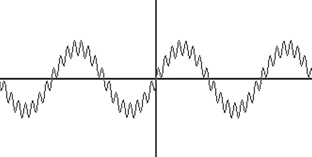
FIGURE 8-22 A two-tone test signal having a high-amplitude, low-frequency sine wave and a low-amplitude, higher-frequency sine wave. The vertical axis is amplitude, and the horizontal axis is time.
For clarity and illustration purposes, the two sine waves are locked in phase. However, normally when this test is done, in reality, the two sine waves are not locked in phase, causing a nebulous blurred look on the oscilloscope for the higher-frequency signal. The object of this test signal is to look for interaction between the two sine-wave signals that will cause other signals, intermodulation distortion products, to appear at the output of the amplifier other than harmonic distortion. However, it should be noted that the output of the amplifier will contain a combination of harmonic distortion on either or both test-tone signals plus the intermodulation distortion products. The intermodulation distortion products can be measured in two ways. One is to measure the amplitude of distortion signals centered around the high-frequency signal, and the other is to use an amplitude-modulation demodulator or envelope detector to measure the amount of amplitude modulation on the higher-frequency signal. Figure 8-23 better illustrates what is happening.

FIGURE 8-23 Test signal connected to the input signal of an amplifier (top). Output signal of the amplifier (center). High-pass filter applied to the output signal. Vertical axis is amplitude, and horizontal axis is time (bottom).
By purposely driving a one-transistor common-emitter amplifier as shown in Figure 8-24 with about 40 mV peak to peak at the input to the base of the transistor, we see that at the output (denoted by the center trace in Figure 8-23) it has distortion. The center trace shows two important characteristics. First, the low-frequency signal itself levels off on the top and does not produce a clean sine wave. Second, we can see that the higher-frequency signal’s amplitude gets smaller on the top and much larger on the bottom of the waveform. This variation in gain is consistent with what was observed in Chapter 7, which showed higher-voltage gains for higher collector currents. At the bottom of the waveform, the transistor’s collector current is at a maximum, whereas on the top of the waveform, the transistor’s collector current is at a minimum.

FIGURE 8-24 Circuit setup for IM distortion experiment.
After filtering out the low-frequency signal as shown in the center trace of Figure 8-23, the bottom trace of Figure 8-23 shows an amplitude-modulated signal with the higher-frequency signal as the carrier. Also, the envelope of the amplitude-modulated signal is not a clean sine wave but is a replica of the distorted low-frequency signal inverted in phase.
Figure 8-24 shows the amplifier used for this two-tone distortion experiment. Two signal generators, Vgen1 and Vgen1, are summed with resistors via Rgen1 and Rgen2. The input signal to the base of Q1 is about 40 mV peak to peak, as shown in the top trace of Figure 8-23. The output of the amplifier, shown as Vout, connects to C3 and R4 and has a distorted waveform, as seen in the center trace in Figure 8-23. The output of the amplifier is then connected to a high-pass filter that removes the low-frequency signal, and the HPF Out terminal passes through the higher-frequency signal, which (as seen on the bottom trace of Figure 8-23) is an amplitude-modulated higher-frequency signal. The low-frequency generator Vgen1 is at 60 Hz, and the higher-frequency signal via Vgen2 is at greater than 3 kHz.
Figure 8-24 is adapted from Figure 7-13. VR2 is adjusted to provide 2 volts DC across RE1 to set up a collector current of 200 μA. VR1 is adjusted such that the base of Q1 has a 40 mV composite waveform, as seen in the top trace of Figure 8-23.
In essence, the amplifier in Figure 8-24 acts as a multiplier of sorts by using the low-frequency signal to modulate the amplitude of the higher-frequency signal. We will find later that this circuit is commonly used as an RF mixer for radio-frequency devices.
The SMPTE (Society of Motion Picture and Television Engineers) provided an intermodulation test waveform similar to Figure 8-22 and the top trace of Figure 8-23. The low-frequency signal is at 60 Hz, and the high-frequency signal is set to 7 kHz. This is called the SMPTE IM distortion test. The amplitude mix ratio has the 60 Hz signal at 4 times larger than the 7 kHz signal. Distortion signals around the 7 kHz signal have frequencies of 7 kHz ± (n × 60 Hz), where n is a whole number greater than or equal to 1. Distortion is measured via an envelope detector such as a half-wave rectifier, an AM synchronous detector, or analysis of the distortion signals around the 7 kHz signal.
In a perfect amplifier, the high-pass filter output would show a 7 kHz signal with no variation in amplitude. So one question would be, is the amplifier in Figure 8-24 bad? For very low-level signals of less than 2 mV peak to peak, it will provide less than 1 percent distortion. For levels higher than this, the circuit distorts unacceptably for high-fidelity reproduction. However, sometimes distortion is good. We can use this circuit to enhance or change the sounds of guitar notes from an electric guitar. Distortion-making devices such as fuzz boxes deliberately distort the input signal to add more overtones to the original guitar string’s sound (see Figure 8-25).
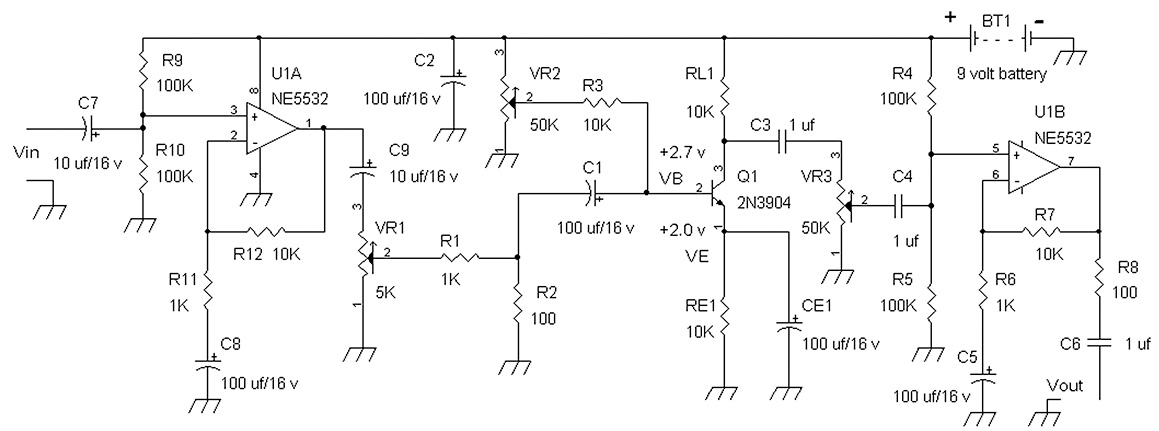
FIGURE 8-25 Experimental fuzz distortion-generator circuit.
The input signal from the electric guitar is amplified without distortion with a voltage gain of about 11 volts via U1A. The gain can be changed by increasing or decreasing the value of R12. U1A’s output is fed to VR1, which feeds into R1 the input of the distortion-generating circuit. Resistor R2 may be increased to 1 kΩ if it is desired to generate more distortion. VR1 adjusts the amount of distortion, while VR2 may be set for a particular collector current via a base bias voltage.
Sometimes it may be advantageous to set the base voltage close to 0.7 volts, near the cut-off point of the transistor, to generate even more distortion. If this is done, it may be preferable to increase the signal drive into the base of Q1 via VR1.
U1B is a gain of 11 amplifier, with VR3 setting the final distortion output level. Output capacitor C6 is meant to connect to an amplifier with 10 kΩ or more input resistance. If a low-input-resistance amplifier is connected to C6, simply increase its value to 2.2 μF or larger. A 10 μF or 33 μF capacitor can replace C6, with the positive terminal of the electrolytic capacitor connected to R8. Note that almost any dual op amp will work for U1A and U1B, such as a TL082, LM1458, RC4458, LF353, RC4560, or LM4562 op amp.
References
1. RCA Receiving Tube Manual, RC-29. New York: RCA Corporation, 1973.
2. RCA Solid-State Hobby Circuits Manual, HM-91. New York: RCA Corporation, 1970.
3. Bob Metzler, Audio Measurement Handbook. Beaverton, OR: Audio Precision, Inc., 1993.
4. Paul R. Gray and Robert G. Meyer, Analysis and Design of Analog Integrated Circuits, 3rd ed. New York: Wiley, 1993.