
CHAPTER 9
![]()
Oscillators
To generate an alternating-current (AC) signal, usually we start with an oscillator circuit. Depending on the circuit, oscillators generally provide sine-wave signals or pulsed waveforms. Other types of waveforms can be generated, such as triangle waves, which are generally derived from a square-wave generator circuit (e.g., an “on/off” circuit). This chapter will introduce the reader to some types of oscillators. There are a multitude of oscillator circuits, and some other types will be shown in subsequent chapters.
Therefore, we will explore how oscillation occurs and examine different types of oscillators used in audio and radio-frequency (RF) circuits. Also included will be relaxation oscillators, generally implemented with a resistor and a capacitor to set the oscillation frequency.
As a standalone circuit, the oscillator is a signal generator. But oscillator circuits generally are part of an overall system. As part of an overall system, the oscillator may serve as a test-tone oscillator for an audio mixer or for an RF system, the oscillator may be employed as a local oscillator for a superheterodyne radio. More important, oscillators can be varied in frequency and be part of a frequency synthesizer circuit. And in digital circuits, oscillators often are used to provide the clock signal.
It should be noted that there are no formal projects in this chapter because oscillators serve more of a support role for other projects. However, the reader is encouraged to build some of the circuits as experiments to get a feel for the various oscillators.
NOTE For this chapter and some of the succeeding ones, it is recommended that an oscilloscope be obtained to examine the waveforms from the oscillator circuits.
A Brief Overview of Oscillation Systems
Oscillation systems work on a principle of positive feedback of signals. That is, noise from the transistors or resistors acts as a “seed” to start the oscillation signal. The oscillation signal is reinforced amplitude-wise and grows to a steady-state amplitude. For this chapter, we will look into oscillators that provide both sine-wave and pulsed waveforms.
Most sine-wave oscillators use an amplifier and a phase-shift circuit. The amplifier may have a positive gain or a negative gain (e.g., inverting amplifier). See Figure 9-1.
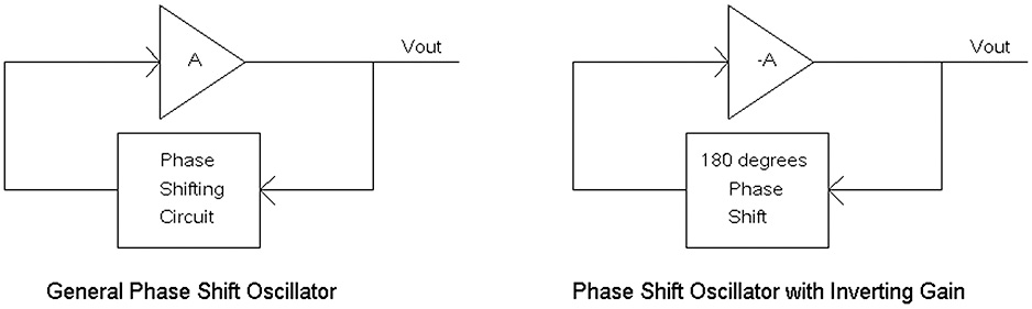
FIGURE 9-1 Oscillation systems with noninverting and inverting amplifiers.
For oscillation to occur, the system including the amplifier and phase-shift circuit has to be 0 or 360 degrees. Generally, the phase-shift circuits are implemented as high-pass, low-pass and/or band-pass filters. For an oscillation system using a noninverting amplifier, the gain of the amplifier must be large enough to overcome losses in the phase-shift circuit to provide a loop gain of at least 1. For example, if the phase-shift circuit has a loss or equivalent gain of 0.1 (1/10) at the frequency of oscillation, the amplifier’s gain A must be greater than 10 such that:
Loop gain = A × phase-shift-circuit gain > 1
In this case, let the amplifier gain A = 11 and the phase-shift-circuit gain = 0.1, which says
Loop gain = 11 × 0.1 = 1.1 > 1
The reason for having the loop gain greater than 1 is to ensure that the positive-feedback signal will reinforce itself to sustain a reliable oscillating signal. Typically, the type of phase-shift circuits that “naturally” have 0 degrees of phase shift at the resonating frequency is a band-pass filter such as a parallel or series inductor-capacitor circuit or, alternatively, some combination of a low-pass and high-pass filter.
In an oscillator using an inverting amplifier, the phase-shift circuit must provide at least 180 degrees of phase shift. A low-pass or high-pass filter using two or more capacitors or an inductor-capacitor circuit with a resistor-capacitor circuit will provide the sufficient 180 degrees of phase shift for oscillation.
Most oscillators will inherently generate a distorted sine wave such as a rectangular pulse, square wave, or triangle wave. Some RF oscillators provide sine waves via a band-pass filter that reduces harmonic distortion.
When an amplifier is configured for positive feedback with a net gain of greater than 1, the oscillation starts out as a small sine wave and grows until the sine-wave signal is clipped due to limitation of the power supply. Actually, no practical power supply can ever be great enough to escape clipping from the growing signal. This growing signal increases exponentially with passing time. Therefore, one way to control the amplitude of the oscillating signal within the range of the power-supply voltage is to apply an automatic-gain-control amplifier to lessen the gain of the positive-feedback system such that the system reaches an equilibrium for the output amplitude of the signal (see Figure 9-2).

FIGURE 9-2 An oscillator with automatic gain control to provide a distortion-free sine wave.
An amplitude-stabilized oscillator such as a Wein bridge oscillator uses a noninverting amplifier with a positive-feedback network that has 0 phase shift at the oscillation frequency. The oscillation signal starts out small in amplitude and then grows to a point where a resistor that depends on the output amplitude changes to reduce the overall gain of the noninverting amplifier.
In an automatic-gain-control (AGC) system, similar to the audio limiter amplifier mentioned in Figure 7-11, the output signal of the oscillator in Figure 9-2 is “measured” for amplitude, and there is a gain-control device (variable resistor) to adjust the gain electronically to provide a predetermined output amplitude for the oscillation signal. For example, the higher the signal increases, the more the gain is reduced. If the output amplitude is smaller than the predetermined setting, the oscillating signal will grow or increase until something close to the predetermined amplitude is achieved. One of the first ingenious devices used to maintain a steady and undistorted sine-wave signal was a simple light bulb. The light bulb, when heated, changes to an increased resistance. We saw this effect in Table 4-2 when a #222 penlight bulb was found to have a resistance of 7 Ω at 1.2 volts and 9.6 Ω at 2.4 volts.
Because the lamp is used as one of the resistors in a negative-feedback amplifier, the increased resistance causes the amplifier to reduce in gain. For example, the gain of a noninverting op amp is given as [1 + RF/RLamp], where RF is the feedback resistor from the output to the (–) input of the op amp, and RLamp is the resistance connected to the (–) input of the op amp and to ground. We can see that if the resistance of the lamp RLamp increases, the gain decreases.
Time to Sit Back and Relax for a Relaxation Oscillator (AKA Moving the Goal Posts)
Another type of oscillator known as a relaxation oscillator involves switching between two voltage levels. The gist of this system is that a resistor-capacitor circuit (e.g., a low-pass filter) receives a direct-current (DC) voltage. The capacitor charges via the resistor, and the capacitor’s voltage increases with time. Before the capacitor can charge to the final voltage, the DC voltage is switched to 0 volt to start discharging the capacitor via the resistor. When the capacitor’s voltage falls to a lower voltage, the circuit switches the DC voltage back on, and the capacitor starts charging again and its voltage increases. A cycle of charging and discharging of the capacitor is established, and thus an oscillating signal at the capacitor is provided in the form of a waveform that resembles a triangle or sawtooth waveform. Basically, as the capacitor’s voltage gets up to a certain level, it changes its mind and decides to relax and “sit down” to a lower voltage before trying to get up again (see Figure 9-3).

FIGURE 9-3 A relaxation oscillator.
A relaxation oscillator works on a principle that two voltages are determined for turning on and off the output DC voltage. That is, there are two trip voltages V1 and V2, where V1 > V2. One trip voltage is set to turn on the output, and the other trip voltage is set to turn off or ground the output signal. The 555 timer chip works on this principle as well.
For a concrete example, let’s say that V1 = 3 volts and V2 = 1 volt, which are the two different voltages available to the (+) input terminal of U1A (see Figure 9-3). The output Vout has two voltage levels, 0 volt and +V, where +V is the power-supply voltage (e.g., +5 volts). When Vout = +V, the output-dependent voltage source sends 3 volts to the (+) input of U1A, and when Vout = 0 volt, the output-dependent voltage source switches to a lower voltage and sends 1 volt to the (+) input. Thus the voltage at the (+) input is always > 0 volt.
Initially, capacitor C1 is not charged and is sitting at 0 volt coupled to the (–) input. Because the (+) input is greater than 0 volt regardless of the output voltage, the output has to be +V. Having the output at +V is good because, via R1, capacitor C1 now charges up, and the voltage across C1 increases with time. Eventually, the voltage across C1 charges to a voltage that exceeds 3 volts (V1). When this happens, all of the sudden, the output-dependent voltage source switches from V1 (3 volts) to the lower-voltage V2, which is 1 volt. With the capacitor voltage at about 3 volts into the (–) input terminal and the (+) input terminal switched or latched to 1 volt, the output of the comparator has to switch off and deliver 0 volt at the output terminal. At this point, the output at pin 1 of U1A is grounded.
Now R1 will discharge the 3 volts from the capacitor until C1’s voltage drops to slightly below 1 volt, which then causes the (+) input terminal at 1 volt to be greater in voltage than the (–) input terminal. This then results in the output going to a high level of +V, and two things happen: the voltage-dependent voltage source switches to 3 volts, and C1 starts charging up again from 1 volt towards 3 volts via R1 connected to the output of U1A. This cycle of charging and discharging C1 between 1 volt and 3 volts repeats itself and forms an oscillating waveform similar to a sawtooth across C1. The manner in which the output-dependent voltage source provides its signal to the (+) input terminal is akin to “moving the goal posts” as to what the threshold or switching voltages are. Thus the voltage across C1 is being compared with a time-varying voltage, which is responsible for making the circuit an oscillator. We will return to relaxation oscillators in more detail later, but now let’s look at some other oscillator circuits.
Phase-Shift Oscillators
One type of phase-shift oscillator includes an inverting-gain amplifier with either multiple high-pass or low-pass filters that use a resistor and capacitor for each phase-shift section. Each phase-shift section of a high-pass filter provides up to +90 degrees of leading phase shift, and each section of a low-pass filter provides up to –90 degrees of lagging phase shift. Note that when we talk about phase shift, we are applying the phase shift to a sinusoidal signal.
Although, in theory, two sections of a resistor-capacitor filter can provide up to 180 degrees of phase shift, the amplitude response at the 180-degree phase-shift frequency is generally so low that an extremely high-gain amplifier is needed. Also, the lagging phase shift inherent in the amplifier may cancel some of the leading phase shift in a phase-shift oscillator circuit using two high-pass filter sections. This will cause the total phase shift to be less than +180 degrees and prevents oscillation.
To allow for reliable oscillation, usually three or more sections of phase shift are used. The most common phase-shift oscillators involve three sections of resistor-capacitor (RC) high-pass or low-pass filters (see Figure 9-4).
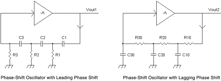
FIGURE 9-4 Phase oscillator system using three high-pass and three low-pass filters to form leading and lagging phase shifts.
By using a series of high-pass filters via C1 R1, C2 R2, and C3 R3, a phase shift of up to 3 × +90 degrees = +270 degrees is possible from the output of the inverting amplifier with gain –A connected to the C1 input, which is connected to R3. The positive or leading phase shifts will occur at frequencies below the cut-off frequency of the high-pass filter. For example, if we take a one section filter comprised of C1 and R1 and design it for a high-pass filter at 1 kHz, the filter will pass frequencies above 1 kHz (e.g., 2 kHz) but attenuate signals whose frequencies are below 1 kHz (e.g., 500 Hz). These attenuated signals below 1 kHz will exhibit a positive phase shift. With the three-section high-pass filtering that provides a leading phase shift from the output of the amplifier to the input, there will exist an oscillation frequency below 1 kHz such that a phase shift of +180 degrees is provided. For simplicity, some designs have C1 = C2 = C3 and R1 = R2 = R3. A variable-frequency oscillator can be made with a three-ganged variable resistor for R1 to R3, but each section should have a series resistor so that the R1 to R3 cannot go to 0 Ω. For example, a 100 kΩ three-section variable resistor with a 1 kΩ series resistor for each of the three sections provides a frequency adjustment of about 100:1.
Also shown in Figure 9-4 is a phase-shift oscillator with phase lag (negative phase shift) using three RC low-pass filters, R10 C10, R20 C20, and R30 C30, to provide a maximum phase shift of 3 × –90 degrees = –270 degrees. If we again set the low-pass filter to a cut-off frequency of 1 kHz, signals with frequencies below 1 kHz (e.g., 500 Hz) will pass relatively unattenuated from R10 to C30, but signals that have frequencies above 1 kHz (e.g., 2 kHz) will be attenuated in amplitude and have a phase lag. The oscillation frequency then has to be above 1 kHz in this example to provide the necessary –180 degrees of phase shift. For a practical example of a phase-shift oscillator, see Figure 9-5.
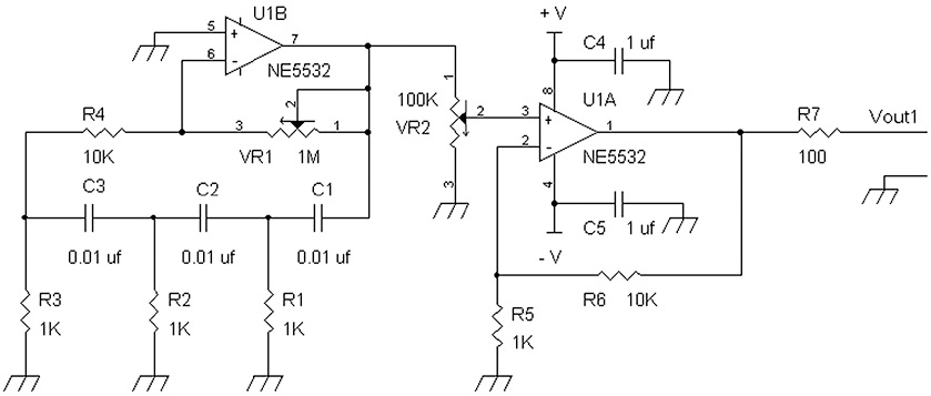
FIGURE 9-5 A phase-shift oscillator using an op amp and three-section high-pass filter.
This oscillator uses equal values for C1–C3 at 0.01 μF and 1 kΩ resistors for R1–R3, and the power supply can be anywhere from ±9 volts to ±15 volts. An inverting gain of about 43 is set by VR1 at 430 kΩ. Recall that the gain in this circuit is about –VR1/R4 = –430 kΩ/10 kΩ = 43. VR1 may be replaced with a 510 kΩ resistor with 5 percent tolerance to ensure oscillation.
The oscillation frequency was measured at about 6 kHz. Thus, at 6 kHz, the high-pass filter provides a phase shift of about +180 degrees. The approximate cut-off frequency is based on the formula for cut-off frequency of a one-section high-pass filter being 1/(2πR1C1) and is about 16 kHz, which means that the measured oscillation frequency is less than half the calculated cut-off frequency.
To change the oscillation frequency, one can replace all the capacitors C1–C3. Based on the frequency of oscillation measured at 6 kHz for 0.01 μF, the approximate frequency is then:
fosc_HPF = 6 kHz × 0.01 μF/C1
For example, if C1 = 0.1 μF = C2 = C3, then:
fosc_HPF = 6 kHz × 0.01 μF/0.1 μF = 6 kHz × 1/10 = 600 Hz
One can also vary the oscillation frequency by changing resistors R1, R2, and R3. For example, if their values are increased, the oscillation frequency should be lowered.
Note that, in practice, even after adjusting VR1 for the lowest sine-wave distortion, the output waveform is clipped or slightly distorted [approximately 3 percent total harmonic distortion (THD)]. Because there is no automatic gain control (AGC) mechanism in this oscillator, the sine-wave output signal has to go into some type of limiting that distorts the waveform. The output of the oscillator at U1B is connected to level control VR2, which is connected to a gain of 11 amplifier U1A.
Now let’s take a look at a phase-shift oscillator using low-pass filtering (see Figure 9-6).

FIGURE 9-6 A phase-shift oscillator using a multiple-section low-pass filter.
In Figure 9-6, we turn the high-pass filter circuit from Figure 9-5 into a three-section low-pass filter comprised of R10 C10, R20 C20, and R30 C30. Power-supply voltages may be from ±9 volts to ±15 volts. The gain was set to about –23 with VR10 set to about 220 kΩ for a gain of –(VR10/R40) = –(220 kΩ/10 kΩ) = –23. Note a 220 kΩ to 270 kΩ resistor may be substituted for VR10.
Again, the cut-off frequency based on R10 and C10 is calculated as 1/(2πR10C10) = 16 kHz. However, we will expect the oscillation frequency to be maybe twice the cut-off frequency. This guess is based on the high-pass-filter phase-shift oscillation frequency being less than half the calculated frequency. The oscillation frequency was measured at about 31 kHz, which is about twice the calculated cut-off frequency. Thus the low-pass filter network comprised of R10 C10, R20 C20, and R30 C30 provided a phase shift of about –180 degrees at 31 kHz.
We can then figure out how to scale capacitors C10, C20, and C30 to provide a new oscillation frequency. Based on what was measured, the frequency of oscillation is given by:
fosc_LPF = 31 kHz × 0.01 μF/C10
For example, if C10 = 0.1 μF = C20 = C30, then:
fosc_LPF = 31 kHz × 0.01 μF/0.1 μF = 31 kHz × 1/10 = 3.1 kHz
Similarly, we can change the resistance values to change the oscillation frequency. By increasing the resistor values for R10, R20, and R30, we would expect a lowering of the oscillation frequency.
We know that the output of U10B will deliver a clipped sine wave, so it would be advantageous to take the oscillator’s signal after the low-pass filter section that reduces harmonic distortion signals. Thus we see that VR20 is connected to C30 instead of pin 7 of U10B. The output amplifier U10A provides a clean, nonclipped sine wave (<2 percent THD)—well, at least it’s cleaner than the clipped waveform from Figure 9-5, U1A’s output.
NOTE For the phase-shift oscillators in Figures 9-5 and 9-6, the choice of the op amp is important concerning the highest-frequency oscillation. An NE5532 was chosen because it is about 10 times faster than an LM1458 or LM741. The NE5532 with a 10 MHz gain bandwidth product (GBWP) allows it to oscillate with good performance for typical audio test frequencies up to 20 kHz. Also, an LM4562 with a 55 MHz GBWP should provide about 5 times higher in oscillation frequency than the NE5532.
Now we turn to using a nonlinear resistor such as a light bulb to provide automatic gain control of an oscillator circuit so that the output sine-wave signal, without filtering, is not clipped.
Wein Bridge Oscillator with Automatic Gain Control to Provide Non-Clipped Sine Waves
A basic sine-wave oscillator includes a non-inverting-gain amplifier where one of the feedback resistors changes value such that the gain is lowered when the output voltage is increased (see Figure 9-7).
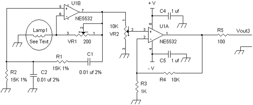
FIGURE 9-7 A Wein oscillator circuit using a low-current lamp to regulate the output amplitude.
The oscillator section is implemented by U1B, and its output signal is fed to VR2, a level control for output amplifier U1A. The output of U1A then provides a sine-wave signal by adjusting VR1 for an output of about 2 volts peak to peak at pin 1 of U1A. Lamp1 is rated at 6 volts, 25 mA and has RadioShack part number 272-1140. The power-supply voltages can be ± 9 volts to ±15 volts.
This oscillator includes a non-inverting-gain amplifier, U1B, whose gain = [1+ (VR1/RLamp1)]. A positive-feedback network is formed by C1, R1, C2, and R2. If we look at this network intuitively, a very crude approximation of it would be that C2 forms a low-pass filter with R1 and R2 forms a high-pass filter with C1.
If R1 = R2 and C1 = C2, then we will find after a bunch of messy calculations that this network will provide 0 degrees of phase shift at a resonant frequency:
fr = 1/(2πR1C1)
Given for this example that R1 = 10 kΩ and C1 = 0.01 μF, thus:
fr = 1/(2π × 10 kΩ × 0.01 μF) ≈ 1.6 kHz
In terms of providing a variable-frequency Wein oscillator, there is a way to implement this. One can replace R1 and R2 with a twin-gang variable resistor such as a stereo potentiometer. To avoid having 0 Ω for R1 and R2, a small-valued series resistor such as a 1 kΩ resistor can be connected in series with each of the two potentiometers.
And at the resonant frequency, there is a loss in signal of 1/3 from the output of U1B to its (+) input terminal. For example, if there are 2 volts of AC signal at the output of U1B at pin 7, the AC signal at the (+) input of U1B pin 5 has an amplitude of (2 volts)/3 = 0.667 volt.
Because we require a loop gain of greater than 1 to maintain a reliable oscillation, the non-inverting-gain amplifier, whose gain is [1+ (VR1/RLamp1)] must be greater than 3. That is:
(1/3)[1 + (VR1/RLamp1)] > 1
For this circuit, a 6 volt, 25 mA lamp bought at RadioShack (part number 272-1140) was used along with a ±9 volt battery power supply. Note that up to a ±15 volt supply can be used. VR1 was adjusted to an output level of about 1.94 volts peak to peak at pin 7 of U1B. The total harmonic distortion (THD) was < 0.03 percent (< –70 dB). Another lamp that can be used is a 12 volt, 25 mA bulb from RadioShack (part number 272-1141).
Although many lamps that are rated at 25 mA or less can be used, bulbs with higher current ratings may cause the 5532 op amp’s output stage to go into current limiting. When an amplifier’s output stage is driven into current limiting, this results in clipping or distorted signals. To boost the current capability of the op amp, two transistors, Q1 and Q2, and a resistor, R6, are added (see Figure 9-8).

FIGURE 9-8 A Wein oscillator with a current-boosting output stage.
NPN transistor Q1 provides increase current to be sourced in the positive direction, while PNP transistor Q2 allows for more current to be sunk in the negative direction. Resistor R6 passes the signal from the op amp’s pin 7 for small amounts of current up to about 7 mA into VR1 and Lamp1. If Lamp1 draws more than 7 mA in positive and negative directions, resistor R6 at 100 Ω develops 0.7 volt across the base-emitter junctions of Q1 and Q2 to turn them on and dump extra current into Lamp1. Note that 7 mA × 100 Ω = 0.7 volt.
Transistors Q1 and Q2 provide the extra current via the +V and –V power supplies connected to their collector terminals. The NE5532 has about 30 mA of output current before its current-limiting circuit is enabled. This means that there are at least 30 mA – 7 mA = 23 mA available to drive the bases of Q1 and Q2. The boosted current capability is then about β(23 mA), where β is the current gain of the transistors. Typically, we can assume that β =10 at “high” currents for the 2N3904 and 2N3906 transistors. So we now have about 230 mA of output current available instead of 30 mA. With this extra current capability, we can now use higher-current light bulbs that are more common.
Output voltages at VOSC, pin 1 of VR2, are in peak-to-peak (p-p) voltages as adjusted by VR1. The output voltages may be adjusted to higher or lower sine-wave amplitudes. The tests were made with ±9 volts for the power supply, and other supply voltages may be used, such as ±12 volts or ±15 volts. See Table 9-1 and note that p-p voltage denotes peak to peak voltage.
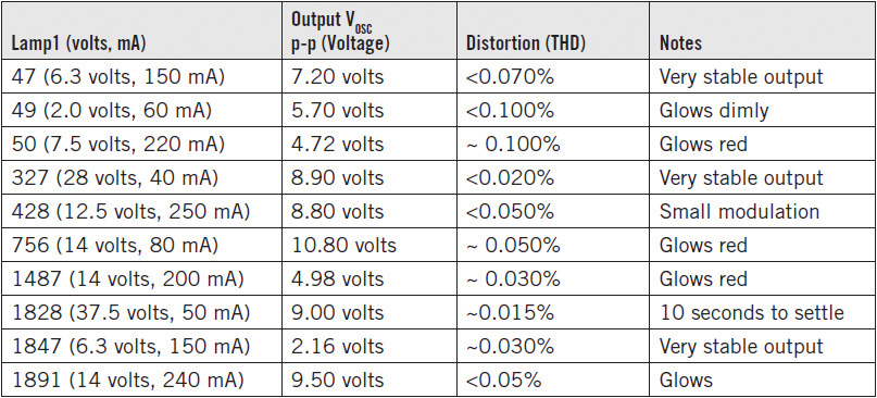
TABLE 9-1 Results of Various Lamps for the Wein Oscillator Circuit in Figure 9-8
A Universal Wein Oscillator Circuit
Using 2N3904 and 2N3906 transistors is fine for driving up to about 100 mA, but beyond the 200 mA of current that they are rated for, the current gain of the transistors falls off sharply to a much lower current gain. A fix to increase the output-current capability is to simply use very high-power transistors such as the TIP41 (NPN) and the TIP32 (PNP). These power transistors have a pin-out of BCE instead of the EBC used in the 2N3904/2N3906 transistors (Figure 9-9).
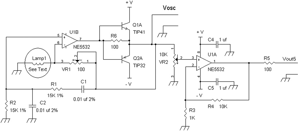
FIGURE 9-9 A universal Wein oscillator circuit with power transistors Q1A and Q2A.
The TIP32 transistor is a 3 amp device, whereas the TIP41 handles 6 amps of collector current. In terms of current gain b, with 23 mA into the base, the minimum β is about 40 to deliver about 800 mA of current into the Lamp1. Other power transistors can be used, such as the MJE3055 or TIP3055 (NPN) and the MJE2955 or TIP2955 (PNP). See the results in Table 9-2 with higher-current lamps where the supply voltages are ±9 volts to the oscillator.
TABLE 9-2 Universal Wein Oscillator Circuit in Figure 9-9 with Higher-Current PR-2 and PR-4 Flashlight and #112 and #222 Penlight Bulbs
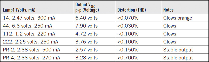
In terms of the notes for Tables 9-1 and 9-2, all bulbs produced stable amplitude waveforms except the #428 lamp. The #428 bulb had some small signs of “breathing,” or very low-frequency amplitude modulation of the sine wave.
Relaxation Oscillators
These types of oscillators are often used for voltage-controlled oscillators at low frequencies and are also commonly the heart of analog function generators. Although the oscillation frequencies are generally below a few MHz (megahertz), very high-frequency versions can oscillate in the tens of MHz (megahertz). Let’s examine them now. Figure 9-10 shows a very low-frequency oscillator.

FIGURE 9-10 A relaxation oscillator circuit using an LM358 op amp (left) and a circuit using a Thevenin equivalent with R2||R3 and +4.5v (right).
In this example, U1A is an op amp but functions as a comparator. In Figure 9-10 (left) we have an RC low-pass filter R1 and C1 connected from the output terminal of U1A, pin 1. The voltage across C1 is connected to the (–) input terminal of the op amp. Also connected to pin 1 is a logic inverter circuit Q1 and R4. The output of the op amp will be a rectangular pulse waveform, and thus relaxation oscillators are not sine-wave generators like the previous circuits. The output of inverter Q1 via its drain terminal is connected to the gate of Q2. Note that Q1 and Q2 may be 2N7000, VN2222, or VN10K. As mentioned previously, a relaxation oscillator includes an output-dependent voltage source that provides two different voltages to the (+) terminal of the LM358.
In Figure 9-10 (right), the voltage-divider circuit R2 and R3 with a 9 volt source is simplified with a Thevenin equivalent circuit, and the voltage-divider circuit is expressed as a 4.5 volt source driving a Thevenin resistance of R2||R3 = 5 kΩ.
NOTE Any two-resistor voltage-divider circuit can be expressed by a voltage source that represents the divided voltage and a series resistor whose value is the parallel resistances of the two resistors. This new circuit is commonly called a Thevenin equivalent circuit.
We now turn to Figure 9-11, which shows the two states of Q2, which are “off,” an open circuit, and “on,” a short to ground. Pertaining to R5, Q2 then acts as an open circuit or as a switch to ground.
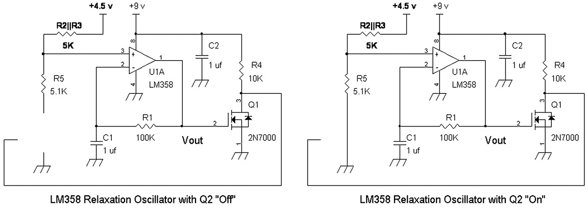
FIGURE 9-11 Relaxation oscillator showing the two states of Q2.
Initially, capacitor C1 is sitting at 0 volts. So, regardless of whether Q2 is on or off, the voltage at the (+) terminal of U1A will be > 0 volt. We know this because when Q2 is off, the voltage at the (+) terminal is 4.5 volts, and if Q2 is on, the voltage would be roughly 2.5 volts via a voltage-divider circuit from the 4.5 volt feeding R2||R3 and R5. Because R2||R3 is about the same resistance as R5, we get roughly half the 4.5 volts into the (+) terminal or pin 3 of U1A.
With the voltage at the (+) terminal greater than the voltage initially at the (–) terminal of the comparator, the output has to be a logic high voltage, which is typically close to 9 volts. The output voltage then charges up C1 via R1. The logic high voltage from the output Vout is also connected to Q1’s gate. This produces a logic low into the gate of Q2 (see Figure 9-10), which confirms that Q2 is off, as seen on the left side of Figure 9-11, and that there is 4.5 volts connected to the (+) input terminal of U1A.
The logic high voltage from pin 1 of U1A will then continue to charge up C1 via R1 until C1’s voltage into the (–) input terminal exceeds 4.5 volts. When this happens, the output of U1A goes low and sends 0 volt to the gate of inverter Q1, which then outputs a logic high voltage to the drain of Q1 via R4. Because the gate of Q2 is connected to the drain of Q1, Q2 then turns on and shorts or connects R5 to ground (see Figure 9-11, right).
Once R5 is connected to ground as shown, a voltage divider is set up by R2||R3 and R5, and the voltage to the (+) input terminal is changed from 4.5 volts to roughly half that, or 2.25 volts, to the (+) input terminal of U1A. Because the C1’s voltage is around 4.5 volts at the (–) input terminal, which is greater than 2.25 volts at the (+) input terminal, Vout goes to 0 or ground, which starts C1 to discharge. Eventually, C1’s voltage will decrease to just below 2.25 volts into the (–) input terminal with 2.25 volts still at the (+) input terminal. Once this happens, Vout goes back to a logic high state and starts charging up C1, while Q2 reverts to an open-circuit state. With Q2 at an open-circuit state, the voltage into the (+) input terminal changes from 2.25 volts back to 4.5 volts.
The cycle will just repeat itself, and a sawtooth waveform across C1 will be formed, where the positive and negative peaks of the sawtooth are at 4.5 volts and 2.25 volts. The output, Vout, will provide a periodic pulsed waveform with a frequency of about 7.9 Hz given that C1 = 1 μF (film capacitor with 5 percent or lower tolerance) and R1 = 100 kΩ.
NOTE Normally, film capacitors with 5 percent tolerance or better are used in RC oscillators. Even for large values at 1 μF or more, it is better to use film (e.g., polyester, Mylar, polycarbonate, etc.) than to use electrolytic capacitors that typically have tolerances of +80 percent and –20 percent. If the frequency or pulse width does not need to be accurate, electrolytic capacitors can be used. But, as a reminder, note the polarity. With positive pulses at the output, usually the negative side of the electrolytic capacitor is grounded.
Now that we have looked at one example of a relaxation oscillator, let’s look at another. Figure 9-12 uses an LM393 comparator to allow for higher oscillation frequencies over the LM358 op amp version. Again, Q1 and Q2 may be 2N7000, VN2222, or VN10K.
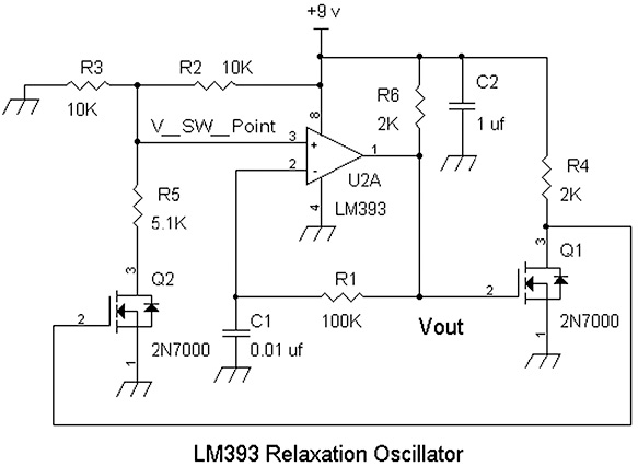
FIGURE 9-12 An LM393 relaxation oscillator.
We basically have the same circuit as Figure 9-10 (left) but with a “real” comparator to replace the slow-moving LM358. Many comparators have an open collector output stage, which requires a pull-up resistor (R6). The pull-up resistor’s value at 2 kΩ is chosen as a compromise of speed and power dissipation. Too low of a value (e.g., 50 Ω to 500 Ω) in the pull-up resistor (R6) can damage the output transistor, whereas too high a value for R6 will cause a slowness in response, even though the power dissipation into the output stage of the LM393 will be lower. C1 is about 100 times lower in this schematic to show that this circuit can oscillate at a higher frequency than the LM358 version. The switch-point voltages are still the same here at 4.5 volts and approximately 2.25 volts.
Another way to design a relaxation oscillator is to include a hysteresis resistor (R7) to generate the two switch-point voltages into the (+) input terminal of the comparator (see Figure 9-13).
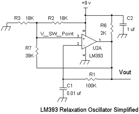
FIGURE 9-13 A simplified relaxation oscillator circuit that does not require Q1 and Q2.
In this oscillator, the current through R7 is different when Vout is a logic high and a logic low. We still have the same RC circuit R1 and C1 to charge and discharge the capacitor for providing a voltage at the (–) input terminal of the comparator. When the output is logic high at +9 volts, we have about 93 uA flowing into the voltage-divider circuit R2 and R3, which adds 0.843 volt to the 4.5 volts to provide 5.34 volts (4.5 volts + 0.834 volt) to the (+) input. When the output is low, we subtract 0.834 volt from the 4.5 volts = 3.65 volts because we have 93 μA flowing out of the voltage-divider circuit. Thus, in Figure 9-13, there is a sawtooth waveform across C1 that is bounded by 5.34 volts and 3.65 volts. To vary the oscillation frequency, R1 can be replaced with a potentiometer (e.g., 500 kΩ) or C1 can be changed to another value.
So far, we have seen a few different types of relaxation oscillators. One should note that these relaxation oscillators will change oscillation frequency if the power supply voltage varies. Thus it is recommended that these circuits (e.g., Figures 9-10 through 9-13) be connected to a regulated power supply (e.g., +9 volts or +12 volts).
Just for Fun, Build a 555 Timer with a Dual Comparator, FET, and a Flip-Flop
The following is more of an exercise to lift the block diagram of the 555 timer and implement it with other parts. We will show how to make an astable or free-running oscillator. This circuit is more for the fun of building it. Figure 9-14 shows the block diagram.

FIGURE 9-14 A 555 timer block diagram.
The 555 timer circuit uses two comparators instead of one, as seen in previous circuits. To operate as an oscillator, the top comparator (U1A) is fed two-thirds of the supply voltage +V at its (–) input terminal, whereas the bottom comparator (U1B) is fed a one-third supply-voltage reference.
Initially, capacitor C is at 0 volt, and the output of U1B is logic high because there is 1/3 the supply voltage at the (+) terminal of U1B. However, the output of top comparator U1A is logic low because the +(2/3)V voltage at the (–) input terminal is greater than the initial 0 volt across the capacitor C, which is connected to the (+) terminal of U1A. So we are safe in that we do not want the RS flip-flop circuit to have a logic high at both R and S inputs. With U1B outputting a logic high voltage to the Set or S input of RS flip-flop U2, the Qout output is low and Q1 is off. Qout is the inverted logic output of Qout. The Qout output of the flip-flop will stay low even if the voltage drops to a logic low into the S input.
The flip-flop has a memory, and Qout can only change states when there is a low- to high-level signal at the R input. Therefore, via V+ connected to RA and RB in series, capacitor C is charging, and over time, the voltage increases such that eventually the capacitor voltage slightly exceeds (2/3) of the supply voltage, and the top comparator outputs a high logic level to the flip-flop circuit that causes Qout to go to a high logic level and turn on Q1 to start discharging C via RB. When the voltage of C drops slightly below (1/3)+V, the bottom comparator outputs a logic high voltage to the S input of U2, and Q1 shuts off and becomes an open circuit to allow C to start a charging process again via +V, RA, and RB. As a result of the flip-flop latching on and off as the capacitor voltage charges and discharges between two-thirds and one-third of the power-supply voltage, an oscillation is provided. The output voltage is taken from the Qout terminal that provides a periodic pulsed waveform. For a circuit implementation, see Figure 9-15.

FIGURE 9-15 An equivalent 555 oscillator circuit.
For this circuit, the dual comparators are in a LM393, and the flip-flop circuit is implemented by cross-connected NOR gates U2C and U2D. U2 can be of a 74HC02, 74AHC02, or 74AC02 NOR gate. The supply is regulated via the 7805T chip to provide 5 volts to U1 and U2. Q1 may be a 2N7000, VN2222, or VN10K MOSFET.
A MOSFET (Q1) is used for the transistor switch, but it is possible to replace Q1 with a 2N3904 transistor, provided that there is a 1 kΩ resistor in series with the base so that pin 13 of U2 is driving the base via the 1 kΩ resistor. Otherwise, the output at pin 13 of U2D will be clamped to less than 1 volt, and the circuit will not work. Note the two-thirds and one-third supply-voltage references at pin 2 U1A and pin 5 U1B are implemented via three equal-valued resistors R1, R2, and R3.
In all the relaxation oscillator examples, there are two voltages that activate the comparator to form a boundary of voltages for the sawtooth waveform across the timing capacitor. The voltage difference between the two (threshold) voltages is also called the hysteresis voltage. For example, in the LM358 oscillator, the two voltages are 4.5 volts and 2.25 volts, which result in a hysteresis voltage of 4.5 volts – 2.25 volts = 2.25 volts.
To Wrap Up Relaxation Oscillators, Just Use a 74HC14 or 74AC14 Chip
After all the relaxation oscillators presented, probably the easiest circuit to use is an inverter logic gate that has a hysteresis input stage. The hysteresis input stage has two different voltages for turning on and off the gate and is equivalent to a comparator with a voltage-dependent voltage source that changes the voltage thresholds of turning on and off. For a 74HC14 gate, for example, with a 4.5 volt supply, the positive-going threshold voltage is typically 2.7 volts, and the negative-going threshold voltage is 1.8 volts, which leads to a hysteresis voltage of:
2.7 volts –1.8 volts = 0.9 volt
See Figure 9-16. The 74HC14 oscillator is capable of generating signals whose frequencies are in the MHz. If higher frequencies are desired, a 74AC14 gate can be used instead to provide an oscillation frequency well into the tens of MHz. Also, using an HC or AC 7400 series logic device such as a 74HC14 or 74AC14 produces a waveform that is nearly a 50 percent duty-cycle squarewave. Note that these chips have a maximum voltage rating of about 6 volts and should be connected to a regulated power supply to ensure safe operation and for frequency stability of the oscillation signal.
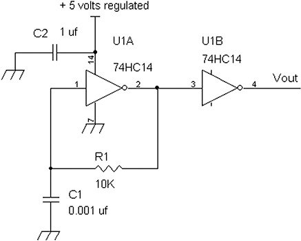
FIGURE 9-16 A minimum parts relaxation oscillator that is capable of high-frequency generation.
Radio-Frequency (RF) Oscillators
For both radio transmitters and receivers, oscillators play an important role. They provide signals that are stable in frequency for transmitting and variable frequencies for tuning across the band. Although these days many of the “analog” oscillator signals are replaced with frequency synthesizer chips such as the Analog Devices AD9851, RF oscillators are still being used in low-power applications and for many do-it-yourself (DIY) hobbyist radio circuits. We will touch on some basic RF oscillator circuits here, and other types will be addressed in Chapters 10 and 11.
We will start with a Colpitts oscillator, a zero-degrees phase-shift oscillator, which is often used in fixed- and variable-frequency oscillators. Let’s first take a look at a block diagram of a basic zero-phase-shift oscillator (see Figure 9-17).
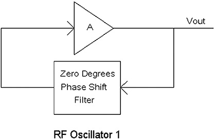
FIGURE 9-17 An RF oscillator having a zero-phase-shift positive-feedback network (e.g., parallel inductor-capacitor bandpass filter).
Many RF oscillators use a parallel LC (inductor-capacitor) bandpass filter, where at the resonant frequency, the phase shift is 0 degrees and at below the resonant frequency there is a positive phase shift and at above the resonant frequency, there is a negative phase shift. Maximum output of the bandpass filter is at the resonant frequency. In Figure 9-17, an amplifier with noninverting gain is fed to the zero-degrees phase-shift filter. Should the amplifier have some phase lag due to fall-off in high-frequency response, an extra phase lag will be incurred in this oscillating system. So, to ensure that oscillation occurs, the oscillator will “magically” move the frequency of oscillation slightly lower than the resonant frequency because the phase-shift filter has a phase lead at frequencies below the resonant frequency. This phase lead will then cancel the phase lag from the amplifier to ensure that there is always a 0-degree phase shift in the system. And this explains why an oscillator with slower transistors may oscillate at a lower frequency than one with higher-frequency transistors.
Now let’s look at the example circuit shown in Figure 9-18. A Colpitts oscillator generally uses a capacitive voltage divider to provide a 0-degree phase signal into the input of the amplifier. In this case, the emitter serves as the input terminal. Normally, we would think of the base of a transistor as the input terminal or point. However, in this case, the base of Q1 is grounded AC-wise via C4, which then makes Q1 a grounded base or common-base amplifier. The use of C1 and C2 is to form an impedance-matching network that steps down the signal across L1 and provides a low-impedance drive to the emitter. R3 generally sets the collector current sufficiently high to provide gain in the system to sustain a reliable oscillation. One can experiment with changing the values of R3.
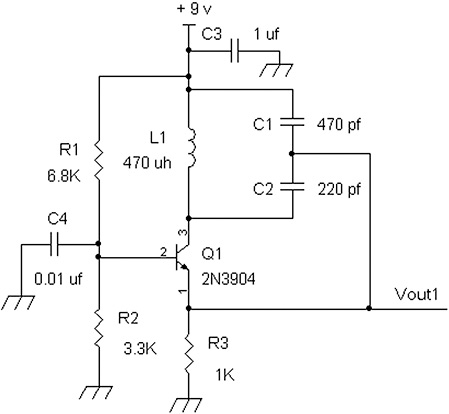
FIGURE 9-18 A Colpitts oscillator with a capacitive voltage divider formed by C1 and C2.
NOTE Math Stuff (Not Really Required Reading, But if You Are Curious): In common-base amplifiers, the input resistance into the emitter is approximately 1/gm, where gm = ICQ/0.026 volt and ICQ is the collector current. In this example, via voltage divider R1 and R2 and a 9 volt supply, the base voltage is about 3 volts, and with a 0.7 volt VBE, there is about 2.3 volts DC at the emitter. The emitter current is then 2.3 volts/R3 = 2.3 volts/1 kΩ = 2.3 mA ≈ ICQ because emitter and collector currents are essentially the same in this case. The input resistance into the emitter is then about 11 Ω = 0.026 volt/2.3 mA.
The oscillation frequency is given by ![]() where L1 is the 220 μH coil in Figure 9-18, and C = C1C2/(C1 + C2), the series capacitance of C1 and C2. For this circuit:
where L1 is the 220 μH coil in Figure 9-18, and C = C1C2/(C1 + C2), the series capacitance of C1 and C2. For this circuit:
C = (470 pF × 220 pF)/(470 pF + 220 pF) = 150 pF
Thus:
![]()
The output amplitude can be controlled by changing R3 and/or by adding a resistor in parallel with L1 (e.g., 10 kΩ to 100 kΩ). Because of the bandpass filtering characteristics of L1, C1, and C2, the output waveform is sinusoidal, even though the collector current resembles a pulsed waveform.
Let’s now move onto another oscillator that is used in AM and shortwave radios. Figure 9-19 shows the block diagram.

FIGURE 9-19 An oscillator with an inverting amplifier and a 180-degree phase shifter.
Typically, oscillators of this kind use a common-emitter or common-source configuration. The 180-degree phase shift is actually provided by a transformer. Oscillator coils made for solid-state circuits routinely have primary and secondary windings. The transformer itself includes inductance to resonate with a capacitor (Figure 9-20).
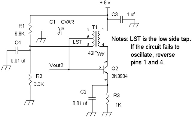
FIGURE 9-20 A typical AM or shortwave radio oscillator circuit using a transformer and common-emitter amplifier.
Transformer T1 allows a phase inversion to occur by the connections of the secondary winding, denoted as pins 1 and 4. Q2 serves as a common-emitter amplifier because C2 is low impedance at the oscillating frequency. R3 determines the amplitude of the sine-wave output, and its value can be in the range of 10 kΩ to 1 kΩ.
In this circuit, the variable capacitor has a range of about 10 pF to 60 pF. This variable capacitor with an oscillator coil (~440 μH), T1 a 42IF300 or 42IF110 (Xicon) or equivalent, will provide a frequency range of about 990 kHz to about 2.1 MHz, the frequency range of an AM radio’s local oscillator. On the primary side of T1, pins 6 and 8 are the low-side tap of the primary winding. By low-side tap, we mean that the primary winding is not tapped symmetrically and that there is a lower-resistance winding between pins 6 and 8 than at the higher-side tap at pins 5 and 6. The low-side tap is required to load into the base of Q1, which has a medium input resistance (e.g., 300 to 3 kΩ).
Sometimes building one of these circuits with the transformer is tricky, and the circuit may not oscillate. If this happens, confirm the low-side tap or reverse pins 5 and 8 to see if the circuit then oscillates. Also try reversing pins 1 and 4. Pins 5 and 8 of T1 (~440 μH) form the inductance for variable-capacitor C1.
The Colpitts oscillator in Figure 9-18 and the one in Figure 9-20 are probably the most common types of oscillator circuits. But there are other types. Figure 9-21 shows a block diagram of a different type of oscillator.

FIGURE 9-21 An oscillator with noninverting gain of approximately +1, where the phase-shift network is divided into two stages, a phase-lag and a phase-lead circuit.
The type of oscillator seen in Figure 9-21 uses an emitter-follower or source-follower amplifier. Oscillation occurs when there is a phase-shift lag in one circuit that is coupled to another circuit that provides a leading-phase shift. The net phase shift cancels out from output to input of the amplifier. Because the amplifier itself has a gain approximately +1, we need to provide some type of voltage gain. The leading phase-shift circuit, a high-pass filter, has a peaky response that provides voltage gain at the resonant or oscillation frequency.
In some instances, this type of oscillator sometimes represents an amplifier going into a very high-frequency parasitic oscillation. The output of the amplifier is connected to a capacitive load, and the internal capacitance of the transistor between the base and emitter (or gate and source) is connected to wire or trace to form a small-valued inductor that is eventually AC grounded. The result is a parasitic oscillation.
In general, though, this type of configuration does provide reliable oscillation when used with inductors (see Figure 9-22).

FIGURE 9-22 An emitter-follower oscillator.
Here is a circuit that oscillates at about 700 kHz. Q3 is an emitter follower that is biased at about 100 μA such that its output resistance at the emitter approximately 1/gm ≈ 260 Ω, where gm = ICQ/0.026 volt and ICQ is the collector current. The output resistance at 260 Ω and CE = 1,800 pF forms a low-pass filter at 1/(2π 260 Ω 1,800 pF) = 340 kHz. A low-pass filter at 340 kHz provides a lagging phase shift at the frequency of oscillation, which is approximately ![]()
To determine a more exact oscillation frequency, CE must be part of the equation because it is in series with C1. CE and C1 in series is (220 pF × 1,800 pF)/(220 pF + 1800 pF) = 196 pF, which leads to an oscillation frequency of:
![]()
Again, the lagging circuit is formed by the output resistance of Q3 and CE. Capacitor C1 is then coupled to L1 to form a high-pass filter with a positive or leading phase. The net phase shift from the emitter of Q3 to its base is then 0 degree because the lagging and leading phase shifts cancel out.
But the main question is, if an emitter follower has a gain of less than 1, where does the extra gain come from? If we look carefully, L1 is AC grounded via C2, and thus Q3’s emitter drives a series-resonant circuit C1 and L1. At resonance, the impedance of a series LC circuit is low. Thus there are huge amounts of current flowing through C1 and L1 at the resonant frequency, as provided via the emitter of Q3. The large AC current flowing through L1 steps up the voltage from the emitter of Q3. By stepping up the voltage from the emitter of Q3 to the base, we get a net gain of more than 1 in the system. So it turns out that C1 and L1 behave like a step-up transformer for signals at the resonant frequency.
Voltage reference diode LED1 provides a “stable” 1.8 volts DC into the base of Q3 via L1. And the emitter current is then 1.8 volts – VBE ≈ 1.2 volts across RE, given that the VBE turn-on voltage of Q3 is approximately 0.6 volt. The collector current ICQ ≈ 1.2 volts/RE = 1.2 volts/12 kΩ = 100 μA.
Finally, we turn our attention back to a common-emitter amplifier oscillator. This type of oscillator is commonly used also for the Pierce crystal oscillator, where the inductor is replaced by a crystal and the capacitors at the collector and base are adjusted to cause the crystal to allow for oscillation. Let’s take a look at the block diagram first (see Figure 9-23).
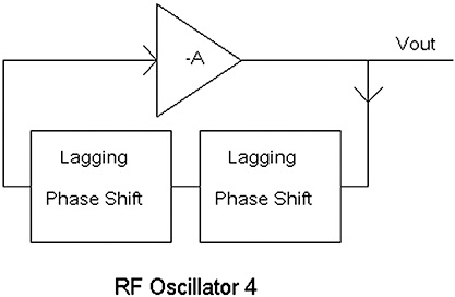
FIGURE 9-23 A two-stage phase-lagging network to provide oscillation.
Generally, an oscillator such as this one requires the equivalent of three stages of phase shifting in a lagging manner. It is very similar to one of the original phase oscillators mentioned earlier and shown in Figure 9-4, where there are three phase-shift low-pass-filter sections implemented by C10, R10, C20, R20, R30, and C30.
For this oscillator, the first section is usually an RC or one-section low-pass filter connected to the output of the inverting-gain amplifier. This provides close to –90 degrees of phase shift. The next section of low-pass filtering is set up by an LC (inductor-capacitor) low-pass filter. The LC low-pass filter is phase-wise equivalent to two sections RC filtering. At the resonant frequency, this LC low-pass filter provides –90 degrees of phase shift but also can provide up to –180 degrees at beyond the resonant frequency. In practice, this filter provides typically between –150 degrees and –90 degrees of phase shift. Now let’s take a look at an example circuit (see Figure 9-24).
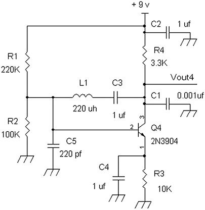
FIGURE 9-24 A common-emitter oscillator with multiple sections of lagging phase shift.
Transistor Q4 forms a common-emitter amplifier with C4, a l μF capacitor, to effectively AC ground the emitter of Q4. Note that choosing C4 too small, such as a 0.01 μF capacitor, will lead to “squegging,” where C4 at 0.01 μF causes a low-frequency oscillation that partially mutes out the oscillating signal. It was found the 1 μF for C4 produced reliable oscillations without “squegging.” However, if squegging (low-frequency chirping) occurs, C4 may be reduced to 0.1 μF.
The first stage of the approximately –90 degrees of phase shift is provided by C1 and R4, which produce a –3 dB cut-off frequency of about 48 kHz. The target oscillation frequency is about 750 kHz, so a roll-off from an RC filter at 48 kHz will ensure approximately –90 degrees of phase shift. The next stage of phase shifting is done via L1 and C5. DC blocking capacitor C3 ensures that L1 does not short the collector to the base of Q4 DC-wise, which will upset the DC biasing. The resonant frequency is determined approximately by:
![]()
where C is the series capacitance of C1 and C5, which is:
(1,000 pF × 220 pF)/(1,000 pF + 220 pF) = 180 pF
The output waveform is a distorted sine wave, as expected, because there is no AGC circuit here. About 2 volts peak to peak was measured at a frequency of approximately 790 kHz, which is pretty close to the calculation.
References
1. Ronald Quan, Build Your Own Transistor Radios. New York: McGraw-Hill, 2013.
2. Linear Circuits Data Book. Dallas, TX: Texas Instruments, 1984.
3. CMOS Logic Databook. Santa Clara, CA: National Semiconductor, 1998.
4. Paul R. Gray and Robert G. Meyer, Analysis and Design of Analog Integrated Circuits, 3rd ed. New York: Wiley, 1993.