
CHAPTER 11
![]()
Frequency Modulation Signals and Circuits
In Chapter 10, we explored some of the different types of amplitude-modulated (AM) signals such as amplitude modulation with carrier, suppressed carrier, and single sideband. The modulating signal such as a voice or music signal varied the amplitude of the carrier in standard AM, or it varied the amplitude of the sideband(s) of the suppressed carrier AM signal. Frequency-modulated (FM) signals do not vary the amplitude of the carrier signal. Instead, the actual frequency of the carrier changes according to the modulation signal. This chapter will look at broadcast FM signals and circuits for transmitting and receiving FM signals. Two broadcast FM radio projects will be presented, which should be workable for the reader, even though we are venturing into the very high-frequency (VHF) range of about 100 MHz.
What Are FM Signals?
See Figure 11-1 for an illustration of an FM signal. Figure 11-1 shows an FM signal where the positive peak of the low-frequency modulating signal (top waveform) causes the carrier signal (lower waveform) to increase in frequency, whereas the negative peak of the modulation waveform is at a minimum and causes the high-frequency carrier signal to decrease in frequency, as shown by the expansion in period of the high-frequency signal during that time.

FIGURE 11-1 An FM signal.
An FM signal can be characterized by the following equation:
![]()

Another way of expressing the FM signal is by the following equation:
![]()
We see that the carrier signal fc is varied over time by the factor of [1 + k m(t)], where m(t) is an alternating-current (AC) signal so that fc[1 + k m(t)] = fc + fc[k m(t)]. Since k m(t) is AC in nature, it has positive and negative numbers, ±kΔfc, which means that the instantaneous carrier frequency is fc ± kΔfc.
An example of a frequency-modulated (FM) signal is when one uses a signal generator and varies the frequency while having the amplitude set for a fixed level. Another example of frequency modulation is the sound of sirens or horns from a vehicle as it approaches you and goes away from you. The change in pitch is caused by the Doppler effect. In addition, when one listens to a violinist who applies vibrato by modulating the finger position on the neck of the violin, an FM effect occurs. Thus, when the frequency of a particular signal is changed with time, this leads to an FM signal.
For an FM broadcast signal, the carrier frequency is in the 100 MHz range, and the maximum deviation or shift in frequency at the carrier frequency is ±75 kHz. The modulation frequency ranges from 50 Hz to 15 kHz for the monaural channel known as the left plus right channel (L + R) and from 23 kHz to 53 kHz to form a double sideband suppressed carrier signal carrying the difference channel (L – R).
In AM signals, there are two aspects of the modulation signal. One is the amplitude of the modulation signal, which determines the depth of the amplitude-modulating effect on the carrier. The second is the frequency of the modulating signal, which determines the rate at which the AM signal’s carrier is varying with time.
For FM signals, there are also two aspects related to the modulating signal. One is the deviation in frequency from the nominal carrier frequency that is determined by the amplitude of the modulating signal. The higher the amplitude of the modulating signal, the higher is the frequency deviation. In a wideband FM channel, usually the maximum frequency deviation is approximately 75 kHz. For example, this means for a United States FM channel at 100.1 MHz, when the carrier is frequency modulated to its maximum, the carrier will vary from 100.100 MHz – 75 kHz to 100.1 MHz + 75 kHz. Stated another way, the radio station’s frequency varies from 100.025 MHz to 100.175 MHz. The second aspect of the modulating signal for FM is the frequency of the modulating signal that determines how “fast” the carrier swings back and forth.
From these two aspects, frequency deviation and modulation frequency, we can define two terms related to FM, which are the deviation ratio and the modulation index. The deviation ratio is the maximum peak-frequency deviation divided by the highest modulation frequency. A more general term is the modulation index, which is equal to the maximum peak-frequency deviation divided by a modulation frequency, which is less than or equal to the maximum modulation frequency.
In terms of sideband generation, the spectrum of an FM signal is different from an AM signal. In AM signals, the amplitude of the sidebands around the AM carrier is proportional to the amplitude of the modulating signals. Also, the sideband frequencies are just the sum and/or difference frequency such as fc ± fmod, where fc is the AM carrier frequency and fmod is the modulation frequency into the AM system.
However, in a (wideband) broadcast FM signal, the spectral content is much more complicated. The FM sidebands are generally a cluster of multiple sidebands whose frequencies are
ffm_carrier ± fmod
ffm_carrier ± 2fmod
ffm_carrier ± 3fmod
ffm_carrier ± 4fmod
That is, the sidebands include the first pair of sidebands like an AM signal but also include sidebands that are related to the harmonics of the modulating signal. The higher the frequency deviation, the more the higher-order sidebands are generated. Thus FM is not a linear process in terms of sideband generation, whereas AM has a linear relationship with its AM sidebands.
The actual analysis of FM sidebands takes a combination of higher-order mathematics including Taylor series expansion and Bessel functions. Fortunately, we will not cover this type of analysis in this chapter.
However, there is an approximation one can use to determine the bandwidth of an FM signal, which is Carson’s rule. The FM bandwidth BWFM, based on knowing the peak frequency deviation fpeak_deviation and the modulation frequency fmod is
![]()
For example, for an FM station with a peak frequency deviation of 75 kHz and a maximum modulation frequency of 15 kHz, the bandwidth is
BWFM = 2(fpeak_deviation + fmod) = 2(75 kHz + 15 kHz) = 2(90 kHz) = 180 kHz = BWFM
For analog TV signals, the audio FM carrier frequency after the video signal has been recovered in an analog TV tuner is 4.5 MHz in the United States. The maximum frequency shift or deviation is ±25 kHz, with typically a maximum modulating frequency of 15 kHz. Analog TV signals have been replaced with the digital TV transmission standard [e.g., Advanced Television Systems Committee (ATSC)], and therefore, FM audio signals are not used with TV signals except for some cable and amateur TV applications.
In the United States, the FM signal was invented by Edwin Armstrong as an alternative to amplitude modulation. FM signals have the advantage of providing higher-quality demodulation of the transmitted signal. This is true when the signal is fading in and out. In the case of an FM signal, once a sufficient level of the FM RF signal is received, for the most part, no fading is heard. In AM signals, fading or slow-moving changes in the strength of the AM signal cause an equivalent effect on the demodulated signal, which changes in volume.
For generating an FM signal, basically an oscillator is electronically varied in frequency, usually by a varactor or varicap tuning diode. There are other ways to achieve frequency modulation of an oscillator, such as electronic variable inductance (reactance modulator or electronically controlled gyrator), resistance-capacitance oscillators (e.g., an NE555 timer chip), or phase modulation. For this chapter, we will look at just using electronic tuning diodes as time-varying capacitors resonating with inductors to form tank circuits in LC oscillators.
Experiment No. 1: FM Oscillators Using Voltage-Controlled Capacitance Diodes
For a first experiment on frequency modulation, let’s build a low-power FM transmitter. This circuit will provide an FM signal within the FM band of 88 MHz to 108 MHz. An optional variable capacitor allows the transmit frequency to work below 88 MHz if desired (see Figure 11-2).
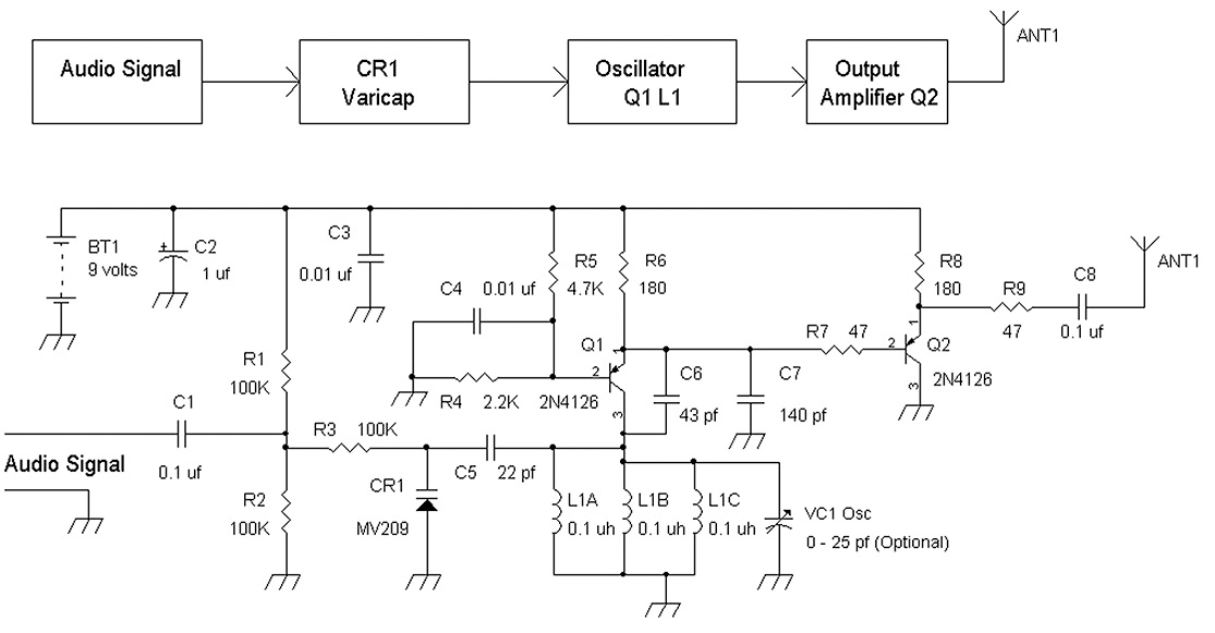
FIGURE 11-2 An FM oscillator with an MV209 tuning diode.
The FM oscillator in Figure 11-2 is a Colpitts oscillator using positive-feedback capacitors C6 and C7. With the values shown, the oscillation frequency is about 97 MHz. If the optional variable capacitor VC1 is installed, the carrier frequency can be lowered. For a ±75 kHz deviation or shift of the carrier frequency, an audio signal of about 350 mV peak to peak is connected to C1 and coupled over to varactor diode CR1 via R3. Varactor diode CR1, an MV209 tuning diode, provides the necessary voltage-dependent capacitance to electronically vary the oscillator’s frequency and generate the FM signal. Note that the cathode of MV209 is the lead on the right side when observing the flat portion of the TO-92 case with the leads pointing down.
Q1 forms a common-base amplifier via capacitor C4 providing an AC ground to its base. The collector current is set by voltage divider circuit R4 and R5 that places about +2.9 volts at the base of Q1. The emitter voltage is then 0.7 volts above the base voltage or +3.6 volts. Because the collector current is determined by the emitter current, which is the voltage across R6 divided by the resistance of R6, the collector current is then (9 volts – 3.6 volts)/180 Ω = 30 mA. The power across R6 is then I2R = (30 mA)2 × 180 Ω = 162 mW ≈ 1/6 watt. Although the suggested wattage rating for all resistors is ¼ watt, R6 and R8 would be better served with ½ watt resistors.
CR1 provides the variable capacitance for the FM effect and is reverse biased at about +4.5 volts. If more deviation is required, C5’s value can be increased. However, the carrier frequency will drop. Adding another inductor (e.g., 0.1 μH to 1 μH) in parallel with L1C will increase the carrier frequency. The output of the oscillator via Q1’s emitter is fed to an emitter-follower Q2 to provide a buffered FM RF signal. Buffering the RF signal provides stability to the oscillation frequency when the output terminal is connected to various antennas with different equivalent capacitances to ground. For example, hooking up an antenna straight to the emitter or collector of Q1 will cause the oscillation frequency to shift dramatically because of the parasitic capacitance of the antenna. Figure 11-3 shows a prototype breadboard of the circuit in Figure 11-2.
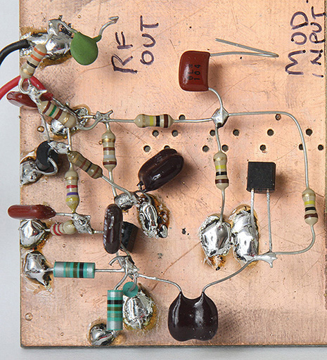
FIGURE 11-3 Prototype circuit of a Colpitts FM oscillator.
As mentioned in Chapter 5, power rectifiers also can be used as varactor diodes. Small amounts of voltage-controlled capacitance can be provided with just about any diode or rectifier. Chapter 5 suggested that power diodes can be used. For example, a 1N4002 diode does exhibit varactor diode characteristics. However, this 1-amp diode only provides small amounts of capacitance changes as a function of reverse-bias voltage. A larger-current diode such as the 1N5401 or 1N5402 provides variable capacitances comparable with some standard varactor diodes. Note that CR1 may be a 1N5400–1N5405 diode (see Figure 11-4).
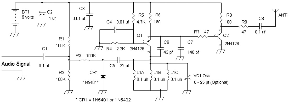
FIGURE 11-4 FM oscillator using a 1N5401 or 1N5402 power rectifier as the electronic tuning diode.
The 1N5401 or 1N5402 power rectifier will have somewhat less capacitance than the MV209, but nevertheless, it can provide an FM effect with less frequency deviation or shift than the MV209 varactor diode. To increase the frequency deviation while using the 1N5401 or 1N5402 power rectifier as a varactor, C5 can be increased from 22 pF to 100 pF or as high as 0.01 μF.
In both FM oscillators from Figures 11-2 and 11-4, using signals containing music may result in the sound being a little rolled off in the higher frequencies, but the circuits are adequate for voice transmission. With music, one will notice that both FM oscillators have a treble loss or treble cut when receiving the oscillator’s signal with a standard FM stereo receiver. The reason for this treble cut is that all FM stereo receivers have a built-in de-emphasis filter, which is a simple RC low-pass filter at 2.12 kHz (75-μs time constant, where μs = μsecond = microsecond).
Pre-Emphasis and De-Emphasis Transmitting and Receiving Equalization Curves
One of the characteristics of oscillators is phase noise. All oscillators have jitter or some time instability between each cycle of oscillation. For oscillators using crystals instead of inductors and capacitors, the phase noise is very low. But to generate an FM signal, inductor-capacitor oscillators are used. If a phase detector is used to convert the phase noise into a voltage, we will find, for example, that the noise from the output of the phase detector is flat in frequency spectrum. However, if we use a frequency-modulation detector instead, we will find that the noise voltage out of the FM detector is a boosted at high frequencies. This is equivalent to having the same noise from the phase detector with an added audio middle- to high-frequency boost.
That is, when any FM demodulator is used prior to a de-emphasis network, such as the FM detector in your stereo receiver or tuner, that FM detector adds a treble boost to white noise (flat frequency spectrum noise) (see Figure 11-5). Notice that the noise spectrum shape from an FM detector has a rising or upward ramp emphasis, which is commonly called a triangular-noise spectrum.
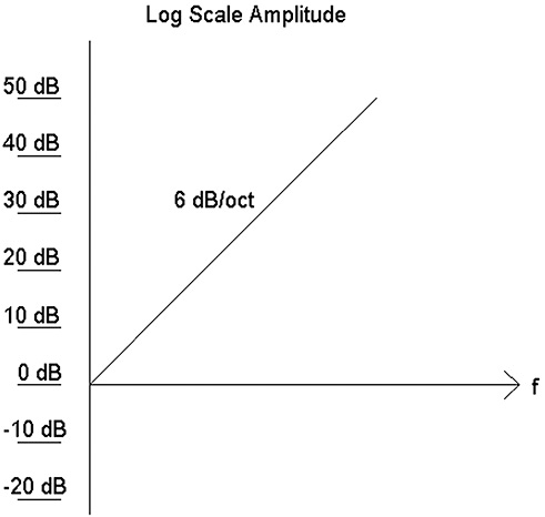
FIGURE 11-5 Noise spectrum from the FM detector on a zero-modulation FM carrier with random phase noise.
If we apply a simple low-pass filter after the FM detector, we get to attenuate the noise by reshaping the triangular noise spectrum back to mostly a flat noise spectrum (see Figure 11-6). However, if we now decide to modulate the FM transmitter with signals beyond the cut-off frequency of the simple RC filter after the FM demodulator, the frequency response of the transmission will suffer accordingly and roll off (see Figure 11-7).

FIGURE 11-6 Simple RC filter to transform the triangular noise spectrum back to a mostly flat noise spectrum.
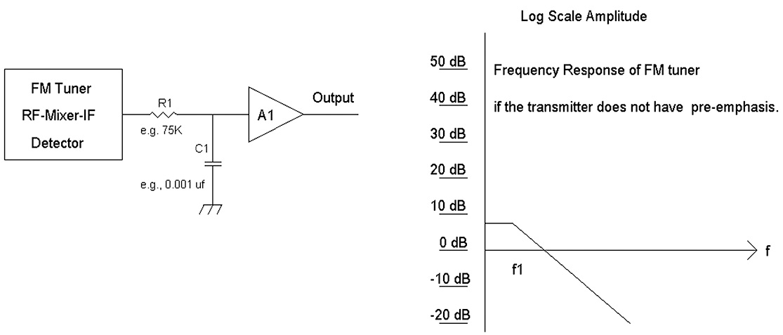
FIGURE 11-7 Frequency response with an RC filter on the receive side to reduce triangular noise.
In one sense, we “fixed” the noise problem on the receiving end of the FM oscillator but caused another problem by having the demodulated FM signal suffer with a treble cut frequency response. So how do we get out of this mess? We can add a treble boost to the audio signal prior to its being frequency modulated. For example, if the RC filter at the receiver end has a 75-μsecond time constant for the roll-off at 2.12 kHz, we use an RC treble boost filter circuit to boost the treble starting at 2.12 kHz for the modulating signal at the transmitter end to cancel out the roll-off on the receiving end.
The treble boost at the FM modulator or transmitter side is called pre-emphasis, and the treble cut or low-pass filtering at the receiver is called de-emphasis. Figure 11-8 presents pre-emphasis and de-emphasis equalization curves. Note that the “corner frequency” for the boost (f1) at the transmitter side must be matched at the receiver side in order to maintain a flat response for the received modulating signal.
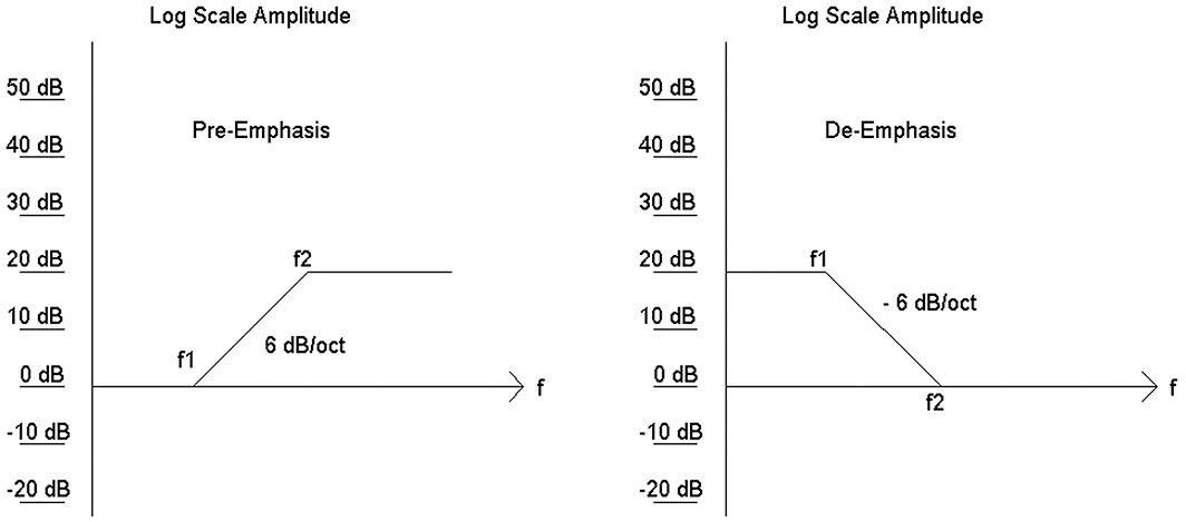
FIGURE 11-8 The transmitter’s pre-emphasis and receiver’s de-emphasis frequency responses.
Observing the Pre-Emphasis and De-Emphasis Effect
To get a feel of what pre-emphasis and de-emphasis equalization sounds like, see Figure 11-9. This figure shows two different input signals, a noise source and an audio source. For the noise source, one can use an FM radio that is tuned to a frequency where there are no stations. For example, tune to “blank” stations at either end of the FM dial (e.g., near 88 MHz or 108 MHz), which will produce hiss. The level of hiss can be adjusted via the volume control of the radio. For the audio source, another radio or a CD, DVD, or MP3 player can be used. The output is fed to an audio amplifier connected to a loudspeaker or to a high-fidelity headphone or earphone.
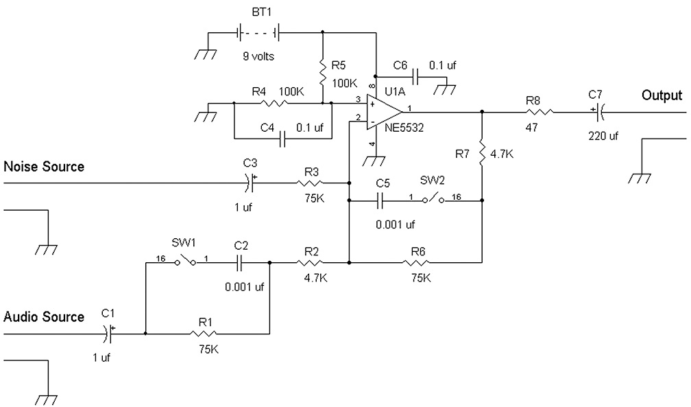
FIGURE 11-9 Experiment with pre-emphasis (via SW1 turned on) and de-emphasis (via SW2 turned on) networks.
Switch SW1 enables the pre-emphasis or treble boost, and SW2 turns on the de-emphasis or treble cut. With noise added to the audio (music) source, turn off both SW1 and SW2, and listen to the amount of noise in the background of the music. Now turn on both SW1 and SW2, and you should not notice a change in fidelity, but the noise level should be lower. R8 can vary from about 22 Ω to 220 Ω to change the overall audio level to the headphones. If you want to listen to just pre-emphasis, turn SW1 on and SW2 off. And turning SW1 off and SW2 on will let you listen to what de-emphasis sounds like to a flat frequency-response signal.
FM and a Pre-Emphasis Network
Pre-emphasis of the audio signal is achieved by adding an RC network. See Figures 11-10 and 11-11. With the addition of R10 (91 kΩ), R11 (12 kΩ), and C9 (820 pF) in Figure 11-10, the modulator now has a pre-emphasis network. R11 (12 kΩ) via AC “short” C1 is in parallel to R1 (100 kΩ) and R2 (100 kΩ), which results in a total resistance of about 9.7 kΩ. The first time constant τ1 for the pre-emphasis is
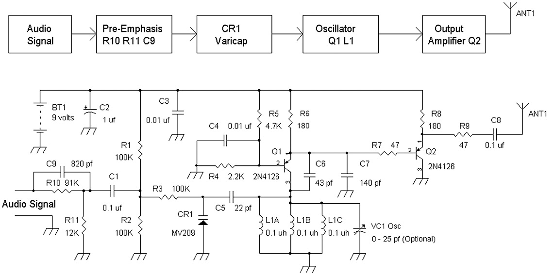
FIGURE 11-10 Two-transistor FM modulator with pre-emphasis network.

FIGURE 11-11 FM modulator with pre-emphasis network, inverter gates, and 1N5401/1N5402 varactor diode.
τ1 = R10C9 = (91 kΩ)820 pF = 74.6 μseconds ≈ 75 μseconds,
which starts a treble boost at 2.12 kHz. The second time constant τ2 is where the treble boost flattens out, and this is
τ2 = (R10||9.67 kΩ)820 pF = (8.74 kΩ)820 pF = 7.16 μseconds
or a flattening out at about 22 kHz.
At frequencies below 2.12 kHz, the network acts like a 1/10 attenuator. The network eventually has a gain of approximately 0.707 at 22 kHz. Therefore, more signal is required to drive this modulator, something like 1 volt RMS AC or about 2.8 volts peak to peak. Most CD or DVD players will output this signal level.
A similar pre-emphasis network is provided by R1, C1, and VR1 in Figure 11-11. There is some parallel resistance with R2 and VR1, but this can be ignored, and the time constants are
τ1 = R1C1 = (91 kΩ)820 pF = 74.6 μseconds ≈ 75 μseconds
which starts a treble boost at 2.12 kHz. Then:
τ2 = (R1||10 kΩ)820 pF = (9.0 kΩ)820 pF = 7.38 μseconds
which flattens out at about 21.5 kHz and is essentially the same as the pre-emphasis network of Figure 11-10. Now see Figure 11-11, CR1.
This oscillator uses a power rectifier 1N5401 or 1N5402 as the varicap diode. Again, the diode CR1 is reverse biased, so there is close to infinite resistance looking into the anode of CR1 at audio frequencies. The oscillator uses a logic inverter gate U1A and is direct-current (DC) biased via R4 and L1A to use the logic inverter gate as an inverting amplifier. Oscillation occurs because the phase-lag network via R4 and C8 adds negative phase shift to the phase-lag network of L1A and C6 in parallel with VC1 and the series capacitance of C5 and voltage-controlled capacitance of CR1. This type of oscillator takes at least a few minutes to stabilize in frequency, and the 7805 voltage regulator U1 ensures a stable power-supply voltage to minimize frequency drift. Full ±75-kHz frequency deviation is achieved by applying about 2.8 volts RMS (8 volts peak to peak) at the audio signal input terminal and turning VR1 to maximum.
The output of U1A is then buffered with logic inverter U1B, which then is coupled to the antenna. This oscillator circuit will also emit harmonics of approximately 200 MHz, 300 MHz, and beyond. With VC1, a trimmer variable capacitor set to minimum capacitance, the approximate oscillation frequency is 94 MHz. A higher frequency can be achieved by paralleling an inductor between 0.33 μH and 3.3 μH across L1A. An oscillator using a 74AC04 gate has a “top speed” or oscillation frequency in excess of 150 MHz. Figure 11-12 shows a prototype breadboard of the 74AC04 FM oscillator without the pre-emphasis network.

FIGURE 11-12 Prototype breadboard of the 74AC04 FM oscillator without the pre-emphasis network.
FM Radios
Unlike AM radios that can be implemented in a non-superheterodyne manner such as a crystal, TRF, superegenerative, reflex, or regenerative radio, FM radios from the beginning of commercial manufacture were superheterodyne in nature. Yes, there are some rare designs that use a superregenerative architecture, but these designs are generally sold only as hobbyist kit radios.
Virtually all commercially available FM radios come from a superheterodyne circuit (see Figure 11-13). The basic FM radio has many common elements with the AM superhet. For example, there are the local oscillator, mixer, intermediate-frequency (IF) amplifier, and audio circuits. In many FM receivers, there are no AVC (automatic volume control) systems such as the ones that are common in AM superhet radios. Generally, the last IF amplifier causes the IF signal to limit its amplitude. This can be done with a differential-pair amplifier to ensure that the waveform is a symmetrical squarewave signal that will be inputted to the FM detector. By presenting a clipped sine wave that is transformed into a squarewave, any small amplitude variation that causes fading of the RF signal between the transmitter and receiver is processed to be ignored by the limiter or clipping amplifier.

FIGURE 11-13 Block diagram of a superheterodyne FM radio.
In terms of a receiving antenna, there are no air-core or ferrite-core antenna coils as used in AM radios. Instead, most FM radios use a wire antenna in the form of a telescopic whip antenna or a piece of wire at least 6 inches long. Another difference in the FM radio is that there are generally more IF stages in terms of amplifiers and IF filters than those found in AM radios. The reason is that the signal from the wire antenna is very low in strength compared with the signal from an AM antenna coil. For example, a ferrite-bar antenna may output millivolts of RF signals, while the FM antenna will generally receive only tens of microvolts. In an AM radio, one IF amplifier stage with one or two IF filters will suffice. But in an FM radio, at least two stages of amplification are needed with two IF filters.
Most AM radios did not have an RF amplifier stage. For an FM radio, an RF amplifier, generally a common-base stage, provided isolation from the local oscillator such that the wire or telescopic antenna did not radiate signals from the oscillator circuit.
Finally, the most important distinguishing feature of an FM radio versus its AM counterpart is the detector or demodulator. AM radios use simple diode rectification or power detectors to recover the envelope information of the amplitude-modulated signal. In FM radios, however, the IF signal should have no form of amplitude modulation. Therefore, standard AM detectors will generally not work for demodulating the FM signal straight from the IF filter.
What most FM detectors (e.g., stagger tuned, Foster Seeley FM discriminator, differential peak, and ratio detector) do is to first convert the FM signal into an AM signal and then use the diodes as half-wave rectifiers to recover the audio signal. We will look into some more details of the different types of FM detectors later in this chapter.
In summary, differences between FM and AM radios include
• There are tuned RF stages in FM radios, whereas AM radios typically run the RF signal to the converter or mixer directly.
• There are generally more IF amplifiers and IF filters in FM radios than in AM radios.
• FM detectors are more complicated and use simple AM detection only after converting the FM signal into an AM signal.
• Telescopic or wire antennas are used to capture the FM signal versus using antenna coils for AM radios.
Historically, in the 1950s and 1960s, commercially manufactured transistor FM radios were hardly ever sold as FM-only radios. One example in 1963 is that Hitachi made a nine-transistor radio, the KH-915, that was FM only. This radio had an RF amplifier, three stages of IF amplification, three 10.7 MHz IF transformers, and a ratio (FM) detector. However, almost all radios that had FM also had AM, and some added shortwave (SW) as well.
Let’s take a look at a multiband portable AM-SW-FM radio from the late 1960s, the Ross Model RE-1915-N. Figure 11-14 is a partial schematic of the radio showing the FM section. As shown in the RE-1915-N AM-FM-SW radio schematic transistor, Tr.1 is a grounded base amplifier that receives the RF signal via a telescopic rod antenna into the emitter. Because the antenna is a low-impedance voltage source and is connected directly to the parallel inductor-capacitor circuit with L1 and capacitors, the bandwidth is actually large enough to cover the entire frequency range of 88 MHz to 108 MHz.
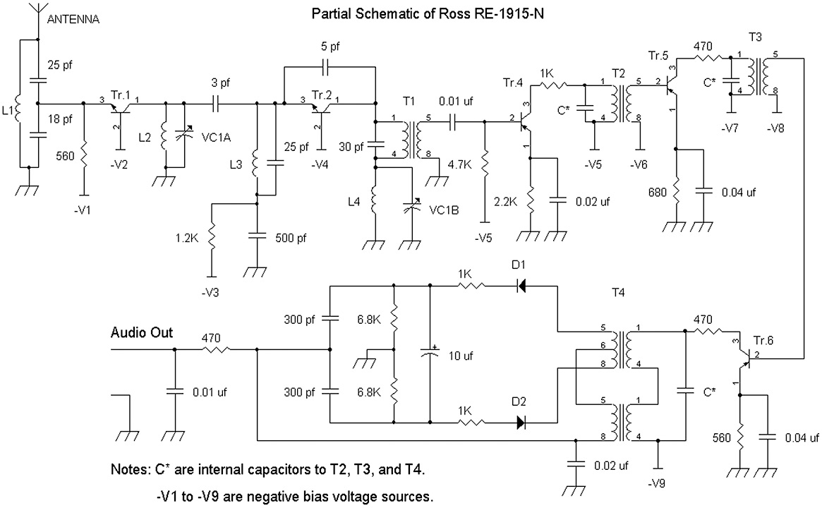
FIGURE 11-14 A partial schematic diagram of a Ross RE-1915-N radio.
The collector (current source) output of Tr.1 is then connected to a tunable RF filter formed by the FM RF variable capacitor section that is in parallel with inductor L2. In order to preserve the Q, or quality, factor of this parallel LC circuit, a small-valued 3 pF capacitor is used to couple the amplified tuned RF signal from the collector of Tr.1 to the emitter of Tr. 2, an oscillator-mixer circuit otherwise known as a converter circuit. By using the 3 pF coupling capacitor, loading on the tuned RF tank circuit with L2 is minimized, and as the RF section variable capacitor is tuned across the FM band, good variable-frequency band-pass filtering is achieved. This band-pass filtering is essential for rejecting out-of-FM band signals and for providing image rejection.
Transistor Tr.2 is a variable-frequency Colpitts oscillator with the FM oscillator section of the variable capacitor in parallel with inductor L4. The collector of Tr.2 is connected to positive-feedback capacitors whose values are 5 pF across L4 and emitter and a 25 pF capacitor from the emitter to a large-valued 500 pF capacitor. The other end of the 500 pF capacitor is tied to ground. The collector of Tr.2 is also connected to 10.7 MHz IF transformer T1 that extracts the difference-frequency signal (fosc – fRF) = fIF = IF = 10.7 MHz.
NOTE fosc = oscillator frequency, fRF = tuned RF frequency, and fIF = intermediate frequency or IF.
Before leaving the Tr.2 circuit, let’s take a look at two components. Inductor L3 has one side connected to the emitter and the other side connected to the 500 pF capacitor whose other lead goes to ground. Note that the amplified tuned RF signal from Tr.1 is coupled to L3 via the 3 pF capacitor. So what are we getting into with these two components, L3 and the 500 pF capacitor? Seems like the amplified tuned RF signal would be singing, “We’re caught in a trap,…” but I’m just kidding about the song—although one may “suspect” that I may have been listening to too much music … enquiring minds and suspicious minds would like to know—just kidding again!
However, in reality, the amplified RF signal is going into a 10.7 MHz or IF signal-band reject filter, aka a 10.7 MHz trap circuit. L3 and the 500 pF capacitor form a series resonant circuit that has close to zero impedance at 10.7 MHz at the input of the Tr.2 converter circuit to notch or short out any signal at or near 10.7 MHz. At the FM band frequencies of 88 MHz to 108 MHz, L3 and the 500 pF capacitor have little effect and pass signals related to the FM band.
There are two good reasons for having a notch filter prior to the input of the converter. One is so that 10.7 MHz signals from other FM radios will not leak through the RF front-end circuit and, second, because there are multiple stages of IF amplifiers that deliver very high voltage gains at 10.7 MHz. The 10.7 MHz trap reduces the chance that IF signals can oscillate by leaking back to mixer Tr.2, which is still an amplifier.
Moving on, we now need to amplify the IF signals. In this radio, Tr.4, Tr.5, and Tr.6 form a three-stage IF amplifier system. IF transformers T1, T2, and T3 provide band-pass filtering at 10.7 MHz. The alternate channel selectivity (amount of attenuation 400 kHz away from 10.7 MHz) is about 12 dB per stage. With three stages, the alternate channel selectivity is about 36 dB. For most instances, 36 dB is acceptable but will have trouble separating close-by stations.
What I would like to share with you is that just by adding one more IF amplifier and IF filter, this radio would be improved immensely. The selectivity will go from about the mid-thirties to the middle to high forties decibel (dB)wise, which then allows very good separation of closely packed FM stations. The sensitivity also will go up. Better yet, instead of using an extra IF transformer, use a 10.7 MHz ceramic filter to take the selectivity >50 dB, which is then comparable with high-quality stereo tuners selectivity-wise.
We now turn to the FM detector of the RE-1915-N radio, which is a ratio detector, via T4, a special ratio detector transformer with four windings. Basically, this type of detector works on two principles:
1. One of the windings has a 90-degree phase-shifted 10.7 MHz IF signal when compared to a reference winding that is defined to have 0 degrees when the 10.7 MHz IF signal has no FM modulation.
2. As the 10.7 MHz IF FM signal shifts below and above the nominal 10.7 MHz frequency, there are added and subtracted phase shifts from the 90 degrees. For example, at 10.65 MHz, the phase shift is 105 degrees; at 10.70 MHz, it is 90 degrees; and at 10.75 MHz, the phase shift is 75 degrees. In this case, the subtracted and added phase shifts are +15 degrees and –15 degrees or +φ and –φ, where φ is the added or subtracted phase shift to the 90-degree signal.
Eventually, the two signals, the reference 0-degree signal and the second signal that has 90 degrees minus or plus the phase shift, φ, are added together.
By way of a graphing calculator, let’s see what happens to the amplitude of the added signals for ±15 degrees (see Figures 11-15 and 11-16). That is, let’s plot the resulting amplitudes for the following three signals:
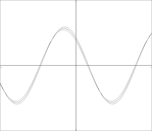
FIGURE 11-15 Resulting amplitudes of cosine waveforms with 0 degrees summed with 75, 90, and 105 degrees from largest to smallest amplitudes. Waveform in the middle is 0 degrees summed with exactly 90 degrees.
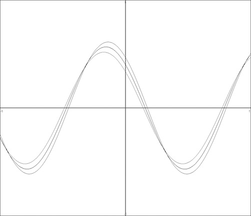
FIGURE 11-16 Resulting amplitudes of cosine waveforms with 0 degrees summed with 60, 90, and 120 degrees from largest to smallest amplitudes. Waveform in the middle is 0 degrees summed with 90 degrees.
• cos(x) + cos(x + 90 degrees – 15 degrees) = cos(x) + cos(x + 75 degrees)
• cos(x) + cos(x + 90 degrees)
• cos(x) + cos(x + 90 degrees +15 degrees) = cos(x) + cos(x + 105 degrees)
As seen in Figure 11-15, the waveforms are of three different amplitudes with combinations of
• Largest amplitude: cos(x) + cos(x + 75 degrees)
• Middle amplitude: cos(x) + cos(x + 90 degrees)
• Smallest amplitude: cos(x) + cos(x + 105 degrees)
Intuitively, this makes sense. The phase-shifted cosine waveform closest to 0 degrees, which is 75 degrees, will be the largest one because two waveforms of 0 degrees will just add normally like two positive numbers.
The waveform furthest away from 0 degrees would be the one closest to 180 degrees and should be the smallest because equal amplitude waveforms of 0 degrees and 180 degrees added together would cancel out to a zero amplitude waveform. Figure 11-15 shows the amplitudes of an FM detector prior to half-wave rectification for a 15-degree phase-shift example. Suppose that the 10.7 MHz IF signal shifts are 30 degrees of phase shift for a deviation of 100 kHz instead of the 50-kHz example? And suppose that we get twice the phase shift from 90 degrees to have 120, 90, and 60 degrees for 10.6 MHz, 10.7MHz, and 10.8MHz? See Figure 11-16.
As we can see, increased frequency deviation of the IF signal will result in the ratio detector’s 90-degree phase-shifting circuit to also increase the amount of phase shift added to the 90 degrees. In Figure 11-15, we see that the ratio detector’s phase-shifting network “maps” frequency shift or frequency modulation to amplitude variations or amplitude modulation. For example, in Figure 11-16 the largest cosine waveform represents the IF signal shifted to 10.80 MHz, the middle-amplitude waveform represents the IF at 10.70 MHz, and the smallest waveform represents the IF signal shifted to 10.60 MHz.
A simple representation of converting the addition of the phase-shifted and non-phase-shifted signals is given in Figure 11-17. As shown in the figure, there is a 90-degree phase-shifting network that includes a series resonant circuit R1, C1, L1, and L2. At the IF (intermediate frequency) of 10.7 MHz, the nominal phase shift at L1 and L2 is 90 degrees. L1 and L2 form a voltage divider of approximately 1/30 because “gain” of the circuit at C1/L1 is about 30 at the resonant frequency. The phase-shifted signal and the reference FM signal V_IF are added together via the summing circuit. The output of the summing circuit produces an amplitude-modulated signal such as the amplitude variations seen in Figure 11-15. The amplitude-modulated signal is then detected or demodulated with an envelope detector circuit CR1, R2, and C2 to provide the recovered modulating signal such as audio (e.g., voice, music, etc.). It should be noted that the 90-degree phase-shifting circuit must provide additive and subtractive phase shifts outside the resonant frequency.

FIGURE 11-17 Conceptual diagram of converting FM to AM via a phase-shifting network.
NOTE If the phase shift were to be the same for all frequencies at the resonant frequency and above and below the resonant frequency, the output of the summing circuit would be a constant-amplitude waveform, free of amplitude modulation and hence free of any demodulated signal.
A balanced AM detector circuit is shown in Figure 11-14 as diodes D1 and D2. There are two diodes to provide a push-pull or balanced FM detection curve, which allows for providing 0 volts when the IF frequency is at 10.7 MHz and positive or negative voltages to output a demodulated audio signal when FM is present in the IF signal.
Historically, the ratio detector was the last of the double-tuned circuits required to demodulate FM signals. By the time FM was used for the sound portion of analog television receivers, the TV sets did have double-tuned FM detectors, but as a cost savings, eventually a single-tuned circuit was used for FM demodulation, called the quadrature FM detector.
For the next project, we will present an FM radio project in which a quadrature detector is used.
An FM Tuner Project with Ceramic Filter and Resonator
This circuit uses a minimum of adjustable coils or IF transformers. Instead, it will rely on one or more ceramic filters for the 10.7 MHz IF amplifier system and a 10.7 MHz discriminator ceramic resonator for the quadrature detector inside the TA2003 integrated circuit (IC) (Figure 11-18).

FIGURE 11-18 An FM tuner circuit with minimal coils and no IF transformers.
Parts List
• C1 is optional (1 pF to 22 pF) but may not be needed because of VC1A Pad, which has a 0 pF to 20 pF range.
• C2, 15 pF ceramic or silver mica 5% or 10%
• C3, C4, C6, C7, 0.001 μF, 5% or 10% ceramic or film capacitor
• C5, C9, 1 μF, 5% to 20% film or ceramic capacitor
• C8, 0.047 μF, 5% film capacitor
• CR1, 1N4002 or any 1N4000 Series rectifier
• L1, L2, 0.1-μH, 5% or 10% fixed or variable inductors
• Unless specified, all resistors are ¼ watt, 5%
• R1, 100 Ω
• R2, 1 kΩ
• VC1A, VC1B, a twin-gang variable capacitor 0 pF to 20 pF with two 0 pF to 20 pF pad capacitors
• Y1, 10.7 MHz ceramic resonator-discriminator (Murata Part Number CDALF10M7GA048-B0 or, alternatively, Murata Part Number CDALF10M7GA040-B0)
• Mouser part numbers, respectively, are 81-CDALF10M7GA048-B0 and 81-CDALF10M7GA040-B0 (www.mouser.com); an alternative part from www.digikey.com is the CDALF10M7GA096-B0
• F1, 10.7 MHz ceramic filter by Murata or Toko with a –3 dB bandwidth of 150 kHz to 280 kHz at 330 Ω (available at www.digikey.com or www.mouser.com)
• Typical part numbers are SFELF10M7LFTA-B0 (280 kHz) and SFELF10M7JAA0-B0 (150 kHz)
NOTE Markings on the ceramic filter may vary and one should read the datasheet for the pin out identification.
• U1, TA2003 IC (integrated circuit) (Toshiba or UTC, Unisonic Technologies)
• BT1, 3 volt source via two 1.5 volt batteries
Figure 11-18 shows an easier-to-build FM radio as opposed to the one shown in Figure 11-14, which uses many adjustable parts such as IF transformers and a two-ferrite-core ratio detector transformer. With just the twin 20 pF tuning capacitor and its trimmer capacitors (pad capacitors), there are no other adjustments for the circuit shown in Figure 11-18. The IF filter is a ceramic filter. One can choose for sharper selectivity by using a 150-kHz bandwidth filter. However, the tuning may be too sharp. Typically, a 230-kHz or 280-kHz filter is used, and if two or more are connected in series to deliver much better alternate channel selectivity, multiple 280-kHz filters are recommended (see Figures 11-19 and 11-20).

FIGURE 11-19 Improving selectivity by cascading two ceramic filters F1 and F2 (same type 10.7 MHz filters as mentioned in the Parts List).

FIGURE 11-20 A TA2003 FM tuner with two ceramic filters.
The radio receives the RF signal via antenna ANT1, which is fed to pin 1 of the TA2003 chip via C4. The RF amplifier has a collector output that drives a tunable parallel inductor-capacitor tank circuit VC1A and L1. The amplified RF signal is coupled to a separate RF mixer. The local oscillator tank circuit is formed by L2 and VC1B. Tuning the local oscillator frequency is accomplished by VC1B, and the output of the oscillator is connected to the RF mixer. The “balanced” RF mixer in the TA2003 is more sophisticated than a simple one-transistor mixer used in AM radios.
A single-transistor RF mixer not only outputs the IF signal and the RF signal, but also the oscillator signal. However, the oscillator signal is generally the largest signal from the output of the single-transistor RF mixer or converter circuit. Generally, a ceramic filter cannot be connected directly to the output of the single transistor because the large-amplitude oscillator signal will leak through the ceramic filter. Instead, prefiltering is required, and an LC filter via an IF transformer must precede the ceramic filter.
The Gilbert mixer used in the TA2003 has at least four transistors that form a multiplier circuit to provide the IF signal while balancing or nulling out the oscillator signal. From the mixer’s output connected to ceramic filter F1, the IF signal is amplified and sent to an FM detector, which is a quadrature detector. Ceramic resonator Y1 is essentially a 10.7 MHz band-pass filter resembling a parallel LC circuit. Y1 provides two characteristics to the 10.7 MHz IF signal, one is a 90 degree phase-shift signal at 10.7 MHz, and the other is a phase-shift signal in degrees below and above the 10.7 MHz IF, which varies and can be characterized as (90 + φ) and (90 – φ). For quadrature detection to occur, the non-phase-shifted signal and the phase-shifted signal are multiplied, which results in a signal that demodulates the FM signal. The math behind this involves sines and cosines and other trigonometric functions. Figure 11-21 provides a conceptual diagram of the quadrature FM detector.
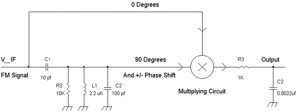
FIGURE 11-21 Example of an FM quadrature detector.
A quadrature detector is illustrated in Figure 11-21. A multiplying circuit receives 0- and 90-degree signals from the IF amplifier. By multiplying the two signals, the additive and subtractive phase shifts caused by the IF signal shifting outside the resonant frequency (e.g., above and below or below and above 10.7 MHz) form a demodulated FM signal at the output of the multiplying circuit (e.g., NE602, SA612, or MC1496). The high-frequency “junk” that comprises signals at multiples of the intermediate frequency (IF) is filtered out by R3 and C2, leaving only signals from about 20 Hz to about 80 kHz. The 80-kHz bandwidth is required to receive the main audio channel signal from 50 Hz to 15 kHz, the stereo difference channel signal from 23 to 53 kHz, and any other signal up to about 76 kHz.
Now let’s look more closely at the LC circuit (see Figure 11-22). Typically, in quadrature detectors, a 90-degree phase-shifter circuit is implemented by converting a parallel resonant circuit that normally has 0 degrees of phase shift at the resonant frequency into a series resonant circuits that has a 90-degree phase shift. At first glance, it would appear that we are only dealing with parallel resonant circuit L1 and C2. But, on closer inspection, we see that it is driven by a small-value (high-impedance) capacitor. If we just look at the LC circuit, we find out that we can make a Thevenin equivalent circuit of C1, C2, and V_IF.

FIGURE 11-22 A Thevenin equivalent LC circuit from parallel to series resonant.
From the dashed lines shown on the left side circuit in Figure 11-22, we can “separate” the LC circuit and rearrange it as a capacitive voltage divider of C1 and C2. This capacitive voltage divider circuit then drives R2 and L1. But the capacitive divider can be seen as a Thevenin equivalent circuit as a voltage source divided down by (the voltage dividing effect of) C1 and C2 and, more important, as an equivalent series capacitor C1 || C2 that is driving R2 and L1. Thus, by capacitively coupling the LC circuit of L1 and C2 with C1, we actually get the equivalent of a series resonant circuit, which then provides the required 90-degree phase shift plus additive and subtractive phase shifts from the 90 degrees when the IF is outside the resonant frequency (e.g., 10.7 MHz). As we observe the series resonant circuit on the right side of Figure 11-22, we see that it is a high-pass filter that has a high Q factor (e.g., narrow bandwidth around the resonant frequency). The phase shift is leading to +90 degrees at the resonant frequency. Also note that C1 is generally 10 percent or less of C2. Note that R2 determines the Q of the circuit, and for wider-band FM detection, R2 should be lowered in value (e.g., 1 kΩ < R2 < 10 kΩ).
Similarly, we can use a large-value inductor (high impedance) in series with a parallel LC circuit to also make a 90-degree phase shifter (see Figure 11-23). As seen in Figure 11-23, we can again form the series-driven LC circuit as an inductive voltage divider to form a Thevenin equivalent circuit. This Thevenin equivalent circuit is shown on the right side of Figure 11-17b, which shows a series resonant circuit forming a high Q low-pass filter. Again, there is a 90-degree phase shift with this circuit, but the phase shift is lagging. Thus, at the resonant frequency, the phase shift is –90 degrees. For choosing the value of L2, normally it has at least 10 times the inductance of L1. Note that R2 determines the Q of the circuit, and for wider-band FM detection, R2 should be lowered in value (e.g., 1 kΩ < R2 < 10 kΩ).

FIGURE 11-23 An extra inductor L2 is used to transform a parallel resonant circuit to a series resonant circuit.
A Second FM Radio Project Via Silicon Labs
Making FM radios for the do-it-yourself (DIY) hobbyist can be very challenging because of the very high frequencies involved. I deliberately avoided showing as projects the more “traditional” FM radios using discrete transistor designs with IF transformers and ratio detector coils. The alignment procedure for these types of radios requires sweep generators, calibrated FM modulators, oscilloscopes, and possibly spectrum analyzers. Also, it is very hard to obtain ratio detector coils easily unless one buys an FM radio kit such as those available from www.elenco.com via this specific link from Elenco: www.elenco.com/product/productdetails/radio_kits=MTc=/am--fm_radio_kit(combo_ic_&_transistor)=NTk1.
Therefore, a really easy FM radio project that also includes the capability to add an AM section for standard broadcast and shortwave bands can be implemented via a Silcon Labs 4836 chip, which is available at www.mouser.com. This IC (integrated circuit) is only available in a standard small outline surface-mount form factor, but it can be soldered to a 16-pad adapter board for easy access to the 16 pins. The original prototype was built on copper-clad with the chip “floating” above the copper ground plane. Figure 11-24 shows the schematic.
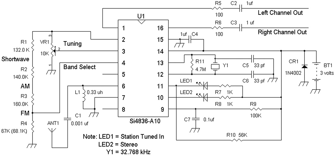
FIGURE 11-24 Silicon Labs FM stereo tuner schematic.
Parts List
• C1, 0.001 μF, 5%, 10%, or 20% ceramic or film capacitor
• C2, C3, C4, 1 μF, 5% or 10% film or ceramic capacitor
• C5, C6, 33 pF, 5% or 10% ceramic or silver mica capacitor
• C7, 0.1 μF, 5%, 10%, or 20% ceramic or film capacitor
• L1, 0.33 μH, 5% or 10% inductor (alternatively, L1 can be any fixed inductor between 0.27 μH and 2.7 μH)
• R1, 132 kΩ, 1% or 133 kΩ 1% resistor
• R2, 140 kΩ, 1% resistor
• R3, 160 kΩ 1%, 162 kΩ 1%, or 158 kΩ 1% resistor
• R4, 67 kΩ 1%, 66.5 kΩ 1%, or 68.1 kΩ 1% resistor
• R5, R6, 100 Ω, 5% resistors
• R7, R8, 1 kΩ, 5% resistor
• R9, 100 kΩ, 5% resistor
• R10, 56 kΩ, 5% resistor
• R11, 4.7 MΩ, 5% resistor
• Y1, watch crystal, 32.768 kHz
• CR1, 1N4002 rectifier or any 1N4000 series diode
• BT1, 3 volt source from two batteries such as two AA cells
• LED1, LED2, any green, yellow, or red (preferably high-brightness) light-emitting diodes (LEDs) Note: Do not use a white or blue LED because the power supply is already 3 volts, and these LEDs require at least 3 volts to turn on brightly.
• U1, Silicon Labs IC (integrated circuit) Si4836-A10
• VR1, 10-kΩ pot, single turn
NOTE The schematic shown in Figure 11-24 is different from the data sheet circuit of the Si4836 chip. The data sheet shows that the 32.768-kHz crystal oscillator circuit is optional. However, it is not. If the radio is built without the crystal oscillator circuit Y1, C5, C6, and R11, the radio will not work. Hence the crystal oscillator circuit is essential.
From the schematic of the demo board, the extra parts Y1, C5, C6, and R11, along with the LEDs and R10, are shown and are to be loaded. Once the parts are connected as shown in Figure 11-24, you should be able receive FM stations in stereo. This chip uses the latest software-defined radio techniques as of the year 2013. The RF signal is mixed down to form 0 degree and 90 degree signals, which are converted via two analog-to-digital converters into a digital signal processor to set the bandwidth of the IF and demodulate the FM signal all in the digital domain. Two digital-to-analog converters provide left and right channel analog audio outputs.
Tuning and band selection are accomplished by a variable resistor and a voltage divider circuit. As shown in the figure, a four-resistor voltage divider circuit via R1, R2, R3, and R4 provides various voltages to select shortwave, AM, or FM bands. Tuning is accomplished via a single 10 kΩ potentiometer or variable resistor.
This schematic is just for receiving FM stations. To receive shortwave and AM signals, an antenna coil is required. The spec sheet can be downloaded at www.silabs.com/Support%20Documents/TechnicalDocs/Si4836-A10.pdf, and the demo board information can be found at www.silabs.com/Support%20Documents/TechnicalDocs/Si4836DEMO.pdf. As with the Si4836 and TA2003 tuners, the audio output should be connected to an audio power amplifier such as an LM386 circuit or to a stereo amplifier.
When one sees the Silicon Labs tuner chip and compares it with the tuner section (mid-1960s circuit design) in Figure 11-14, a radio that uses discrete transistors, coils, variable capacitors, IF transformers, ratio detector coils, one sees that progress certainly has been made over the span of 50 years in radio technology.
Figure 11-25 shows a prototype breadboard of the Silicon Labs FM tuner, and Figure 11-26 shows some surface-mount IC adapters that can be used to more easily use the Silicon Labs Si4836 surface-mount SO-16 IC (integrated circuit).

FIGURE 11-25 Prototype radio using the Si4836 chip that is “hanging” in midair.
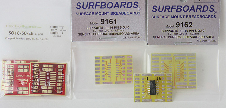
FIGURE 11-26 Various surface-mount IC adapter boards.
The adapter boards in Figure 11-26 are from ElectroBoards and SURFBOARDS. There are other companies that also make these types of boards. Note that one can solder the corner leads (e.g., pins 1, 8, 9, and 16) of the SO-16 (small outline) surface-mount chip first and then solder the rest of the leads. Use a very small soldering tip, and the wattage of the soldering pencil should not exceed 40 watts. Typically, a 15-watt to 25-watt soldering iron should work.
Understanding “Other” FM Detectors from a Top View
We have seen that a 0-degree and a 90-degree IF signal can be used for detecting FM signals via a ratio detector or quadrature detector circuit. Actually, another circuit, the Foster Seeley discriminator circuit, which preceded the ratio detector, works off the same principle of combining 0-degree and 90-degree signals, but with the diodes connected in the same direction and the detected FM signal taken across the two diodes in differential mode. In a ratio detector, as shown in Figure 10-1, the two diodes, demodulated FM signals from D1 and D2 are summed together via two 6.8 kΩ resistors. The other types of FM detectors we will be looking at are the phase-lock loop detector, differential peak (detector), and staggered tuned FM demodulators.
Let’s start with the phase-lock loop detector (see Figure 11-27). A phase-lock loop circuit is a negative-feedback system very much like an op amp. In an op amp circuit, as shown in Figure 11-27, the input voltage Vin “forces” the output voltage Vout to be the same as Vin. With phase-lock loop circuits, we are working with the frequency and phase of the input signal Vin(f) and the output signal Vout(f). Ideally, if the input signal has a frequency f, the output from the voltage-controlled oscillator (VCO) also will have a signal whose frequency is f. Depending on the phase detector, if the frequencies are the same, the output Vout(f) typically either has a 0 degree or 90 degree phase difference from the input signal.

FIGURE 11-27 Two negative-feedback systems, an op amp and phase-lock loop circuit.
The phase-lock loop operates in the following manner: the input signal Vin(f) is considered a reference signal, and it is connected to one of the inputs of the phase detector. The output of the voltage-controlled oscillator is connected to the remaining input of the phase detector. A voltage-controlled oscillator is simply an oscillator whose frequency can be changed by applying a control voltage. For example, the FM modulator circuits using varactor or varicap diodes are voltage-controlled oscillators (see Figure 11-2). The only difference between the FM modulators from the earlier part of this chapter and a voltage-control oscillator for a phase-lock loop is that there is no AC coupling capacitor (see DC blocking capacitor C1 in Figure 11-2). Instead, the control voltage, which includes a DC voltage, would be connected directly to R3 in Figure 11-2.
The phase detector is typically a multiplier circuit or an Exclusive OR logic gate to provide phase detection and a 90-degree-offset phase shift at the output of the voltage-controlled oscillator (VCO) when compared with the input signal’s phase. If the phase-lock loop uses flip-flops or ramp and sample circuits for the phase detector, the phase offset typically will be 0 degrees, and the VCO’s output signal will match the phase of the input signal.
When the phase-lock loop circuit receives input signal Vin(f), VCO may not be locked on frequency or phase with the input signal. The phase detector will generate a phase error signal that is low-pass filtered because the output of the phase detector contains frequencies that are the sum and difference of the input and VCO frequencies. By filtering out the signal that has a sum frequency of the VCO and input signal, we are left with a signal related to the difference between the frequency and phase of the input and VCO signals:
Vpdcos[2π(fin – fVCO)t + (φin–φVCO)]
where Vpd is a voltage determined by the gain of the phase detector circuit, fin and φin are the frequency and phase of the input signal, and fVCO and φVCO are the frequency and phase of the VCO.
If the VCO is not locked to the input signal frequency-wise, we see that the phase detector’s output is a sinusoidal waveform of frequency (fin – fVCO). Those who have played with phase-lock loop circuits will know this effect very well when the input signal and voltage-controlled oscillator’s signals are not locked or in sync. One may ask, but shouldn’t the output of the phase detector show DC voltage? Or how can a phase detector give out a sinusoidal waveform anyway?
The reason that a phase detector can give sinusoidal waveforms is that the term 2π(fin – fVCO)t is really an angle. This seems hard to believe, but it’s true. For any frequency f, (2πf)t = ωt, and ω is measured in radians per second and t is measured in seconds. The dimensional unit, then, for ωt is [radians/second][second] = radians … and a radian is an angle (e.g., approximately 57.3 degrees). Thus the ωt term has to be an angle.
If the VCO is locked in frequency with the input signal, then fin = fVCO, and we see a familiar phase detector output signal as:
Vpdcos[2π(fin – fVCO)t + (φin–φVCO)] = Vpdcos[0 + (φin–φVCO)] = Vpdcos(φin–φVCO)
because [(2π(fin – fVCO)t] → 0 when fin = fVCO.
Okay, enough digression into math for now, and back to the phase-lock loop. As mentioned earlier, the output voltage from the phase detector is filtered to remove high-frequency signals that would frequency modulate the VCO at high frequencies. An amplifier before or after the filter section may be needed because if there is insufficient conversion gain from the phase detector, the phase-lock loop’s VCO may never lock to the input signal, frequency and phase–wise.
For FM detection, the low-pass filter should be set to a cut-off frequency high enough to follow the highest frequency of the modulation signal. For example, to demodulate the main channel of a broadcast FM signal, we need at least 15 kHz of bandwidth. This means that the low-pass filter has to cut off at 15 kHz or higher, and this filter is generally a simple one-section RC filter. Generally, the capacitor has an extra resistor in series with it of about 1/10 (or less) the value of R to form a lag-lead network so that the phase-lock loop does not parasitically oscillate at a low frequency.
To detect FM signals, one can optimize the low-pass filter for the VCO to track the FM signal. The voltage that drives the VCO is then a replica of the modulation signal (see Figure 11-28).

FIGURE 11-28 A phase-lock loop FM detector with separate filters to permit optimal recovered bandwidth of the modulating signal.
In this block diagram, the loop filter LPF is optimized to allow the VCO to track the frequency deviations from the input signal Vin (FM). The loop filter may not be optimal as far as recovering the full bandwidth of the FM channel, which can be as high as 15 kHz or up to 76 kHz for subcarrier stereo and other information signals transmitted in the FM signal. Thus one can take the signal from the output of the phase detector and filter it accordingly for a wide bandwidth via LPF Demod 1 or at the output of the loop filter-amplifier block via LPF Demod 2.
Phase-lock loop circuits are still used for demodulation of FM signals, but their signal-to-noise ratio is generally poorer than a ratio detector or Foster Seeley discriminator circuit. The reason is that the VCO itself introduces phase noise to the demodulation process.
We now enter the world of FM slope detection, which was improved to staggered tuned and differential slope detection. Let’s see what is meant by slope detection (see Figure 11-29) and note that the vertical axis is at 10.7 MHz.

FIGURE 11-29 Band-pass filter mistuned to form a slope through the center frequency, with the vertical axis denoting amplitude and the horizontal axis showing frequency.
Single-slope detection is perhaps the simplest way to demodulate FM because most IF systems include a band-pass filter. This type of detection deliberately uses a filter to vary the amplitude of the FM signal depending on the instantaneous frequency of the FM carrier. In Figure 11-29, if the FM signal has no modulation, the frequency is at the center frequency, 10.7 MHz, which means that the amplitude of the signal is at a nominal value. If the FM signal shifts upward from 10.7 MHz, the amplitude can increase to twice that nominal value, and if the FM shifts downward from 10.7 MHz, the amplitude from the band-pass filter is near zero. Thus the “mistuned” band-pass filter transforms the incoming FM signal into an AM signal.
There are at least two ways to achieve single-slope detection. One is to make use of the existing IF band-pass filters in the tuner and mistune the local oscillator to move the IF off-center from the IF of the band-pass filters. For example, an FM tuner has its IF filters set to 10.7 MHz. If the local oscillator is mistuned slightly to provide the signal from the mixer or converter to be 10.9 MHz or 10.5 MHz, the FM signal will slope detect. The problem with this approach is that all the preceding IF filters will cause a form of slope detection also, and the demodulated FM signal may be distorted.
However, if the local oscillator is tuned to provide 10.7 MHz, and only the last IF filter is mistuned to resonate above (or alternatively below) 10.7 MHz, and a half-wave rectifier circuit is added as shown in Figure 11-30, FM detection is achieved. But is there a way to improve the performance of the simple slope detector? The answer is yes.
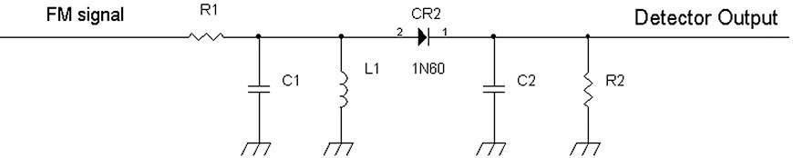
FIGURE 11-30 A band-pass filter that is “off-tuned” from the center of the IF.
If two band-pass filters are used instead and tune above and below the IF, a more linear or lower distortion FM slope detector can be made (see Figure 11-31). By implementing two half-wave rectifiers as shown in Figure 11-32, a differential slope detector is provided.

FIGURE 11-31 Frequency responses of two separate band-pass filters tuned to above and below the center frequency, with the vertical axis denoting amplitude and the horizontal axis showing frequency.
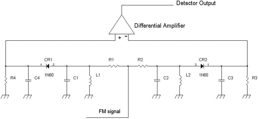
FIGURE 11-32 One implementation of a differential slope FM detector.
As shown in Figure 11-32, resonant circuits L1/C1 and L2/C2 are tuned to below and above the center IF of 10.7 MHz (e.g., 10.5 MHz and 10.9 MHz). The spread of the bandwidth of each filter is set by resistors R1 and R2, which determine the Q factor of the two parallel LC tank circuits.
Note that the slope detection with the L1/C1 that is tuned below 10.7 MHz converts the changes in frequency due to the FM signal to create an AM signal that is rectified for the positive cycle of the created AM signal. Likewise, the slope detection for L2/C2 is at frequencies above 10.7 MHz with rectification on the positive cycle. A differential amplifier takes the two demodulated AM signals and provides a subtractive process. The resulting FM detection curve is shown in Figure 11-33.
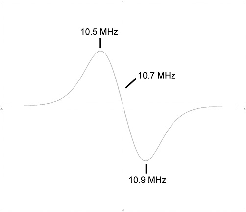
FIGURE 11-33 By subtracting the two peaks as shown in part a, an inverted or upside-down S detection curve is achieved.
The resulting detection transfer function curve shows a wider frequency-detection range with a straighter line for demodulation of the FM signal as the frequency of the IF deviates below and above the center frequency. Also, at the resting frequency, 10.7 MHz, the detector’s output is zero, which may be useful in driving a center tune meter.
Differential peak detector chips were implemented as the CA3075 and CA3065 ICs (integrated circuits) for FM radio and FM TV sound. In those circuits, a combination band-reject and low-pass filter was used in place of the two LC tank circuits (see Figure 11-34). The circuit shown in Figure 11-34 works on the principle that a single inductor L1 and two capacitors C1 and C2 form two resonant frequencies to mimic two separate band-pass filters. Again, this circuit is a form of differential slope detection. It relies on two slopes, a positive- and negative-going slope when the frequency response is swept from below the IF to above the IF.
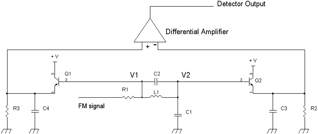
FIGURE 11-34 Using a low-pass filter to form a differential peak FM detector.
From the RCA CA3075 data sheet, typical values for the R1, L1, C1, and C2 are 2.7 kΩ, 5.5 μH (preferably an adjustable inductor), 6.8 pF, and 33 pF, respectively. The detection range can be modified by adding a 33 kΩ resistor in parallel with L1.
R1, L1, C2, and C1 form two types of filters. At node V1, which goes to the base of Q1, there is a notch or band-reject filter effect. At node V2, this is the output of a two-pole low-pass filter with a “transmission zero” or notch frequency formed by L1 and C2. At V1 and V2, there are two notch frequencies, and the notch frequency at V1 is lower than the one at V2. In principle, the frequency response curves of V1 and V2 will intersect or cross each other. That is, from 10.6 MHz to 10.8 MHz, the frequency response at V1 shows an upward slope due to the band-reject response coming back up after the notch frequency, whereas the frequency response at V2 shows a downward slope due to the low-pass filtering effect.
Transistor peak detectors Q1 and Q2 provide the same half-wave rectification as diodes except that they provide high-impedance inputs at their bases so as not to load the filter circuit (R1, L1, C1, and C2) down. The emitters of Q1 and Q2 are then connected to peak-hold capacitors C3 and C4 with their current discharge rate controlled by R2 and R3. A differential amplifier then takes the difference voltages from C4 and C3 to provide a demodulated FM signal at its output.
In practice, this circuit is rather tricky to implement because capacitor C1 is only 6.8 pF, and any parasitic capacitances from the board layout or input of the transistors must be taken into account. Also, the separation between the two notch frequencies may be excessive, and their frequency-response curves may not “exactly” intersect at the center frequency of 10.7 MHz. If the notch frequencies are too far apart, (only) one slope (either at V1 or V2) will be taken advantage of rather than both slopes (at V1 and V2) for FM detection.
And now we turn to the original differential slope detection, which is known as the stagger-tuned detector. This circuit preceded the ratio detector, the Foster Seeley FM discriminator, and the differential peak detector that used a differential amplifier. Instead of having to provide a differential voltage V1–V2, it merely inverted one of the voltages and stacked or added the two voltages in series. Let’s see how that works (see Figure 11-35).
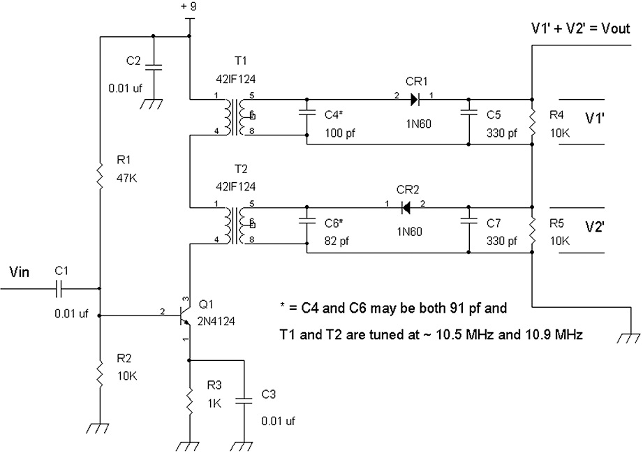
FIGURE 11-35 Stagger-tuned FM detector.
The stagger-tuned circuit shown in Figure 11-35 uses two 10.7 MHz IF transformers T1 and T2. The 42IF124 transformers do not have the internal capacitors, and the external resonating capacitors C4 and C6 are shown for clarity so as to indicate that two resonating frequencies are involved. T1 is tuned to slightly below the center IF of 10.7 MHz, such as 10.5 MHz, to provide slope detection of the FM signal, which results in a “transformed” AM signal across C4. This AM signal is rectified via CR1 for the positive peaks of the transformed AM signal, and the demodulated signal is provided across C5 and R4 for a detected voltage V1’.
Resistor R4 also plays a role in determining the Q factor of the tank circuit via the secondary inductance of T1, which is nominally 2.4 μH. Higher or lower Q is possible by increasing or decreasing the value of R4 to determine the steepness of the slope detection. However, both R4 and R5 should be the same value for best detection linearity or lowest distortion for the demodulated FM signal.
Likewise, T2 is set to resonate above the center IF at about 10.9 MHz. The voltage across C6 is another “transformed” AM signal, which is rectified by CR2 for the negative cycles instead of the positive cycles. By rectifying negative cycles, the detection curve is mirror-image flipped upside down to provide a detected voltage V2’. Also, R5 plays the same role of affecting Q, but for T2.
The combined series voltages V1’ + V2’ form an FM detection curve similar to the one shown in Figure 11-33 because V2’ is a negative voltage. When the IF FM signal is sitting at rest or at 10.7 MHz, Vout = 0 volts. As the IF signal swings below 10.7 MHz, there is a positive voltage, and when the IF signal swings above 10.7 MHz, there is a negative voltage.
To tune for T2 at approximately 10.9 MHz, connect an RF generator at 10.9 MHz to the Vin terminal. Set the generator’s amplitude level to about 100 mV peak to peak. Monitor the DC voltage at the anode of CR2, and adjust the slug in T2 for maximum negative voltage. To tune for T1, first temporarily short the anode of CR2 to ground. Set the generator for 10.5 MHz, and measure the DC voltage at the cathode of CR1. Adjust T1’s tuning slug for maximum DC voltage. Remove the short circuit from the anode of CR2 to ground.
Vout preferably should be buffered with an amplifier to ensure that the Q values of the two LC tank circuits are not affected by loading downstream. Also notice that the primary windings are connected in series. This is done so that there is truly independent tuning for T1 and T2. Recall that a current source that drives two circuits in series “forces” the signal current equally into the two circuits. If the primary windings of T1 and T2 were connected in parallel, then tuning T1 would affect the tuning of T2, and vice versa.
References
1. Ronald Quan, Build Your Own Transistor Radios. New York: McGraw-Hill, 2013.
2. K. Blair Benson and Jerry Whitaker, Television Engineering Handbook. New York: McGraw-Hill, 1992.
3. “RCA Linear Integrated Circuits and MOS/FET’s,” RCA Solid State, Somerville, NJ, 1982.
4. Robert L. Shrader, Electronic Communication, 2nd ed. New York: McGraw-Hill, 1967.
5. Robert G. Meyer, “EE140 Class Notes on Nonlinear Electronic Device Models and Circuits,” University of California, Berkeley, CA, 1975.
6. Robert G. Meyer, “EE240 Class Notes on Nonlinear Analog Integrated Circuits,” University of California, Berkeley, CA, 1976.
7. Kenneth K. Clarke and Donald T. Hess, Communication Circuits: Analysis and Design. Reading, MA: Addison-Wesley, 1971.
8. A. Bruce Carlson, Communication Systems: An Introduction to Signals and Noise in Electrical Communication, 3rd ed. New York: McGraw-Hill, 1986.