
CHAPTER 13
![]()
Video Circuits and Systems
Video signals are a little bit more complicated than audio signals because they have to include synchronizing information (e.g., sync pulses, color burst signals, etc.). Horizontal and vertical synchronizing signals are essential to command a display when and where to display the picture information. Also, unlike audio signals that can be additively mixed together with any other audio signal, video signals have to synchronize in phase and frequency to each other or to a common clock signal before any additive mixing can be done.
This chapter will show how to control the contrast, brightness, sharpness, and horizontal picture position for a display. The circuits that implement these functions on their own belong to a video processing system that includes extra circuitry to ensure that timing (e.g., sync signals) and black or blanking levels are set properly. A four-page schematic of a video processor is provided, which requires advanced hobbyist skills and is not meant to be an actual project. However, if the reader is up to building such a circuit, by all means please try. In addition to showing how to make a practical video processor that allows adjustment for contrast, brightness, and sharpness of an external TV signal, we will illustrate how to make a video scrambler.
How Easy Is It to Make a Brightness and Contrast Video Circuit?
If the video signal is internal to a display such as a TV monitor where the vertical and horizontal sync signals have already been extracted and used within the TV monitor, then the brightness and contrast circuits include just a direct-current (DC) offset and an adjustable-gain amplifier. However, when brightness and contrast controls are implemented for video signals outside the TV set, the circuitry is a bit more complicated.
Let’s start with the brightness control, where we want to add brightness adjustment from an external video signal such as one from a DVD player. If a DC offset voltage is simply added to the video signal and sent to a TV set as seen in Figure 13-1, then there will be no effect.
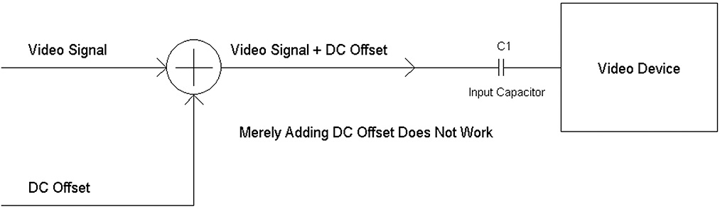
FIGURE 13-1 A DC offset voltage is added to the input video signal.
As seen in Figure 13-1, most video devices such as a TV set have an AC (alternating-current) coupling capacitor (e.g., C1) that blocks any DC offset voltage. Thus there will be no change in brightness with the DC offset voltage added.
To add a brightness signal, the DC offset voltage is added selectively to the active video line portion of the video signal. This active video line portion in a standard-definition TV signal is about 52 μsec (μsec = microsecond = μs) in length and starts about 10 μsec after the start of the horizontal sync pulses (see Figures 13-2 and 13-3). In Figure 13-2, a switch allows passage of the DC offset voltage during active video line only to add a pedestal voltage to the video signal’s pixel voltage. The active line gate signal is generated from a sync separator circuit along with a timing generator. Figures 13-4 and 13-5 provide examples of increasing and decreasing the brightness of a video signal.
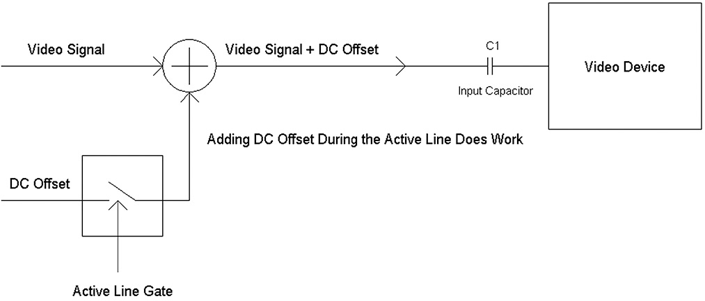
FIGURE 13-2 Controlling brightness to a video signal is accomplished by selectively adding the DC offset voltage.

FIGURE 13-3 Convergence pattern of a test signal with 0 volt DC offset voltage added to the active line portion of the video signal.
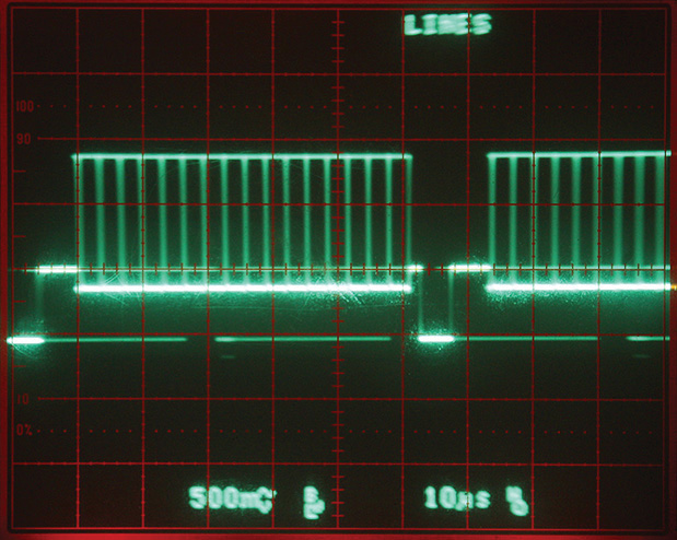
FIGURE 13-4 An example of adding a negative DC offset voltage during an active line portion to decrease the brightness of a video signal.
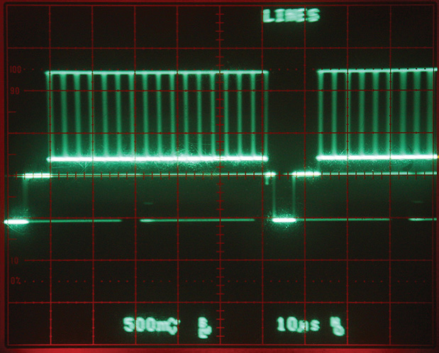
FIGURE 13-5 An example of adding a positive DC offset voltage to increase brightness.
We now turn to adjusting the contrast of a video signal. In a TV set, this is done by simply changing the amplitude of the video signal. However, if we do this when an external input video signal is provided, as shown in Figure 13-6, we encounter a problem.
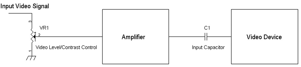
FIGURE 13-6 Varying the amplitude of a video signal.
In Figure 13-6, when the video signal level is varied, both the pixel information’s amplitude and the synchronizing pulses’ level will be changed. If VR1 is adjusted for low amplitude to provide a low-contrast picture, the horizontal and vertical synchronizing pulses will be attenuated to cause the TV set to unlock. To ensure that the TV set will always lock, a solution is to vary the pixel amplitude but keep the sync pulses at their normal amplitude (see Figure 13-7).

FIGURE 13-7 Inserting “New Sync” to ensure that a stable picture is viewed while varying the contrast.
When we look at Figure 13-7, we see something that is more of a system than a simple circuit. There is a timing generator, a clamped black level amplifier, a (regenerated) sync generator (“New Sync”), and a multiplexer. All these circuits are necessary to provide changes in video levels while not affecting the amplitude of the sync timing pulses.
The timing generator consists of a sync separator that literally extracts the horizontal and vertical synchronizing pulses from the input video signal. Once the synchronizing pulses have been extracted, they can be inserted into a new video signal that contains the active video signal whose amplitude is adjusted. The timing generator also sends a control signal (sync gating pulse) to the multiplexer such that regenerated sync pulses are inserted appropriately with the varied amplitude video signal.
A black level clamp circuit is required to establish the blanking level correctly. Many video signals are AC coupled, and with different scenes such as dark and bright ones, the blanking level will vary (see Figures 13-8 through 13-10).
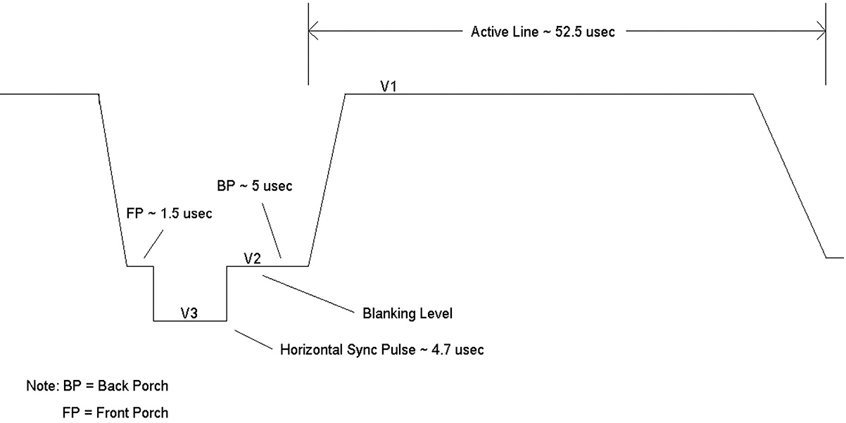
FIGURE 13-8 A video signal with identification of the front porch, horizontal sync pulse, and back porch.
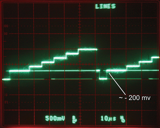
FIGURE 13-9 An AC-coupled video signal with a stair-step signal.
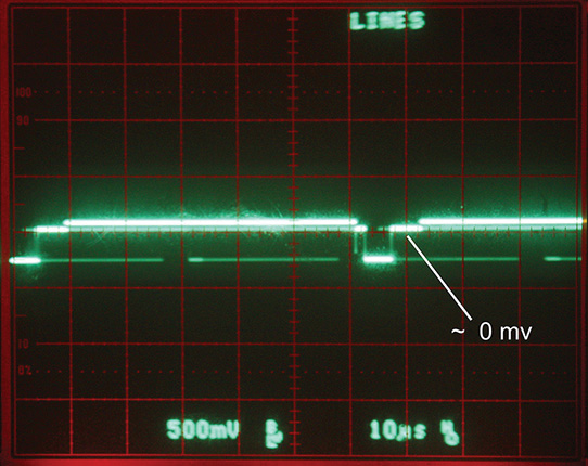
FIGURE 13-10 An AC-coupled video signal that is representative of a black level.
As shown in Figure 13-8, there are four basic components to a TV line. The beginning of the “front porch” region denotes the end of the active line portion of the previous line and thus is the start of the next TV line. Its voltage level is the blanking voltage V2, which is called the blanking level. The blanking level is generally the black level, except in the case of NTSC, where black is 7.5 percent of the white level (7.5 IRE units, where IRE = Institute of Radio Engineers, and the peak white level is at 100 IRE units), and the blanking level is 0 percent (0 IRE units), which is lower than the (NTSC) black level.
The sync tip level is at V3, and the sync pulse amplitude is (V2 – V3). The normal sync amplitude is 286 mV peak to peak for NTSC and 300 mV for PAL.
NOTE The number 286 is not exactly easy to remember, but if you are into vintage computers, think of the 286 processor, which was succeeded by the 386, and later by the 486 central processing units (CPUs).
The “back porch” region is normally set at the blanking level, and this region is commonly sampled by clamp circuits to set the blanking level or back porch voltage to a predetermined level. Following the back porch, the pixel information is located at the active line portion and its level is denoted by V1 and its amplitude is (V1 – V2). For NTSC, the pixel voltage value for a standard-level signal (V1 – V2) is between 0 mV and 714 mV and for a PAL signal (V1 – V2) is between 0 mV and 700 mV. Peak white is then 714 mV in the NTSC TV standard.
NOTE 714—where did this number come from? “Dum dee dum dum.” The 714-mV number is a result of the fact that from peak white to sync tip, the voltage is (V1 – V3) = 1,000 mV, or 714 = (1,000 – 286). Or another way I have told people how to remember 714 is to think of Sgt. Joe Friday’s badge number, 714, on the TV show Dragnet. After all, this is a chapter on TV.
Now we turn to the effects of AC coupling a video signal and how the back porch signal’s voltage level changes with different video signals. Note in the AC-coupled stair-step signal in Figure 13-9 that the back porch level is a negative voltage that is below 0 volts at about –200 mV. The stair-step signal has an average picture level of about 50 percent.
Notice that the black-level signal in Figure 13-10, when AC coupled, has its back porch level close to 0 volts, and its average picture level is about 0 percent. The clamped black-level amplifier in Figure 13-7 can receive an AC-coupled video signal and then restore the black level (e.g., back porch level) to a predetermined voltage such as 0 volts regardless of the average picture level of the input video signal (e.g., when the video signal = 0 percent white or 100 percent white). We will later show a method to keep the back porch level set to a predetermined voltage via a feedback clamp circuit.
A Sharpness Circuit: Can It Be Simple?
It turns out that to make a stand-alone sharpness circuit, a sync separator and timing circuits are not necessary. Since the sharpness circuit affects the high-frequency response of the video signal, it can be treated like an audio equalizer for a stereo system (see Figure 13-11).
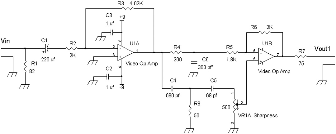
FIGURE 13-11 A practical phase linear sharpness control with the “Batman’s ears” pulse response.
The sharpness circuit in Figure 13-11 is similar to the one in Figure 12-19 except that there is an analog signal delay circuit formed by R4 and C6. This delay circuit is necessary because high-pass filters C4, R8, C5, and VR1A produce a slight time delay. Even though the high-pass filters provide the double-pointed peaks when a pulse signal is present in Vin, these peaks are delayed somewhat, and when combined via the (+) input of U1B with the output signal from U1A, one of the peaks gets hidden in the rising or falling edge of the pulse signal, leaving only the overshoots visible without preshoots.
Low-pass filter and delay circuit R4 and C6 then provides the proper delay of the pulse signal such that the pulse response has both peaks (preshoot and overshoot) at the output of U1B (for a pulsed waveform). Figures 13-12 to 13-15 show various frequency responses of a multiburst signal for different sharpness settings and a pulse response at the maximum sharpness setting.

FIGURE 13-12 Sharpness control set for flat frequency response.
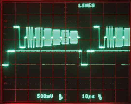
FIGURE 13-13 Sharpness control set to roll off the frequency response for a softer-looking picture.
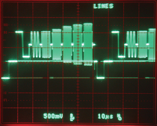
FIGURE 13-14 Sharpness control set to enhance the high-frequency response to provide edge enhancement.
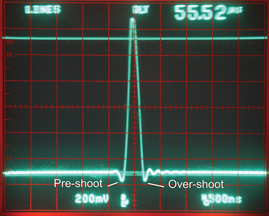
FIGURE 13-15 Pulse response when sharpness control is set at maximum provides preshoot and overshoot pulses.
NOTE It was found for the ciruit in Figure 13-11 that C6 can be in the range of 270 pF to 330 pF.
A Video Processor to Adjust for Brightness, Contrast, and Sharpness
We will now show a video processor circuit, which requires a DVD player with the Y-channel output of the component or S-video connection connected to the video processor. The DVD player is set to standard-definition TV (SDTV), either 480i (derived from the NTSC 525-line TV standard) or 576i (derived from the PAL 625-line TV standard). A TV monitor or display will also be needed to see the adjustment effects of the video processor. Also, it is highly recommended that a two-channel oscilloscope of at least 15-MHz analog bandwidth is used in observing the various video and timing waveforms from the video processor.
This video processor circuit may be more advanced and complicated than any of the previous circuits shown so far because it is a combination of many different circuits. Figure 13-16 shows a top-level block diagram.

FIGURE 13-16 Block diagram of the video processor.
An input video signal source is connected to Vin, which is connected to two circuits, a sync separator and the input to the contrast-sharpness circuit. With the video signal coupled to the contrast and sharpness circuit, a video signal-amplitude control via a potentiometer allows adjustment of the contrast. Another control allows adding high-frequency signals derived from the video signal to add edge enhancement and high-frequency equalization to the video signal. The output circuit for the contrast and sharpness control also has a blanking level clamp circuit that allows the blanking level to be varied from a negative voltage to a positive voltage. Normally, the voltage blanking level is set to “about” 0 volt.
A processed video signal is provided at the output of the contrast and sharpness circuit. This circuit also has a variable or controllable blanking voltage that will later allow for changing the brightness. This processed video signal is fed to one of the two inputs of the multiplexer circuit.
NOTE The blanking level is generally the black level of a video signal. In “older” 525-line TV standard sets used in the United States, blanking level = 0 percent of peak white level, whereas the black level = 7.5 percent of the peak white level. However, in most other TV standards, the blanking level = black level, which is 0 percent of the peak white level.
As previously mentioned, to change the contrast of a video signal requires more circuitry to ensure that the horizontal and vertical synchronizing signals are not affected when the contrast control changes the amplitude of the pixel information. At some point, we need to insert new sync pulses that are not affected by controlling the contrast. This requires a sync separator to extract the synchronizing signals from the input video source. The output of the sync separator circuit provides a “derived” sync signal, which is fed to timing circuits that allow “New Sync” signals to be inserted with the processed video signal.
Another job of the timing circuits is to provide a multiplexer control signal that commands the multiplexer to insert the new synchronizing, front porch, and back porch signals into the processed video signal. Finally, the timing circuit also provides a sampling pulse that is coincident within the back porch region of the input video signal. This back porch pulse serves as the clamp pulse for the contrast and sharpness output amplifier.
The video processor can be used to alter the brightness, contrast, and sharpness of a DVD program, as shown in Figure 13-17. Most DVD and Blu-ray players include a Y (luma) output signal connector, which can be used as the video source for the video processor to vary the contrast, brightness, or sharpness of the displayed picture (see Figure 13-18). The video processor circuits shown in Figures 13-19 through 13-22 will require a standard-definition Y (black and white) interlaced TV signal. Either 480i or 576i will do.
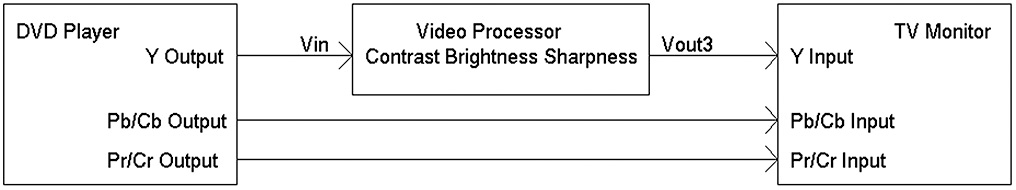
FIGURE 13-17 Video processor integrated with an example DVD player and TV monitor.
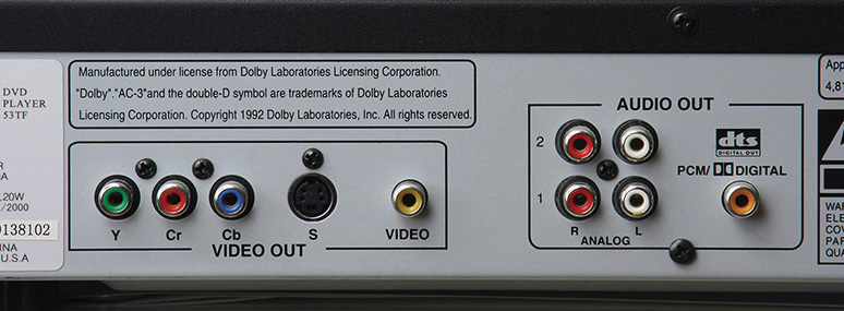
FIGURE 13-18 The Y, Pr (Cr), and Pb (Cb) video outputs with RCA connectors on the back of a DVD player.

FIGURE 13-19 Schematic diagram for adjusting contrast, brightness, and sharpness.
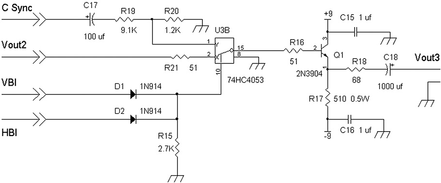
FIGURE 13-20 Output circuit with sync replacement.

FIGURE 13-21 Input circuit with sync separator circuit.

FIGURE 13-22 Timing circuits to provide horizontal blanking interval and composite sync signals.
Now let’s look into the circuits, which are divided among four pages. We start with the contrast, brightness, and sharpness circuits that include a feedback clamp circuit.
Parts List
• C1, 220 μF 16 volts
• C2, C3, C9, C11, C12, C13, C14, C15, C16, C20, C21, C23, C27, C29, C33, C37, and C38, 1 μF film or ceramic 5% or 10%
• C4, 680 pF, 5% or 10% silver mica or ceramic
• C5, 68 pF 5% or 10% silver mica or ceramic
• C6, 300 pF or alternatively, 330 pF or 270 pF) 5% silver mica or ceramic
• C7, C8, 0.1 μF, 5% film
• C10, C17, C19, and C34, 100 μF 16 volts
• C18, 1000 μF 16 volts
• C22, 10 μF 25 volts
• C24, C26, C31, C32, C35, and C36, 0.001 μF, 5% film
• C25, 82 pF (or, alternatively, 100 pF) 5% or 10% silver mica or ceramic
• C28, 0.01 μF, 5% film
• C30, 330 pF, 5% or 10% silver mica or ceramic
• D1, D2 1N914, or 1N4148 silicon diodes
• Q1, Q2, Q3, and Q4 2N3904 or 2N4124 NPN transistors
• DIP 8 socket for U1 (socket is for experimenting with other op amps)
• U1, LM49720 (LM4562) or LM6172 eight-pin DIP dual op amp
• U2, TL082, LF353, or TL072 eight-pin DIP dual op amp
• U3, 74HC4053 or 74HCT4053 triple analog switch
• U5,74HC14 CMOS Schmitt trigger hex inverter
• U6, U8, and U9, 74HC221 dual one-shot monostable
• U7,74HC74 or 74HCT74 dual D flip-flop
• U10,74HC00 or 74HCT00 quad NAND gate
• +9 volt and –9 volt supply from batteries or a regulated ±9 volt to ±12 volt supply
• All resistors are ¼ watt, 5% unless noted
• R1, 390 Ω
• R2 and R7, 2 kΩ
• R3, 6.2 kΩ
• R4, 200 Ω
• R5, 1.8 kΩ
• R6, 6.8 kΩ
• R8, 51 Ω
• R9, R10, 2.21 kΩ 1%
• R11 and R28, 100 kΩ
• R12, 47 Ω
• R13, R14, R22, R30, R32, R35, and R40, 10 kΩ 1 percent (Note: R40 may be 10 kΩ 5%)
• R15, R23, R24, and R31, 2.7 kΩ
• R16 and R21, 47 Ω or 51 Ω
• R17, 510-Ω, ½ watt, 5% or alternatively, parallel two 1kΩ resistors for R17
• R18, 68 Ω
• R19, 9.1 kΩ
• R20, 1.2 kΩ
• R25 and R26, 1 kΩ
• R27, 220 Ω
• R29, 4.7 kΩ
• R33, 3.32 kΩ, 1%
• R34, 100 kΩ, 1%
• R36, 49.9 kΩ, 1%
• R37, 1 kΩ, 1%
• R38, 1.5 kΩ
• Potentiometers are ⅛ watt to ¼ watt rating
• VR1A, 500 Ω pot
• VR2A, 100 Ω pot
• VR3, 50 kΩ pot
• VR4, 5 kΩ pot
The video signal from a DVD player’s Y channel is connected to Vin, which is coupled to a variable voltage divider circuit formed by VR2A (Figure 13-19). The output of VR2A is AC coupled to an inverting-gain amplifier U1A that has a fixed gain of approximately –3. Typically, Vin with a peak white signal will be on the order of 1 volt peak to peak since R1 in parallel with VR2A forms approximately 75 Ω for the standard input resistance. By adjusting VR2A, the output of U1A at pin 1 varies between 0 volts and 3 volts peak to peak of an inverted video signal.
To turn the video signal back into its noninverting form, U1B forms a unity-gain inverting amplifier via feedback resistor R7 and series input resistors to pin 6 of R4 and R5. The voltage gain from pin 1 to pin 7 of U1A and U1B is
–[R7/(R4 + R5)] = [2,000/(200 + 1,800)] = –1
To provide a range of high-frequency boost to the video signal that results in edge enhancement and an improvement in resolution, two high-pass filter sections C4, R8, C5, and VR1A add a high-frequency signal into pin 5, the (+) input terminal of U1B. The high-frequency signal’s amplitude is adjustable via potentiometer VR1A. At the output of pin 7 of U1B is a video signal that has variable amplitude and sharpness via VR2A and VR1A, respectively.
We now also want to establish a predetermined or adjustable blanking level of the output signal at pin 7 of U1B. To accomplish this, a sample and hold circuit via U3C and C7 “records” the voltage of the video signal at pin 7 of U1B during a portion of the back porch period (approximately 3 μsec out of the approximately 5 μsec back porch period), which is after the trailing edge of sync pulses. Variable resistor VR3 allows adjustment of a range of positive to negative voltages via the +5v and the –5v voltage sources connected to R9 and R10. U2B serves as a feedback integrating amplifier with C8 and send a clamp error signal to R6.
The DC voltage at the slider of VR3 servos or forces the back porch voltage of the video signal to be the same voltage. For example, if the voltage is 0 volt at the slider of VR3, pin 7 at U1B will have a video signal whose back porch voltage is 0 volt. If the voltage at the slider of VR3 is +150 mV DC, then the video signal at pin 7 will have DC offset, and its back porch voltage will be +150 mV. Likewise, if VR3 slider’s voltage is –100 mV DC, the resulting video signal at pin 7 will have a negative DC offset with its back porch voltage at –100 mV.
To provide a regulated +5 volt source to R9, U4, a low-power TO-92 positive regulator (78L05) integrated circuit (IC), is connected to the raw power supply of +9 volts. This regulated +5 volt source is also used to power the logic gates, analog switches, one-shot timing circuits, and sync separator circuit R28, Q4, and R29.
A regulated –5 volts is generated by using an inverting-gain op amp circuit U2A with resistors R13 and R14. The output at pin 1 of U2A is connected to a 47 Ω resistor prior to connection to capacitor C10 to avoid oscillation. An op amp in general does not load well directly into a capacitor and requires a small-value series resistance (e.g., 47 Ω) to isolate its output terminal from a capacitive load. The analog switch U3 requires a negative voltage because there will be a positive and a negative voltage range video signal at the input of one of the analog switches.
NOTE Although an LME49720 (or, equivalently, an LM4562) audio op amp is used for this video-processing circuit, it is well advised that the circuit be made with an 8 pin DIP socket. The socket allows easier changing of op amps. Higher-performance op amps suitable especially for video purposes such as the LM6172 and AD828ANZ can be used instead.
The output of U1B is Vout2, which is connected to the X input (pin 2 via R21) of the 74HC4053 analog switch (see Figure 13-20). The C Sync signal is a logic-level signal from 0 to +5 volts. Capacitor C17 blocks the DC voltage and level shifts the signal to be approximately 0 to –5 volts at R19. By dividing the C Sync signal appropriately via R20 and R19, a “New Sync” signal from about 0 to –600 mV is provided to the Y input terminal of U3B. When the command or control signal at pin 10 is logic high, the “New Sync” signal at pin 1 of U3B is transferred to the output of the switch at pin 15 of U3B and to R16.
The command signal to insert or switch in the “New Sync” is a combination of two sources, the VBI (vertical blanking interval) and the HBI (horizontal blanking interval) signals. These two signals, VBI and HBI, are logically OR’d via diodes D1, D2, and R15.
When the VBI command is logic high, vertical sync signals from the original video input source are inserted. For inserting new horizontal sync signals, the HBI signal enables a high-logic level pulse to gate in the new front porch, sync pulse, and back porch signals. Also, as we will see later, the horizontal sync pulse is variable in phase or time-wise to demonstrate centering the displayed picture in a lateral manner.
Output amplifier emitter-follower Q1 buffers (amplifies with an approximate gain of 1) the processed signal that has adjustable contrast, brightness, and sharpness along with “New Sync” to the output terminal Vout3 via DC blocking capacitor C17. When Vout3 is terminated with 75 Ω, the sync level is reduced to half to provide about 300 mV peak to peak, which is a standard sync amplitude level. Note that R17, a 510 Ω, ½ watt resistor may be substituted with two 1 kΩ, ¼ watt resistors connected in parallel. Now let’s look at Figure 13-21 (sync separator).
To extract the sync pulses from the input video signal (e.g., Y channel output from a DVD player or TV tuner), the input signal is amplified by about –2.7 × via common-emitter amplifier Q2 with collector load resistor R24 and emitter resistor R25. The gain is set by approximately –R24/R25 = –2.7 kΩ/1 kΩ = –2.7.
An inverting video signal with its positive-going sync pulses at about 2.7 × 0.3 volt = 0.8 volt is provided at the collector of Q2. Emitter follower Q3 provides a low-impedance drive signal into the sync separator circuit C22, Q4, R28, and R29. From the negative end of C22, the inverted video signal has positive-going sync pulses DC restored to about 0.7 volt at the sync tips. The base-emitter junction of Q4 acts like a diode with the anode connected to the – terminal of C22 and the cathode connected to ground. R28 is biased to + 5 volts to DC restore the sync tips to +0.7 volts and turn on Q4 as a switch. When the inverted sync pulse (from the inverted video signal at Q2’s collector) drops below +0.7 volt, Q4 turns off. As a result, a negative-going sync pulse from about 0 volt to +5 volts is provided at the collector of Q4. Any video information or voltage levels, which are at least 0.8 volt below (inverted) sync tip at the base of Q4, are ignored.
Inverter gate U5A then inverts the sync-separated pulses to positive-going pulses. These positive-going sync pulses are sent to the data or D input of a flip-flop circuit U7A. A delayed version (approximately 0.2 μs delay) of these positive-going pulses via U5B, R31, C25, and U5C is coupled to the positive trigger input of one-shot multivibrator U6B. The output of U6B at pin 12 provides a negative-going approximately 3 μs pulse that is framed within a normal 4.7 μs wide horizontal sync pulse.
Whereas an analog switch and capacitor form a sample-and-hold circuit for an infinite number of levels in an analog signal, a D flip-flop is like a 1-bit sample-and-hold circuit. Both circuits will latch onto the value of the input signal during the sample pulse. In the analog switch U3C in Figure 13-19, the video signal provides the voltage to be sampled by the clamp pulse.
In a D flip-flop, the input is at the D input terminal, pin 2 in this case, and the sampling pulse is the output of the one-shot timing circuit at pin 12 of U6B. The 74HC74 samples the D input during the rising edge of the clock pulse at pin 3 of U7A.
So let’s see why a flip-flop is being used to sense a beginning of the vertical blanking interval or, put another way, at the end of the active field. When an active field ends in the TV signal, there are pre- and post-equalizing sync pulses that precede and follow the broad vertical sync pulses. These equalizing pulses are half the width (2.3 μsec) of the 4.7 μsec wide horizontal sync pulses.
The object, then, is to detect the first pre-equalizing pulse and generate a VBI signal. When horizontal sync pulses of 4.7 μsec are at the D input, U7A will output a logic-high output signal at pin 5 because the clock pulse triggers a rising edge at 3 μsec away from the leading edge of horizontal and all sync pulses and catches a high state of the positive-going horizontal sync pulse.
However, when a 2.3 μsec pre-equalizing pulse is inputted into the flip flop, the 3 μsec clock pulse will go past the high state of this pre-equalizing pulse and catch a low state instead. The output at pin 5 of U7A then goes from logic high to logic low when the first pre-equalizing pulse is sensed. The complementary output of U7A is pin 6, which goes high at detection of the first pre-equalizing pulse, and this positive-going pulse triggers one-shot timing circuit U6A to generate a pulse of approximately 100 kΩ × 0.01 μF = 1 msec (msec = millisecond) to provide the VBI pulse at pin 13 (at U6A).
For illustration purposes, Figure 13-21 also shows the traditional method of sensing vertical sync pulses that are approximately 27 μsec wide versus the 4.7 μsec pulsewidth of a horizontal sync pulse. This method includes a simple RC low-pass filter R30 and C24 that filters the horizontal and vertical sync pulses. Negative-going sync pulses are fed to R30, and when the low-state vertical sync pulses are present, the voltage across C24 will drop sufficiently to allow inverter gate U5E at pin 10 to flip to a positive-going vertical pulse with a frequency of about 60 Hz or 59.94 Hz. Although the signal at pin 10 of U5E is not used for other parts of the video processor, it can be used as a vertical rate-triggering pulse signal for an oscilloscope.
We will now explain how the back porch sampling pulse (BPSP) is provided by U5D pin 8. The slightly delayed positive-going sync pulses from U5C pin 6 are coupled to a high-pass filter C30 and R32 to generate a negative going spike on the falling edge of the positive-going sync pulses. This negative spike is on the trailing edge of the sync pulse and starts in the beginning of the back porch area of the video signal. U5D also serves as a half-shot timing generator, which provides a positive-going pulse of approximately 3 μs within the approximately 5 μs-wide back porch of the video signal. This pulse then is used for sampling the back porch or blanking-level voltage of the incoming video signal for U3C in Figure 13-19.
For generating the HBI (horizontal blanking interval) signal, which is a pulse about 11 μs long, we start with a negative-going composite sync signal from pin 4 of U5B (Figure 13-22). First, we trigger the leading edge of sync via U8B to generate about a 10 μs pulse via pin 5 that ends at the beginning of the active video line. The output pulse at pin 5 of U8B is then sent to the negative or falling edge trigger input of the next timing generator U8A, which generates a pulse at pin 13 indicative of the active video line, about 52 μsec. The inverted output at pin 4 of U8A then is low during the active horizontal line portion of the video signal and high during the horizontal blanking interval (HBI) that includes the front porch, horizontal sync pulse, and back porch areas.
To regenerate the vertical and horizontal sync pulses, we could just insert sync pulses from pin 4 of U5B for the C-Sync signal and be done and go home. However, wouldn’t we like a little adventure? Why not show the effects of phasing the picture laterally and add wiggle as well? That is, we can shift the picture on the display from side to side manually with a potentiometer or, alternatively, couple a signal generator or audio signal source to U8A to electronically shake the picture up to provide scrambling.
Nominally, the output pulse at pin 13 of U8A finishes at the end of the active TV line. At this point, U9B provides about a 1.5 μsec pulse to start the newly regenerated horizontal sync pulse of 1.5 μsec (the duration of the front porch) into the horizontal blanking interval. U9A generates horizontal sync pulses of the standard 4.7 μsec pulsewidth via pin 13 of U9A. These regenerated horizontal pulses can be shifted to lead or to lag, which causes the TV monitor to display the picture to the side in either direction or centered correctly via H Phase variable resistor VR4.
If a sine wave or any other waveform of frequency less than 15 kHz is inputted to C34, the regenerated horizontal sync pulses will be position modulated that results in a wiggle. Typical amplitudes would be on the order of 200 mV to 1.2 volts peak to peak depending on the strength of the horizontal shift. The modulated waveform’s amplitude is attenuated approximately tenfold via R40 and R37. By modulating the voltage at VR4 and R36, the charging time of C32 is varied to provide a pulsewidth-modulated signal from pin 13 of U8A.
To insert regular vertical sync pulses and the regenerated horizontal sync pulses, we multiplex or switch between the types of sync pulses to provide the regenerated composite sync signal, C Sync. By using the VBI (vertical blanking interval) signal, the derived vertical sync pulses from the input video signal is spliced in with the regenerated horizontal sync pulses that are capable of position modulation.
When the VBI signal is logic high, the vertical sync signals from the sync separator are switched to the output of the multiplexer, U10A pin 3. The regenerated horizontal sync signals that can be position modulated are switched to pin 3 of U10A when the VBI signal is logic low, which happens during the active video field. The vertical and horizontal sync signals are then sent to the (+) terminal of C17 (Figure 13-20), which couples these sync signals to U3B for insertion into the processed video signal that allows adjustment for contrast, brightness, and sharpness.
To experiment with modulating the phase or position of the new horizontal sync pulses, a function generator is connected to C34 (negative side) and ground in Figure 13-22. Frequencies from 100 Hz to 100 kHz can be tried. The sensitivity of the positional shift is that about 1.2 volts peak to peak from the (function) generator results in about 2.3 μsec peak to peak of horizontal sync displacement. At frequencies near the horizontal line frequency, fH (e.g., approximately 15.734 kHz for 480i and approximately 15.625 kHz for 576i), the scrambling effect has approximately a frequency = |fH – fosc|, where fosc is the oscillator frequency. One will find that when the oscillator is set close to multiples of fH, there will also be picture-displacement effects. For a reference, Figure 13-23a has no modulation.
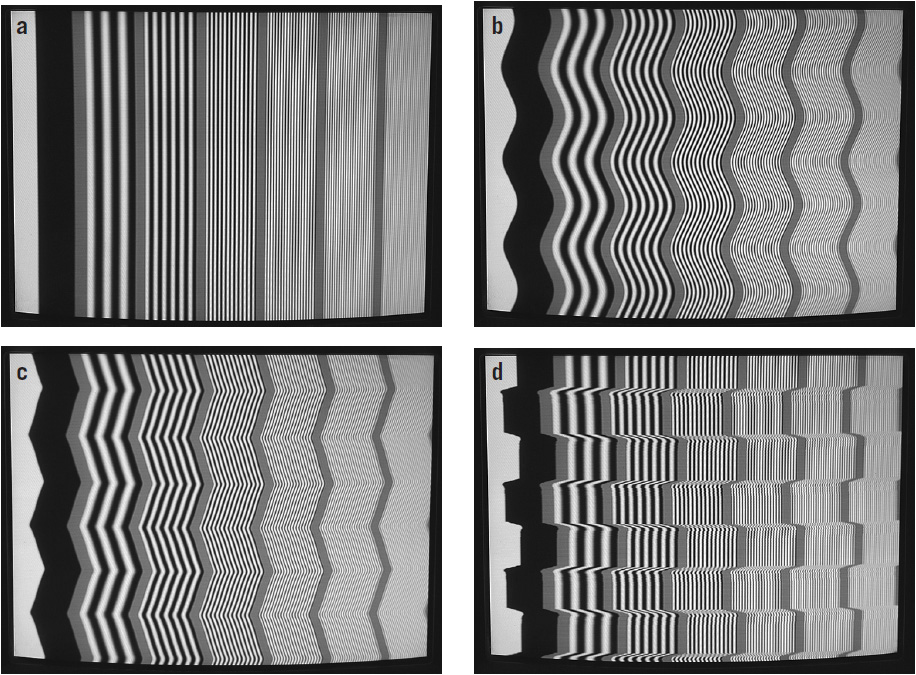
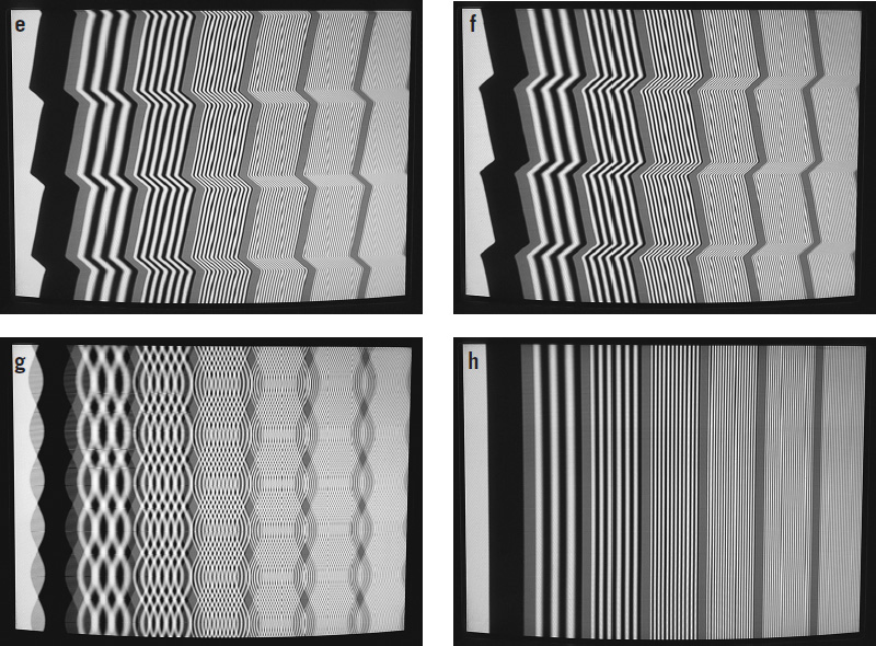
FIGURE 13-23 (a) A multiburst test signal with the video processor’s modulation signal at C34 turned off. (b) Sine-wave modulation. (c) Triangle-wave modulation. (d) Square-wave modulation. (e) Sawtooth-wave modulation. (f Second sawtooth-wave modulation. (g) Interleaved sine-wave pattern. (h) No modulation.
Figure 13-23b–f shows the effects of connecting a 1.2 volt peak-to-peak signal at approximately 240 Hz with differently shaped waveforms. Figure 13-23g shows what happens when the oscillator frequency is set to an odd multiple of the frame rate (e.g., 29.97 Hz), and an interleaved scrambling pattern is provided. Approximately, a frequency of 270 Hz or 210 Hz may be applied to result in an interleaved pattern. Again, the amplitude of the sinewave signal is 1.2 volts peak to peak.
Other types of signals may be used for modulating or scrambling the TV signal. For example, an audio signal from a radio or an audio player may be used. Random-noise generators may also be connected to the C34. A general block layout of the video processor is shown in Figure 13-24, and a picture of its breadboard is shown in Figure 13-25.

FIGURE 13-24 Block layout of the video processor.

FIGURE 13-25 Copper-clad breadboard of the video processor.
As mentioned previously, this video processor project is probably more suitable for the advanced hobbyist. Generally, the signal leads are kept short. Alternatively, from a low-resistance drive such as from the slider of VR2A, the lead can be long when it is kept away from other signal lines and kept close to the ground plane for shielding.
References
1. K. Blair Benson and Jerry Whitaker, Television Engineering Handbook. New York: McGraw-Hill, 1992.
2. Howard W. Sams, Color TV Training Manual, 4th ed. Indianapolis: Howard W. Sams Co., Inc., 1977.
3. Howard W. Coleman, ed., Color Television: The Business of Colorcasting. New York: Hastings House, 1968.
4. Dragnet, the TV series, 1966–1970.
5. John O. Ryan, Ronald Quan, James R. Holzgrafe, and Peter J. Wonfor, “Method and Apparatus for Scrambling and Descrambling of Video Signal with Edge Fill,” United States Patent Number 5,438,620, filed February 28, 1994.