
4
The Power MOSFET
School of Electrical Engineering and Computer Science, University of Central Florida, 4000 Central Florida Blvd., Orlando, Florida, USA
4.1 Introduction
4.2 Switching in Power Electronic Circuits
4.3 General Switching Characteristics
4.3.1 The Ideal Switch
4.3.2 The Practical Switch
4.4 The Power MOSFET
4.4.1 MOSFET Structure
4.4.2 MOSFET Regions of Operation
4.4.3 MOSFET Switching Characteristics
4.4.4 MOSFET PSPICE Model
4.1 Introduction
In this chapter, an overview of power MOSFET (metal oxide semiconductor field effect transistor) semiconductor switching devices will be given. The detailed discussion of the physical structure, fabrication, and physical behavior of the device and packaging is beyond the scope of this chapter. The emphasis here will be given on the terminal i-v switching characteristics of the available device, turn-on, and turn-off switching characteristics, PSPICE modeling and its current, voltage, and switching limits. Even though, most of today's available semiconductor power devices are made of silicon or germanium materials, other materials such as gallium arsenide, diamond, and silicon carbide are currently being tested.
One of the main contributions that led to the growth of the power electronics field has been the unprecedented advancement in the semiconductor technology, especially with respect to switching speed and power handling capabilities. The area of power electronics started by the introduction of the silicon controlled rectifier (SCR) in 1958. Since then, the field has grown in parallel with the growth of the power semiconductor device technology. In fact, the history of power electronics is very much connected to the development of switching devices and it emerged as a separate discipline when high power bipolar junction transistors (BJTs) and MOSFETs devices where introduced in the 1960s and 1970s. Since then, the introduction of new devices has been accompanied with dramatic improvement in power rating and switching performance. Because of their functional importance, drive complexity, fragility, cost, power electronic design engineer must be equipped with the thorough understanding of the device operation, limitation, drawbacks, and related reliability and efficiency issues.
In the 1980s, the development of power semiconductor devices took an important turn when new process technology was developed that allowed the integration of MOS and BJT technologies on the same chip. Thus far, two devices using this new technology have been introduced: integrated gate bipolar transistor (IGBT) and MOS controlled thyristor (MCT). Many of the IC processing methods and equipment have been adopted for the development of power devices. However, unlike microelectronic IC's which process information, power devices IC's process power, hence, their packaging and processing techniques are quite different. Power semiconductor devices represent the “heart” of modern power electronics, with two major desirable characteristics of power semiconductor devices that guided their development are: the switching speed and power handling capabilities.
The improvement of semiconductor processing technology along with manufacturing and packaging techniques has allowed power semiconductor development for high voltage and high current ratings and fast turn-on and turn-off characteristics. Today, switching devices are manufactured with amazing power handling capabilities and switching speeds as will be shown later. The availability of different devices with different switching speed, power handling capabilities, size, cost, … etc. make it possible to cover many power electronics applications. As a result, trade-offs are made when it comes to selecting power devices.
4.2 Switching in Power Electronic Circuits
As stated earlier, the heart of any power electronic circuit is the semiconductor-switching network. The question arises here is do we have to use switches to perform electrical power conversion from the source to the load? The answer of course is no, there are many circuits which can perform energy conversion without switches such as linear regulators and power amplifiers. However, the need for using semiconductor devices to perform conversion functions is very much related to the converter efficiency. In power electronic circuits, the semiconductor devices are generally operated as switches, i.e. either in the on-state or the off-state. This is unlike the case in power amplifiers and linear regulators where semiconductor devices operate in the linear mode. As a result, very large amount of energy is lost within the power circuit before the processed energy reaches the output. The need to use semiconductor switching devices in power electronic circuits is their ability to control and manipulate very large amounts of power from the input to the output with a relatively very low power dissipation in the switching device. Hence, resulting in a very high efficient power electronic system.
Efficiency is considered as an important figure of merit and has significant implications on the overall performance of the system. Low efficient power systems means large amounts of power being dissipated in a form of heat, resulting in one or more of the following implications:
1. Cost of energy increases due to increased consumption.
2. Additional design complications might be imposed, especially regarding the design of device heat sinks.
3. Additional components such as heat sinks increase cost, size, and weight of the system, resulting in low power density.
4. High power dissipation forces the switch to operate at low switching frequency, resulting in limited bandwidth, slow response, and most importantly, the size and weight of magnetic components (inductors and transformers), and capacitors remain large. Therefore, it is always desired to operate switches at very high frequencies. But, we will show later that as the switching frequency increases, the average switching power dissipation increases. Hence, a trade-off must be made between reduced size, weight, and cost of components vs reduced switching power dissipation, which means inexpensive low switching frequency devices.
For more than forty years, it has been shown that in order to achieve high efficiency, switching (mechanical or electrical) is the best possible way to accomplish this. However, unlike mechanical switches, electronic switches are far more superior because of their speed and power handling capabilities as well as reliability.
We should note that the advantages of using switches don't come at no cost. Because of the nature of switch currents and voltages (square waveforms), normally high order harmonics are generated in the system. To reduce these harmonics: additional input and output filters are normally added to the system. Moreover, depending on the device type and power electronic circuit topology used, driver circuit control and circuit protection can significantly increase the complexity of the system and its cost.
EXAMPLE 4.1 The purpose of this example is to investigate the efficiency of four different power circuits whose functions are to take in power from 24 volts dc source and deliver a 12 volts dc output to a 6 Ω resistive load. In other words, the tasks of these circuits are to serve as dc transformer with a ratio of 2:1. The four circuits are shown in Fig. 4.1a–d representing voltage divider circuit, zener-regulator, transistor linear regulator, and switching circuit, respectively. The objective is to calculate the efficiency of those four power electronic circuits.
SOLUTION.
Voltage Divider DC Regulator The first circuit is the simplest forming a voltage divider with R = RL = 6Ω and Vo = 12 volts. The efficiency defined as the ratio of the average load power, PL, to the average input power, Pin
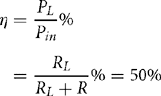
In fact efficiency is simply Vo/Vin%. As the output voltage becomes smaller, the efficiency decreases proportionally.
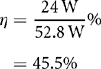
Zener DC Regulator Since the desired output is 12 V, we select a zener diode with zener breakdown VZ= 12 V. Assume the zener diode has the i–v characteristic shown in Fig. 4.1e since RL = 6ω, the load current, IL, is 2 A. Then we calculate R for IZ = 0.2 A (10% of the load current). This results in R = 5.27Ω. Since the input power is Pin = 2.2A × 24V = 52.8W and the output power is Pout = 24W. The efficiency of the circuit is given by,
Transistor DC Regulator It is clear from Fig. 4.1c that for Vo = 12 V, the collector emitter voltage must be around 12 V. Hence, the control circuit must provide base current, IB to put the transistor in the active mode with VCE ≈ 12 V. Since the load current is 2 A, then collector current is approximately 2 A (assume small IB). The total power dissipated in the transistor can be approximated by the following equation:
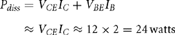
Therefore, the efficiency of the circuit is 50%.
Switching DC Regulator Let us consider the switching circuit of Fig. 4.1d by assuming the switch is ideal and periodically turned on and off is shown in Fig. 4.1f. The output voltage waveform is shown in Fig. 4.1f. Even though the output voltage is not constant or pure dc, its average value is given by,
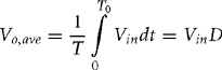
where D is the duty ratio equals the ratio of the on-time to the switching period. For Vo,ave = 12 V, we set D = 0.5, i.e. the switch has a duty cycle of 0.5 or 50%. In case, the average output power is 48 W and the average input power is also 48 W, resulting in 100% efficiency! This is of course because we assumed the switch is ideal. However, let us assume a BJT switch is used in the above circuit with VCE,sat= 1V and IB is small, then the average power loss across the switch is approximately 2W, resulting in overall efficiency of 96%. Of course the switching circuit given in this example is over simplified, since the switch requires additional driving circuitry that was not shown, which also dissipates some power. But still, the example illustrates that high efficiency can be acquired by switching power electronic circuits when compared to the efficiency of linear power electronic circuits. Also, the difference between the linear circuit in Figs. 4.1b and c and the switched circuit of Fig. 4.1d is that the power delivered to the load in the later case in pulsating between zero and 96 watts. If the application calls for constant power delivery with little output voltage ripple, then an LC filter must be added to smooth out the output voltage.
The final observation is regarding what is known as load regulation and line regulation. The line regulation is defined as the ratio between the change in output voltage, ΔVo, with respect to the change in the input voltage ΔVin This is a very important parameter in power electronics since the dc input voltage is obtained from a rectified line voltage that normally changes by ± 20%. Therefore, any off-line power electronics circuit must have a limited or specified range of line regulation. If we assume the input voltage in Figs. 4.1a,b is changed by 2V, i.e. ΔVin = 2V, with RL unchanged, the corresponding change in the output voltage ΔVo is 1V and 0.55V, respectively. This is considered very poor line regulation. Figures 4.1c,d have much better line and load regulations since the closed-loop control compensate for the line and load variations.
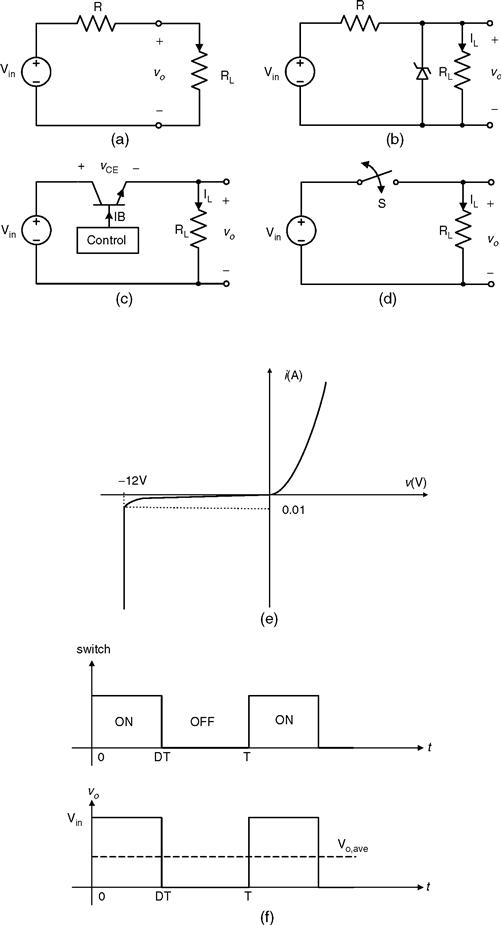
FIGURE 4.1 (a) Voltage divider; (b) zener regulator; (c) transistor regulator; (d) switching circuit; (e) i-v zener diode characteristics; and (f) switching waveform for S and corresponding output waveform.
4.3 General Switching Characteristics
4.3.1 The Ideal Switch
It is always desired to have the power switches perform as close as possible to the ideal case. Device characteristically speaking, for a semiconductor device to operate as an ideal switch, it must possess the following features:
1. No limit on the amount of current (known as forward or reverse current) the device can carry when in the conduction state (on-state);
2. No limit on the amount of the device-voltage ((known as forward or reverse blocking voltage) when the device is in the non-conduction state (off-state);
3. Zero on-state voltage drop when in the conduction state;
4. Infinite off-state resistance, i.e. zero leakage current when in the non-conduction state; and
5. No limit on the operating speed of the device when changes states, i.e. zero rise and fall times.
The switching waveforms for an ideal switch is shown in Fig. 4.2, where isw and vsw are the current through and the voltage across the switch, respectively.
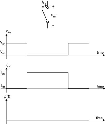
FIGURE 4.2 Ideal switching current, voltage, and power waveforms.
Both during the switching and conduction periods, the power loss is zero, resulting in a 100% efficiency, and with no switching delays, an infinite operating frequency can be achieved. In short, an ideal switch has infinite speed, unlimited power handling capabilities, and 100% efficiency. It must be noted that it is not surprising to find semiconductor-switching devices that can almost, for all practical purposes, perform as ideal switches for number of applications.
4.3.2 The Practical Switch
The practical switch has the following switching and conduction characteristics:
1. Limited power handling capabilities, i.e. limited conduction current when the switch is in the on-state, and limited blocking voltage when the switch is in the off −state.
2. Limited switching speed that is caused by the finite turn-on and turn-off times. This limits the maximum operating frequency of the device.
3. Finite on-state and off-state resistance's i.e. there exists forward voltage drop when in the on-state, and reverse current flow (leakage) when in the off state.
4. Because of characteristics 2 and 3 above, the practical switch experiences power losses in the on and the off states (known as conduction loss), and during switching transitions (known as switching loss). Typical switching waveforms of a practical switch are shown in Fig. 4.3a.
The average switching power and conduction power losses can be evaluated from these waveforms. We should point out the exact practical switching waveforms vary from one device to another device, but Fig. 4.3a is a reasonably good representation. Moreover, other issues such as temperature dependence, power gain, surge capacity, and over voltage capacity must be considered when addressing specific devices for specific applications. A useful plot that illustrates how switching takes place from on to off and vice versa is what is called switching trajectory, which is simply a plot of isw vs vsw. Figure 4.3b shows several switching trajectories for the ideal and practical cases under resistive loads.
EXAMPLE 4.2 Consider a linear approximation of Fig. 4.3a as shown in Fig. 4.4a: (a) Give a possible circuit implementation using a power switch whose switching waveforms are shown in Fig. 4.4a, (b) Derive the expressions for the instantaneous switching and conduction power losses and sketch them, (c) Determine the total average power dissipated in the circuit during one switching frequency, and (d) The maximum power.
SOLUTION. (a) First let us assume that the turn-on time, ton, and turn-off time, toff, the conduction voltage VON, and the leakage current, IOFF, are part of the switching characteristics of the switching device and have nothing to do with circuit topology.
When the switch is off, the blocking voltage across the switch is VOFF that can be represented as a dc voltage source of value VOFF reflected somehow across the switch during the off-state. When the switch is on, the current through the switch equals ION, hence, a dc current is needed in series with the switch when it is in the on-state. This suggests that when the switch turns off again, the current in series with the switch must be diverted somewhere else (this process is known as commutation). As a result, a second switch is needed to carry the main current from the switch being investigated when it's switched off. However, since isw and vsw are linearly related as shown in Fig. 4.4b, a resistor will do the trick and a second switch is not needed. Figure 4.4 shows a one-switch implementation with S, the switch and R represents the switched-load.
(b) The instantaneous current and voltage waveforms during the transition and conduction times are given as follows
FIGURE 4.3 (a) Practical switching current, voltage, and power waveforms and (b) switching trajectory.
FIGURE 4.4 Linear approximation of typical current and voltage switching waveforms.
It can be shown that if we assume ION ![]() IOFF and VOFF
IOFF and VOFF ![]() VON, then the instantaneous power, p(t) = iswvsw can be given as follows,
VON, then the instantaneous power, p(t) = iswvsw can be given as follows,
Figure 4.4c shows a plot of the instantaneous power where the maximum power during turn-on and off is VOFFION/4.
(c) The total average dissipated power is given by
The evaluation of the above integral gives
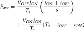
The first expression represents the total switching loss, whereas the second expression represents the total conduction loss over one switching cycle. We notice that as the frequency increases, the average power increases linearly. Also the power dissipation increases with the increase in the forward conduction current and the reverse blocking voltage.
(d) The maximum power occurs at the time when the first derivative of p(t) during switching is set to zero, i.e.
![]()
solve the above equation for tmax, we obtain values at turn on and off, respectively,
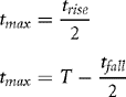
Solving for the maximum power, we obtain
![]()
4.4 The Power MOSFET
Unlike the bipolar junction transistor (BJT), the MOSFET device belongs to the Unipolar Device family, since it uses only the majority carriers in conduction. The development of the metal oxide semiconductor technology for microelectronic circuits opened the way for developing the power metal oxide semiconductor field effect transistor (MOSFET) device in 1975. Selecting the most appropriate device for a given application is not an easy task, requiring knowledge about the device characteristics, its unique features, innovation, and engineering design experience. Unlike low power (signal devices), power devices are more complicated in structure, driver design, and understanding of their operational i–v characteristics. This knowledge is very important for power electronics engineer to design circuits that will make these devices close to ideal. The device symbol for a p- and n-channel enhancement and depletion types are shown in Fig. 4.5. Figure 4.6 shows the i–v characteristics for the n-channel enhancement-type MOSFET. It is the fastest power switching device with switching frequency more than 1 MHz, with voltage power ratings up to 1000 V and current rating as high as 300 A.
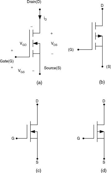
FIGURE 4.5 Device symbols: (a) n-channel enhancement-mode; (b) p-channel enhancement-mode; (c) n-channel depletion-mode; and (d) p-channel depletion-mode.
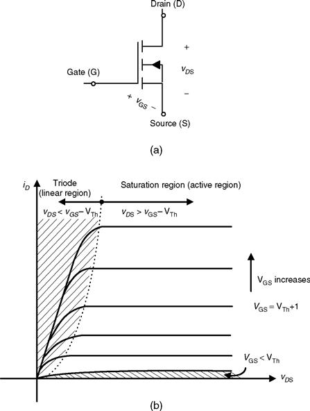
FIGURE 4.6 (a) n-Channel enhancement-mode MOSFET and (b) its iD vs vDS characteristics.
MOSFET regions of operations will be studied shortly.
4.4.1 MOSFET Structure
Unlike the lateral channel MOSFET devices used in many IC technology in which the gate, source, and drain terminals are located in the same surface of the silicon wafer, power MOSFET use vertical channel structure in order to increase the device power rating [1]. In the vertical channel structure, the source and drain are in opposite side of the silicon waver. Figure 4.7a shows vertical cross-sectional view for a power MOSFET. Figure 4.7b shows a more simplified representation. There are several discrete types of the vertical structure power MOSFET available commercially today such as V-MOSFET, U-MOSFET, D-MOSFET, and S-MOSFET [1, 2]. The P–N junction between p-base (also referred to as body or bulk region) and the n-drift region provide the forward voltage blocking capabilities. The source metal contact is connected directly to the p-base region through a break in the n+ source region in order to allow for a fixed potential to p-base region during the normal device operation. When the gate and source terminal are set the same potential (VGS = 0), no channel is established in the p-base region, i.e. the channel region remain unmodulated. The lower doping in the n-drift region is needed in order to achieve higher drain voltage blocking capabilities. For the drain–source current, ID, to flow, a conductive path must be established between the n+ and n− regions through the p-base diffusion region.

FIGURE 4.7 (a) Vertical cross-sectional view for a power MOSFET and (b) simplified representation.
A. On-state Resistance
When the MOSFET is in the on-state (triode region), the channel of the device behaves like a constant resistance, RDS(ON) that is linearly proportional to the change between vDS and iD as given by the following relation:
![]() (4.1)
(4.1)
The total conduction (on-state) power loss for a given MOSFET with forward current ID and on-resistance RDS(on) is given by,
![]() (4.2)
(4.2)
The value of RDS(on) can be significant and it varies between tens of milliohms and a few ohms for low-voltage and high-voltage MOSFETS, respectively. The on-state resistance is an important data sheet parameter, since it determines the forward voltage drop across the device and its total power losses.
Unlike the current-controlled bipolar device, which requires base current to allow the current to flow in the collector, the power MOSFET device is a voltage-controlled unipolar device and requires only a small amount of input (gate) current. As a result, it requires less drive power than the BJT. However, it is a non-latching current like the BJT i.e. a gate source voltage must be maintained. Moreover, since only majority carriers contribute to the current flow, MOSFETs surpass all other devices in switching speed with switching speeds exceeding a few megahertz. Comparing the BJT and the MOSFET, the BJT has higher power handling capabilities and smaller switching speed, while the MOSFET device has less power handling capabilities and relatively fast switching speed. The MOSFET device has higher on-state resistor than the bipolar transistor. Another difference is that the BJT parameters are more sensitive to junction temperature when compared to the MOSFET, and unlike the BJT, MOSFET devices do not suffer from second breakdown voltages, and sharing current in parallel devices is possible.
B. Internal Body Diode
The modern power MOSFET has an internal diode called a body diode connected between the source and the drain as shown in Fig. 4.8a. This diode provides a reverse direction for the drain current, allowing a bi-directional switch implementation. Even though the MOSFET body diode has adequate current and switching speed ratings, in some power electronic applications that require the use of ultra-fast diodes, an external fast recovery diode is added in anti-parallel fashion after blocking the body diode by a slow recovery diode as shown in Fig. 4.8b.
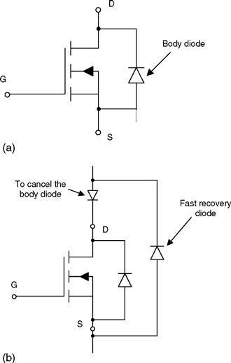
FIGURE 4.8 (a) MOSFET Internal body diode and (b) implementation of a fast body diode.
C. Internal Capacitors
Another important parameter that effect the MOSFET's switching behavior is the parasitic capacitance between the device's three terminals, namely, gate-to-source, Cgs, gate-to-drain, Cgd, and drain-to-source (Cds) capacitance as shown in Fig. 4.9a. Figure 4.9b shows the physical representation of these capacitors. The values of these capacitances are non-linear and a function of device structure, geometry, and bias voltages. During turn on, capacitor Cgd and Cgs must be charged through the gate, hence, the design of the gate control circuit must take into consideration the variation in this capacitance (Fig. 4.9b). The largest variation occurs in the gate-to-drain capacitance as the drain-to-gate voltage varies. The MOSFET parasitic capacitance are given in terms of the device data sheet parameters Ciss, Coss, and Crss as follows,
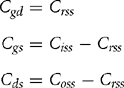
where Crss = small-signal reverse transfer capacitance.
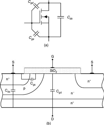
FIGURE 4.9 (a) Equivalent MOSFET representation including junction capacitances and (b) representation of this physical location.
Ciss = small-signal input capacitance with the drain and source terminals are shorted.
Coss = small-signal output capacitance with the gate and source terminals are shorted.
The MOSFET capacitances Cgs, Cgd, and Cds are non-linear and function of the dc bias voltage. The variations in Coss and Ciss are significant as the drain-to-source and gate-to-source voltages cross zero, respectively. The objective of the drive circuit is to charge and discharge the gate-to-source and gate-to-drain parasitic capacitance to turn on and off the device, respectively.
In power electronics, the aim is to use power-switching devices to operate at higher and higher frequencies. Hence, size and weight associated with the output transformer, inductors, and filter capacitors will decrease. As a result, MOSFETs are used extensively in power supply design that requires high switching frequencies including switching and resonant mode power supplies and brushless dc motor drives. Because of its large conduction losses, its power rating is limited to a few kilowatts. Because of its many advantages over the BJT devices, modern MOSFET devices have received high market acceptance.
4.4.2 MOSFET Regions of Operation
Most of the MOSFET devices used in power electronics applications are of the n-channel, enhancement-type like that which is shown in Fig. 4.6a. For the MOSFET to carry drain current, a channel between the drain and the source must be created. This occurs when the gate-to-source voltage exceeds the device threshold voltage, VTh. For vGS > VTh, the device can be either in the triode region, which is also called “constant resistance” region, or in the saturation region, depending on the value of vDS. For given vGS , with small vDS ( vDS < vGS − VTh), the device operates in the triode region(saturation region in the BJT), and for larger vDS(vDS > vGS –VTh), the device enters the saturation region (active region in the BJT). For vGS < VTh, the device turns off, with drain current almost equals zero. Under both regions of operation, the gate current is almost zero. This is why the MOSFET is known as a voltage-driven device, and therefore, requires simple gate control circuit.
The characteristic curves in Fig. 4.6b show that there are three distinct regions of operation labeled as triode region, saturation region, and cut-off-region. When used as a switching device, only triode and cut-off regions are used, whereas, when it is used as an amplifier, the MOSFET must operate in the saturation region, which corresponds to the active region in the BJT.
The device operates in the cut-off region (off-state) when vGS < VTh, resulting in no induced channel. In order to operate the MOSFET in either the triode or saturation region, a channel must first be induced. This can be accomplished by applying gate-to-source voltage that exceeds VTh, i.e.
![]()
Once the channel is induced, the MOSFET can either operate in the triode region (when the channel is continuous with no pinch-off, resulting in the drain current proportioned to the channel resistance) or in the saturation region (the channel pinches off, resulting in constant ID). The gate-to-drain bias voltage (vGD) determines whether the induced channel enter pinch-off or not. This is subject to the following restriction.
For triode mode of operation, we have

And for the saturation region of operation, Pinch-off occurs when vGD = VTh.
![]()
In terms of vDS, the above inequalities may be expressed as follows:
1. For triode region of operation
![]() (4.3)
(4.3)
2. For saturation region of operation
![]() (4.4)
(4.4)
3. For cut-off region of operation
![]() (4.5)
(4.5)
It can be shown that drain current, iD, can be mathematically approximated as follows:
![]() (4.6)
(4.6)
![]() (4.7)
(4.7)
where, ![]()
μn = electron mobility
COX = oxide capacitance per unit area
L = length of the channel
W = width of the channel.
Typical values for the above parameters are given in the PSPICE model discussed later. At the boundary between the saturation (active) and triode regions, we have,
![]() (4.8)
(4.8)
Resulting in the following equation for iD,
![]() (4.9)
(4.9)
The input transfer characteristics curve for iD and vS. vGS is when the device is operating in the saturation region shown in Fig. 4.10.
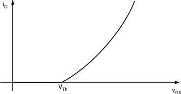
FIGURE 4.10 Input transfer characteristics for a MOSFET device when operating in the saturation region.
The large signal equivalent circuit model for a n-channel enhancement-type MOSFET operating in the saturation mode is shown in Fig. 4.11. The drain current is represented by a current source as the function of VTh and vGS.
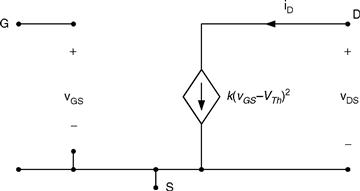
FIGURE 4.11 Large signal equivalent circuit model.
If we assume that once the channel is pinched-off, the drain–source current will no longer be constant but rather depends on the value of vDS as shown in Fig. 4.12. The increased value of vDS results in reduced channel length, resulting in a phenomenon known as channel-length modulation [3, 4]. If the vDS –iD lines are extended as shown in Fig. 4.12, they all intercept the vDS-axis at a single point labeled − 1/λ, where λ is a positive constant MOSFET parameter. The term (1 + λ vDS) is added to the iD equation in order to account for the increase in iD due to the channel-length modulation, i.e. iD is given by,
![]() (4.10)
(4.10)
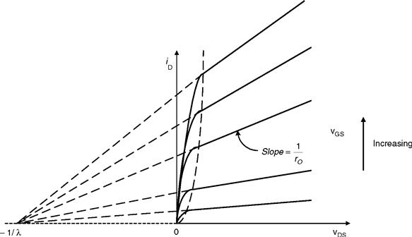
FIGURE 4.12 MOSFET characteristics curve including output resistance.
From the definition of the ro given in Eq. (4.1), it is easy to show the MOSFET output resistance which can be expressed as follows:
![]() (4.11)
(4.11)
If we assume the MOSFET is operating under small signal condition, i.e. the variation in vGS on iD vs vGS is in the neighborhood of the dc operating point Q at iD and vGS as shown in Fig. 4.13. As a result, the iD current source can be represented by the product of the slope gm and vGS as shown in Fig. 4.14.
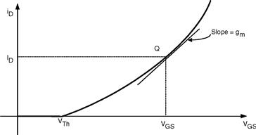
FIGURE 4.13 Linearized iD vs vGS curve with operating dc point (Q).
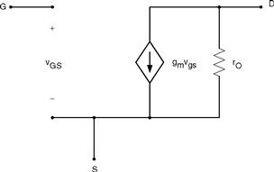
FIGURE 4.14 Small-signal equivalent circuit including MOSFET output resistance.
4.4.3 MOSFET Switching Characteristics
Since the MOSFET is a majority carrier transport device, it is inherently capable of a high frequency operation [5–8]. But still the MOSFET has two limitations:
1. High input gate capacitances.
2. Transient/delay due to carrier transport through the drift region.
As stated earlier the input capacitance consists of two components: the gate-to-source and gate-to-drain capacitances. The input capacitances can be expressed in terms of the device junction capacitances by applying Miller theorem to Fig. 4.15a. Using Miller theorem, the total input capacitance, Cin, seen between the gate-to-source is given by,
![]() (4.12)
(4.12)
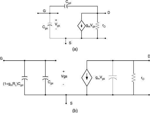
FIGURE 4.15 (a) Small-signal model including parasitic capacitances and (b) equivalent circuit using Miller theorem.
The frequency response of the MOSFET circuit is limited by the charging and discharging times of Cin. Miller effect is inherent in any feedback transistor circuit with resistive load that exhibits a feedback capacitance from the input and output. The objective is to reduce the feedback gate-to-drain resistance. The output capacitance between the drain-to-source, Cds, does not affect the turn-on and turn-off MOSFET switching characteristics. Figure 4.16 shows how Cgd and Cgs vary under increased drain–source, vDs, voltage.
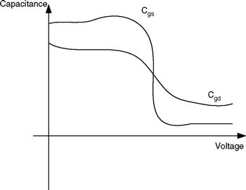
FIGURE 4.16 Variation of Cgd and Cgs as a function of vDS.
In power electronics applications, the power MOSFETs are operated at high frequencies in order to reduce the size of the magnetic components. In order to reduce the switching losses, the power MOSFETs are maintained in either the on-state (conduction state) or the off-state (forward blocking) state.
It is important we understand the internal device behavior; therefore, the parameters that govern the device transition from the on-state and off-states. To investigate the on and off switching characteristics, we consider the simple power electronic circuit shown in Fig. 4.17a under inductive load. The fly back diode D is used to pick up the load current when the switch is off. To simplify the analysis we will assume the load inductance is L0 large enough so that the current through it is constant as shown in Fig. 4.17b.
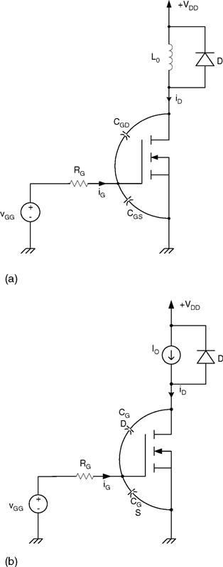
FIGURE 4.17 (a) Simplified equivalent circuit used to study turn-on and turn-off characteristics of the MOSFET and (b) simplified equivalent circuit.
A. Turn-on Analysis
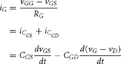
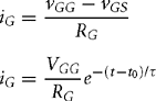
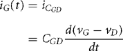
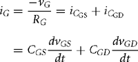
Let us assume initially the device is off, the load current, I0 flows through D as shown in the Fig. 4.18a vGG = 0. The voltage vDS = VDD and iG = iD At t = t0, the voltage vGG is applied as shown in Fig. 4.19a. The voltage across CGS starts charging through RG. The gate–source voltage, vGS, controls the flow of the drain-to-source current iD. Let us assume that for t0 = t< t1, vGS < VTh, i.e. the MOSFET remains in the cut-off region with iD = 0, regardless of vDS The time interval (t1,t0) represents the delay turn-on time needed to change CGS from zero to VTh The expression for the time interval Δt10 = t1 –t0 can be obtained as follows: The gate current is given by,
 (4.13)
where vG and vD are gate-to-ground and drain-to-ground voltages, respectively.
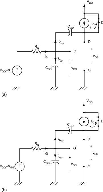
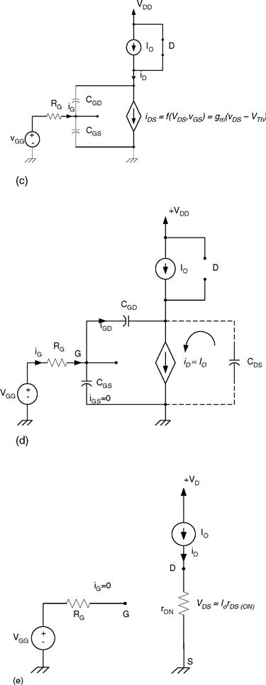
FIGURE 4.18 Equivalent modes: (a) MOSFET is in the off-state for t < t0, vGG = 0, vDS = VDD, i G = 0, iD = 0; (b) MOSFET in the off-state with vGS < VTh for t1 >t > t0 ; (c) vGS > VTh, iD < I0 for t1 < t< t2, (d) vGS > VTh, iD = I0 for t2 = t< t3 ; and (e) VGS > VTh, iD = Io for t3 = t < t4.
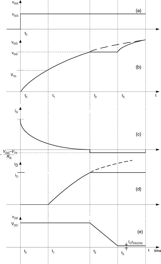
FIGURE 4.19 Turn-on waveform switiching.
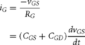
Since we have vG = vGS, vD = +VDD, then iG is given by
![]() (4.14)
(4.14)
From Eqs. (4.13) and (4.14), we obtain,
![]() (4.15)
(4.15)
Solving Eq. (4.15) for vGS(t) for t > t0 with vGS(t0) = 0, we obtain,
![]() (4.16)
(4.16)
![]()
The gate current, iG , is given by,
 (4.17)
As long as vGS < VTh, iD remains zero. At t= t1, vGS reaches VTh causing the MOSFET to start conducting. Waveforms for iG and vGS are shown in Fig. 4.19. The time interval (t1 –t0) is given by,
![]()
Δt10 represents the first delay interval in the turn-on process. For t > t1 with vGS > VTh, the device starts conducting and its drain current is given as a function of vGS and VTh. In fact iD starts flowing exponentially from zero as shown in Fig. 4.19d. Assume the input transfer characteristics for the MOSFET is limited as shown in Fig. 4.20 with slope of gm that is given by
![]() (4.18)
(4.18)
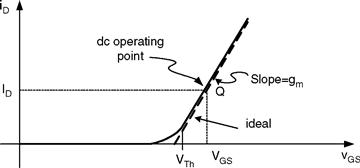
FIGURE 4.20 Input transfer characteristics.
The drain current can be approximately given as follows:
![]() (4.19)
(4.19)
As long as iD(t) < I0, D remains on and vDS = VDD as shown in Fig. 4.18c.
The equation for vGS(t) remains the same as in Eq. (4.16), hence, Eq. (4.19) results in iD(t) given by,
![]() (4.20)
(4.20)
The gate current continues to decrease exponentially as shown in Fig. 4.19c. At t = t2, iD reaches its maximum value of I0 turning D off. The time interval Δt21 = (t2 –t1) is obtained from Eq. (4.20) by setting iD(t2) = I0
![]() (4.21)
(4.21)
For t > t2 the diode turns off and iD ≈ I0 as shown in Fig. 4.18d. Since the drain current is nearly a constant, then the gate–source voltage is also constant according to the input transfer characteristic of the MOSFET, i.e.
![]() (4.22)
(4.22)
Hence,
![]() (4.23)
(4.23)
At t = t2, iG (t) is, iG(t) is given by,
![]() (4.24)
(4.24)
Since the time constant t is very small, it is safe to assume vGS(t2) reaches its maximum, i.e.
![]()
and
![]()
For t2 ≤ t < t3, the diode turns off the load current I0 (drain current iD), which starts discharging the drain-to-source capacitance.
Since vGS is constant, the entire gate current flows through CGD, resulting in the following relation,
Since vG is constant and vs = 0, we have
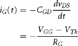
Solving for vDS(t) for t > t2, with vDS (t2) = VDD, we obtain
![]() (4.25)
(4.25)
This is a linear discharge of CGD as shown in Fig. 4.19e
The time interval Δt32 = (t3–t2) is determined by assuming that at t = t3, the drain-to-source voltage reaches its minimum value determined by its on resistance, vDS (ON) i · e · vDS (ON) is given by,
![]()
For t > t3, the gate current continues to charge CGD and since vDS is constant, vGS starts charging at the same rate as in interval t0 ≤ t <t1, i.e.
![]()
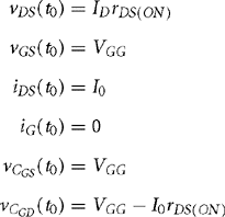
The gate voltage keeps increasing exponentially until t = t3 when it reaches VGG, at which iG = 0 and the device fully turns on as shown in Fig. 4.18e.
The equivalent circuit model when the MOSFET is completely turned on is for t > t1. At this time, the capacitors CGS and CGD are charged with VGG and (I0 rds(ON) –VGG), respectively.
The time interval Δt32 = (t3–t2) is obtained by evaluating vDS at t = t3 as follows
 (4.26)
Hence, Δt32 = (t3 –t2) is given by,
![]() (4.27)
(4.27)
The total delay in turning on the MOSFET is given by
![]() (4.28)
(4.28)
Notice the MOSFET sustains high voltage and current simultaneously during intervals Δt21 and Δt32 This results in large power dissipation during turn on, that contributes to the overall switching losses. The smaller the RG, the smaller Δt21 and Δt32 become.
B. Turn-off Characteristics
To study the turn-off characteristic of the MOSFET, we will consider Fig. 4.17b again by assuming the MOSFET is ON and in steady state at t > t0 with the equivalent circuit of Fig. 4.18e. Therefore, at t = t0 we have the following initial conditions.
 (4.29)
At t = t0, the gate voltage, vGG ( t ) is reduced to zero as shown in Fig. 4.2 la. The equivalent circuit at t > t0 is shown in Fig. 4.22a.
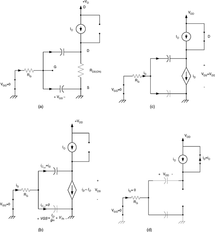
FIGURE 4.22 Equivalent circuits: (a) t0 = t <t1 ; (b) t1 = t<t2 ; (c) t2 = t<t3 ; and (d) t3 = t <t4.
If we assume the drain-to-source voltage remains constant, CGS and CGD are discharging through RG as governed by the following relations
Since vDS is assumed constant, then iG becomes,
 (4.30)
Hence, evaluating for vGS for t ≤ t0, we obtain
![]() (4.31)
(4.31)
where,
![]()
As vGS continues to decrease exponentially, drawing current from CGD will reach a constant value at which drain current is fixed, i.e. ID = I0. From the input transfer characteristics, the value of vGS when ID = I0 is given by,
![]() (4.32)
(4.32)
The time interval Δt10 = t1 –t0 can be obtained easily by setting Eq. (4.31) to (4.32) at t = t1.
The gate current during the t1 ≤ t < t1 is given by
![]() (4.33)
(4.33)
Since, for t2-t1, the gate-to-source voltage is constant and equals vGS(t1) = (I0 /gm) + VTh as shown in Fig. 4.21b, then the entire gate current is being drawn from CGD, hence,
![]()
Integrating both sides of the above equation from t1 to t with vDS(t1)= –vDS(ON) , we obtain,
![]() (4.34)
(4.34)
hence, vDS charges linearly until it reaches VDD.
At t = t2, the drain-to-source voltage becomes equal to VDD, forcing D to turn on as shown in Fig. 4.22c.
The drain-to-source current is obtained from the transfer characteristics and given by
![]()
where vGS(t) is obtained from the following equation
![]() (4.35)
(4.35)
Integrate both sides from t2 to t with vGS(t2) = (I0 /gm) + VTh, we obtain the following expression for vGS(t),
![]() (4.36)
(4.36)
Hence the gate current and drain-to-source current are given by,
![]() (4.37)
(4.37)
The time interval between t2 = t < t3 is obtained by evaluating vGS(t3) = VTh, at which the drain current becomesapproximately zero and the MOSFET turn off hence,
FIGURE 4.21 Turn-off switching waveforms.
Assuming iG constant at its initial value at t = t1, i.e.
Solving for Δt32 = t3−t2 we obtain,
![]() (4.39)
(4.39)
For t > t3, the gate voltage continues to decrease exponentially to zero, at which the gate current becomes zero and CGD charges to −VDD Between t3 and t4, ID discharges to zero as shown in the equivalent circuit Fig. 4.22d.
The total turn-off time for the MOSFET is given by,
 (4.40)
The time intervals that most effect the power dissipation are Δt21 and Δt32 It is clear that in order to reduce the MOSFET ton and toff times, the gate–drain capacitance must be reduced. Readers are encouraged to see the reference by Baliga for detailed discussion on the turn-on and turn-off characteristics of the MOSFET and to explore various fabrication methods.
C. Safe Operation Area
The safe operation area (SOA) of a device provides the current and voltage limits. The device must handle to avoid destructive failure. Typical SOA for a MOSFET device is shown in Fig. 4.23. The maximum current limit while the device is on is determined by the maximum power dissipation
![]()
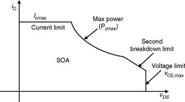
FIGURE 4.23 Safe operation area for MOSFET.
As the drain–source voltage starts increasing, the device starts leaving the on-state and enters the saturation (linear) region. During the transition time, the device exhibits large voltage and current simultaneously. At higher drain–source voltage values that approach the avalanche breakdown it is observed that power MOSFET suffers from second breakdown phenomenon. The second breakdown occurs when the MOSFET is in the blocking state (off) and a further increase in vDS will cause a sudden drop in the blocking voltage. The source of this phenomenon in MOSFET is caused by the presence of a parasitic n-type bipolar transistor as shown in Fig. 4.24.
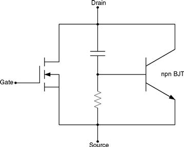
FIGURE 4.24 MOSFET equivalent circuit including the parasitic BJT.
The inherent presence of the body diode in the MOSFET structure makes the device attractive to application in which bi-directional current flow is needed in the power switches.
Today's commercial MOSFET devices have excellent high operating temperatures. The effect of temperature is more prominent on the on-state resistance as shown in Fig. 4.25.
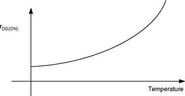
FIGURE 4.25 The on-state resistance as a fraction of temperature.
As the on-state resistance increases, the conduction losses also increase. This large vDS(ON) limits the use of the MOSFET in high voltage applications. The use of silicon carbide instead of silicon has reduced vDS(ON) by many folds.
As the device technology keeps improving in terms of improving switch speeds, increased power handling capabilities, it is expected that the MOSFET will continue to replace BJTs in all types of power electronics systems.
4.4.4 MOSFET PSPICE Model
The PSPICE simulation package has been used widely by electrical engineers as an essential software tool for circuit design. With the increasing number of devices available in the market place, PSPICE allows for the accurate extraction and understanding of various device parameters and their variation effect on the overall design prior to their fabrication. Today's PSPICE library is rich with numerous commercial MOSFET models. This section will give a brief overview of how the MOSFET model is implemented in PSPICE. A brief overview of the PSPICE modeling of the MOSFET device will be given here.
A. PSPICE Static Model
There are four different types of MOSFET models that are also known as levels. The simplest MOSFET model is called LEVEL1 model and is shown in Fig. 4.26 [9, 10].
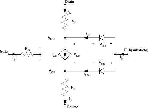
FIGURE 4.26 PSPICE LEVEL1 MOSFET static model.
LEVEL2 model uses the same parameters as LEVEL1, but it provides a better model for Ids by computing the model coefficients KP, VTO, LAMBDA, PHI, and GAMMA directly from the geometrical, physical, and technological parameters [10]. LEVEL3 is used to model the short-channel devices and LEVEL4 represents the Berkeley Short-channel IGFET model (BSIM-model).
The triode region, vGS > VTh and vDS < vGS and vDS < vGS −VTh the drain current is given by,
![]() (4.41)
(4.41)
In the saturation (linear) region, where vGS > VTh and vDS > vGS − VTh, the drain current is given by
![]() (4.42)
(4.42)
where Kp is the transconductance and Xjl is the lateral diffusion.
The threshold voltage, VTh, is given by,
![]() (4.43)
(4.43)
where,VT0 = Zero-bias threshold voltage.
δ = Body-effect parameter.
ϕp = Surface inversion potential.
Typically, Xij ![]() L and λ ≈ 0.
L and λ ≈ 0.
The term (1 + λVDS) is included in the model as empirical connection to model the effect of the output conductance when the MOSFET is operating in triode region, λ is known as the channel-length modulation parameter.
When the bulk and source terminals are connected together, i.e. VBS = 0, the device threshold voltage equals the zero-bias threshold voltage, i.e.
![]()
VT0 is positive for the n-channel enhancement-mode devices and negative for the n-channel depletion-mode devices.
The parameters Kp, VT0, δ, ϕ are electrical parameters that can be either specified directly in the MODEL statement under the Pspice keywords KP, VTO, GAMMA, and PHI, respectively, as shown in Table 4.1. They also can be calculated when the geometrical and physical parameters are known. The two-substrate currents that flow from the bulk to the source, IBS and from the bulk to the drain, IBD are simply diode currents, which are given by,
![]() (4.44)
(4.44)
![]() (4.45)
(4.45)
where Iss and IDS are the substrate source and substrate drain saturation currents. These currents are considered equal and given as Is in the MODEL statement with a default value of 10− 14 A. Where the equation symbols and their corresponding PSPICE parameter names are shown in Table 4.1.
TABLE 4.1 PSPICE MOSFET parameters

* These numbers indicate that this parameter is available in this level number, otherwise it is available in all levels.
In PSPICE, a MOSFET device is described by two statements: the first statement start with the letter M and the second statement starts with. Model that defines the model used in the first statement. The following syntax is used:
M<device_name> <Drain_node_number>
<Source_node_number> <Substrate_node number>
where the starting letter “M” in M<device_name> statement indicates that the device is a MOSFET and <device_name>is a user specified label for the given device, the <Model_name> is one of the hundreds of device models specified in the PSPICE library, <Model_name> the same name specified in the device name statement, <type_name> is either NMOS of PMOS, depending on whether the device is n-channel or p-channel MOS, respectively, that follows by optional list of parameter types and their values. The length L and the width W and other parameters can be specified in the M<device_name>, in the.MODEL or.OPTION statements. User may select not to include any value, and PSPICE will use the specified default values in the model. For normal operation (physical construction of the MOS devices), the source and bulk substrate nodes must be connected together. In all the PSPICE library files, a default parameter values for L, W, AS, AD, PS, PD, NRD, and NDS are included, hence, user should not specify such values in the device “M” statement or in the OPTION statement.
The power MOSFET device PSPICE models include relatively complete static and dynamic device characteristics given in the manufacturing data sheet. In general, the following effects are specified in a given PSPICE model: dc transfer curves, on-resistance, switching delays, and gate drive characteristics and reverse-mode “body-diode” operation. The device characteristics that are not included in the model are noise, latch-ups, maximum voltage, and power ratings. Please see OrCAD Library Files.
EXAMPLE 4.3 Let us consider an example of using IRF MOSFET that was connected as shown in Fig. 4.27.
It was decided that the device should have a blocking voltage (VDSS) of 600V and drain current, id, of 3.6A. The device selected is IRF CC30 with case TO220. This device is listed in PSPICE library under model number IRFBC30 as follows:
*Library of Power MOSFET Models
*Copyright OrCAD, Inc. 1998 All Rights Reserved.
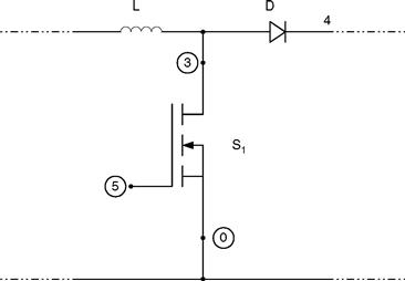
FIGURE 4.27 Example of a power electronic circuit that uses a power MOSFET.
The PSPICE code for the MOS device labeled SI used in Fig. 4.27 is given by,
4.4.5 MOSFET Large-signal Model
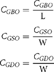
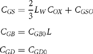
The equivalent circuit of Fig. 4.28 includes five device parasitic capacitances. The capacitors CGB, CGS, CGD, represent the charge-storage effect between the gate terminal and the bulk, source, and drain terminals, respectively. These are non-linear two-terminal capacitors expressed as function of W, L, Cox, VGS, VT0, VDS, and CGBO, CGSO, CGDO, where the capacitors CGBO, CGSO, CGDO are outside the channel region, known as overlap capacitances, that exist between the gate electrode and the other three terminals, respectively. Table 4.1 shows the list of PSPICE MOSFET capacitance parameters and their default values. Notice that the PSPICE overlap capacitors keywords (CGBO, CGSO, CGDO) are proportional either to the MOSFET width or length of the channel as follows:
 (4.46)
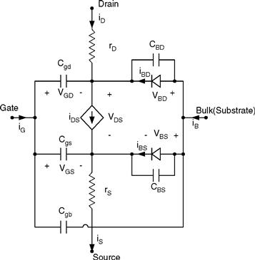
FIGURE 4.28 Large-signal model for the n-channel MOSFET.
In the triode region, vGS > vDS –VTh, the terminal capacitors are given by,
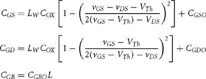 (4.47)
In the saturation (linear) region, we have
 (4.48)
where COX is the per-unit-area oxide capacitance given by,
![]()
KOX = Oxide's relative dielectric constant.
E0 = Free space dielectric constant equals 8.854 × 10− 12 F/m.
TOX = Oxide's thickness layer given as Tox in Table 4.1.
Finally, the diffusion and junction region capacitances between the bulk-to-channel (drain and source) are modeled by CBD and CBS across the two diodes. Because for almost all power MOSFETs, the bulk and source terminals are connected together and at zero potential, diodes DBD and DBS don't have forward bias, resulting in very small conductance values, i.e. small diffusion capacitances. The small-signal model for MOSFET devices is given in Fig. 4.29.
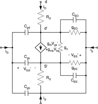
FIGURE 4.29 Small-signal equivalent circuit model for MOSFET.
EXAMPLE 4.4 Figure 4.30a shows an example of a soft switching power factor connection circuit that has two MOSFETs. Its PSPICE simulation waveforms are shown in Fig. 4.30b.
Table 4.2 shows the PSPICE code for Fig. 4.30a.
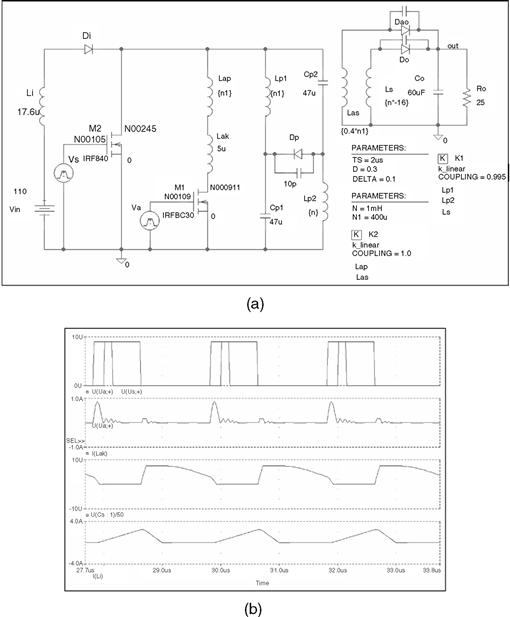
FIGURE 4.30 (a) Example of power electronic circuit and (b) PSPICE simulation waveforms.
TABLE 4.2 PSPICE MOSFET capacitance parameters and their default values for Fig. 4.30a
| * source ZVT-ZCS | |
| D_Do | N00111 OUT Dbreak |
| V_Vs | N00105 0 DC 0 AC 0 PULSE 0 9 0 0 0 {D*Ts} {Ts} |
| L_Ls | 0 N00111 {n*.16} |
| Kn_K1 | L_Lp1 L_Lp2 L_Ls 0.995 |
| C_Co | OUT 0 60uF IC=50 |
| V_Vin | N00103 0 110 |
| L_Li | N00103 N00099 17.6u IC=0 |
| V_Va | N00109 0 DC 0 AC 0 PULSE 0 9 {-Delta*Ts/1.1} 0 0 {2.0*Delta*Ts} |
| {Ts} | |
| D_Dp | N00121 N00169 Dbreak |
| C_C7 | N00111 OUT 30p |
| R_Ro | OUT 0 25 |
| C_C8 | N00143 OUT 10p |
| D_Dao | N00143 OUT Dbreak |
| D_Di | N00099 N00245 Dbreak |
| L_Lp2 | N00121 0 {n} IC=0 |
| C_C9 | N00169 N00121 10p |
| L_Las | N00143 0 {0.4*n1} |
| Kn_K2 | L_Lap L_Las 1.0 |
| L_Lp1 | N00245 N00169 {n} IC=0 |
| L_Lap | N00245 N000791 {n1} |
| C_Cp2 | N00245 N00121 47u IC=170 |
| C_Cp1 | N00169 0 47u IC=170 |
| L_Lak | N000791 N000911 5u IC=0 |
| M_M1 | N000911 N00109 0 0 IRFBC30 |
| M_M2 | N00245 N00105 0 0 IRF840 |
| .PARAM D=0.3 DELTA=0.1 | N1=400u N=1mH TS=2us |
4.4.6 Current MOSFET Performance
The current focus of MOSFET technology development is much more broad than power handling capacity and switching speed; the size, packaging, and cooling of modern MOSFET technology is a major focus. Of course, the development of higher power and efficiency is still paramount, but as modern electronics have become increasingly smaller, the packaging and cooling of power circuits has become more important. It has been indicated by manufacturers that many of their modern MOSFETs are not limited by their semiconductor, but by the packaging. If the MOSFET cannot properly disperse heat, the device will become overheated, which will lead to failure.
An example of modern MOSFET technology is the DirectFET surface mounted MOSFET manufactured by International Rectifier. Part number IRF6662, for example, can handle 47A at 100V, while consuming a board space of 5 × 6 mm, and being only 0.6 mm thick. This switch is efficient at frequencies greater than 1 MHz, and the packaging can dissipate over 50% more heat than traditional surface mounted MOSFETs of similar power ratings. The power density of this switch is many times the power density of similarly rated devices made by International Rectifier in the past. One major factor in the performance gain of this product line is dual-sided cooling. By designing the package to mount to the board through a large contact patch, and by using materials with high heat conductivity, the switch has a very high surface area vs volume ratio, which allows for the heat to be dissipated through the top heat sink as well as through the circuit board.

Another example of manufacturers that are focusing on packaging and cooling to increase the performance of their products is Vishay's PolarPAK and PowerPAK. These devices have a 65% smaller board surface area than traditional SO-8 packages. Also, the thermal conductivity of the package is 88% greater than traditional devices. The PolarPAK device increases the performance by cooling the part from the top and the bottom of the package. These advances in packaging and cooling have allowed the devices to have power densities greater than 250W/mm3 as well, while maintaining high efficiencies into the megahertz.

| **** MOSFET MODEL PARAMETERS | ||
| ********** ******************* *********************** | ||
| IRFBC30 | IRF840 | |
| NMOS | NMOS | |
| LEVEL | 3 | 3 |
| L | 2.000000E-06 | 2.000000E-06 |
| W | .35 | .68 |
| VTO | 3.625 | 3.879 |
| KP | 20.430000E-06 | 20.850000E-06 |
| GAMMA | 0 | 0 |
| PHI | .6 | .6 |
| LAMBDA | 0 | 0 |
| RD | 1.851 | .6703 |
| RS | 5.002000E-03 | 6.382000E-03 |
| RG | 1.052 | .6038 |
| RDS | 2.667000E+ 06 | 2.222000E+ 06 |
| IS | 720.200000E-12 | 56.030000E-12 |
| JS | 0 | 0 |
| PB | .8 | .8 |
| PBSW | .8 | .8 |
| CBD | 790.100000E-12 | 1.415000E-09 |
| CJ | 0 | 0 |
| CJSW | 0 | 0 |
| TT | 685.000000E-09 | 710.000000E-09 |
| CGSO | 1.640000E-09 | 1.625000E-09 |
| CGDO | 123.900000E-12 | 133.400000E-12 |
| CGBO | 0 | 0 |
| TOX | 100.000000E-09 | 100.000000E-09 |
| XJ | 0 | 0 |
| UCRIT | 10.000000E+ 03 | 10.000000E+ 03 |
| DELTA | 0 | 0 |
| ETA | 0 | 0 |
| DIOMOD | 1 | 1 |
| VFB | 0 | 0 |
| LETA | 0 | 0 |
| WETA | 0 | 0 |
| U0 | 0 | 0 |
| TEMP | 0 | 0 |
| VDD | 0 | 0 |
| XPART | 0 | 0 |
Another important characteristic of any solid-state device is the expected service life. For MOSFETs, manufacturers have indicated that the mean time before failure (MTBF) approximately decreases by 50% for every 10°C that the operational temperature increases. For this reason, the current advancement in cooling and packaging has a direct effect on the longevity of the components. While there are definite increases in device longevity every year, the easiest way to have a large impact on the life of the device is to keep the temperature down.
Examples of modern MOSFETs
As development continues, MOSFETs will become smaller, more efficient, higher power density, and higher frequency of operation. As such, MOSFETs will continue to expand into applications that typically use other forms of power switches.
4.5 Future Trends in Power Devices
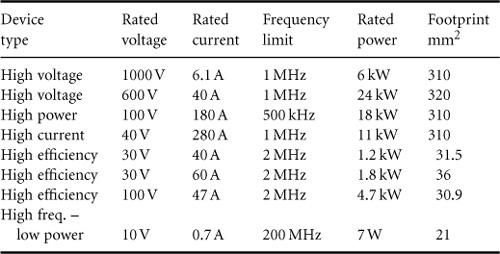
As stated earlier, depending on the applications, the power range processed in power electronic range is very wide, from hundreds of milliwatts to hundreds of megawatts, therefore, it is very difficult to find a single switching device type to cover all power electronic applications. Today's available power devices have tremendous power and frequency rating range as well as diversity. Their forward current ratings range from a few amperes to a few kiloamperes, blocking voltage rating ranges from a few volts to a few of kilovolts, and switching frequency ranges from a few hundred of hertz to a few megahertz as illustrated in Table 4.3. This table illustrates the relative comparison between available power semiconductor devices. We only give relative comparison because there is no straightforward technique that gives ranking of these devices. As we accumulate this table, devices are still being developed very rapidly with higher current, voltage ratings, and switching frequency.
TABLE 4.3 Comparison of power semiconductor devices
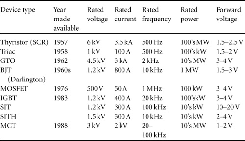
It is expected that improvement in power handling capabilities and increasing frequency of operation of power devices will continue to drive the research and development in semiconductor technology. From power MOSFET to power MOS-IGBT and to power MOS-controlled thyristors, power rating has consistently increased by a factor of 5 from one type to another. Major research activities will focus on obtaining new device structure based on MOS-BJT technology integration to rapidly increase power ratings. It is expected that the power MOS-BJT technology will capture more than 90% of the total power transistor market.
The continuing development of power semiconductor technology has resulted in power systems with driver circuit, logic and control, device protection, and switching devices being designed and fabricated on a single-chip. Such power IC modules are called “smart power” devices. For example, some of today's power supplies are available as IC's for use in low-power applications. No doubt the development of smart power devices will continue in the near future, addressing more power electronic applications.
REFERENCES
1. Jayant Baliga B. Power Semiconductor Devices. 1996.
2. Lorenz L, Marz M, Amann H. Rugged Power MOSFET- A milestone on the road to a simplified circuit engineering. SIEMENS application notes on S-FET application. 1998.
3. Rashid M. Microelectronics. Thomson-Engineering 1998.
4. Sedra, Smith. Microelectronic Circuits. 4th Edition Oxford Series 1996.
5. Ned Mohan, Underland, Robbins. Power Electronics: Converters, Applications and Design. 2nd Edition John Wiley 1995.
6. Cobbold R. Theory and Applications of Field Effect Transistor. John Wiley 1970.
7. Warner RM, Grung BL. MOSFET: Theory and Design. Oxford 1999.
8. Power FET’s and Their Application. Prentice-Hall 1982.
9. Gottling JG. Hands on pspice. Houghton Mifflin Company 1995.
10. Massobrio G, Antognetti P. Semiconductor Device Modeling with PSPICE. McGraw-Hill 1993.