
9
Static Induction Devices
Alabama Microelectronics Science and Technology Center, Auburn University, Alabama, USA
9.1 Introduction
9.2 Theory of Static Induction Devices
9.3 Characteristics of Static Induction Transistor
9.4 Bipolar Mode Operation of SI devices (BSIT)
9.5 CMT Conductivity Modulation Transistor
9.7 Lateral Punch-Through Transistor
9.8 Static Induction Transistor Logic
9.9 BIT Saturation Protected by SIT
9.10 Static Induction MOS Transistor
9.11 Space Charge Limiting Load (SCLL)
9.13 Static Induction Thyristor
9.15 Summary
9.1 Introduction
Static induction devices were invented in 1975 by J. Nishizawa [1], and for many years, lapan was the only country where static induction family devices were successfully fabricated. Static induction transistor can be considered a short channel junction field effect transistor (JFET) device operating in prepunch-through region. The number of devices in this family is increasing with time. The SIT can operate with power more than 100 kW at 100 kHz and more than 150 W at 3 GHz [2]. These devices may operate up to THz frequencies [3, 4]. Static induction transistor logic had switching energy 100 times smaller than its I2 L competitor [5,6]. Static induction thyristor has many advantages over the traditional silicon controlled rectifier (SCR), and SID exhibits high switching speed, large reverse voltage, and low forward voltage drops [7].
9.2 Theory of Static Induction Devices
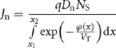
The cross section of the SIT is shown in Fig. 9.1 and its characteristics are shown in Fig. 9.2. An induced electrostatically potential barrier controls the current in static induction devices. The derivations of formulas will be done for an n-channel device, but the obtained results with a little modification can also be applied to p-channel devices. For a small electrical field existing in the vicinity of the potential barrier, the drift and diffusion currents can be approximated by
![]() (9.1)
(9.1)
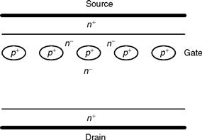
FIGURE 9.1 Cross section of the static induction transistor.
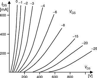
FIGURE 9.2 Characteristics of the early SIT design [1].
where Dn = μn VT and VT = kT/q. By multiplying both sides of the equation by exp(− ϕ(x)/VT) and rearranging
![]() (9.2)
(9.2)
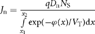
By integrating from x1 to x2, one can obtain
 (9.3)
(9.3)
With the following boundary conditions
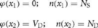 (9.4)
(9.4)
Equation (9.3) reduces to
 (9.5)
(9.5)
Note that the above equations derived for SIT can also be used to find the current in any device controlled by a potential barrier, such as a bipolar transistor, an MOS transistor operating in subthreshold mode, or in a Schottky diode.
9.3 Characteristics of Static Induction Transistor
Samples of the potential distribution in the SI devices are shown in Fig. 9.3 [7]. The vicinity of the potential barrier can be approximated using parabolic formulas (Fig. 9.4) along and across the channel [8, 9].

FIGURE 9.3 Potential distribution in SIT: (a) view from the source side and (b) view from the drain side.
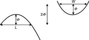
FIGURE 9.4 Potential distribution in the vicinity of the barrier approximated by parabolic shapes.
![]() (9.6)
(9.6)
Integrating Eq. (9.5) first along the channel and then across the channel yields a very simple formula for drain currents in n-channel SITs:
![]() (9.8)
(9.8)
where Φ is the potential barrier height in reference to the source potential, NS is the electron concentration at the source, W/L ratio describes the shape of the potential saddle in the vicinity of the barrier, and Z is the length of the source strip.
Since barrier height F can be a linear function of gate and drain voltages, therefore
![]() (9.9)
(9.9)
The above equation describes characteristics of SIT for small current levels. For large current levels, the device current is controlled by the space charge of moving carriers. In one-dimensional case, the potential distribution is described by the Poisson equation:
![]() (9.10)
(9.10)
where A is the effective device cross section and v(x) is the carrier velocity. For a small electrical field v(x) = μ(x), Eq. (9.10) results in
![]() (9.11)
(9.11)
and for a large electrical field v(x) = const, Eq. (9.10) results in
![]() (9.12)
(9.12)
where L is the channel length and vsat ≈ 1011 μm/s is the carrier saturation velocity. In practical devices, the current-voltage relationship is described by an exponential relationship, Eq. (9.9), for small currents by a quadratic relationship, Eq. (9.11), and finally for large voltages by an almost linear relationship, Eq. (9.12). Static induction transistor characteristics drawn in linear and logarithmic scales are shown in Figs. 9.5 and 9.6, respectively.
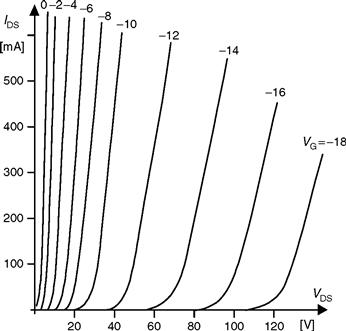
FIGURE 9.5 Characteristics of the SIT drawn in a linear scale.
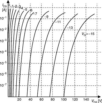
FIGURE 9.6 Characteristics of the SIT drawn in a logarithmic scale.
9.4 Bipolar Mode Operation of SI devices (BSIT)
The bipolar mode of operation of an SIT was first reported in 1976 by Nishizawa and Wilamowski [5, 6]. Several complex theories for the bipolar mode of operation were developed [10–14], but actually the simple formula given by Eq. (9.5) works well not only for the typical mode of the SIT operation but also for the bipolar mode of the SIT operation. Furthermore, the same formula works very well for the classical bipolar transistors. Typical characteristics of the SIT operating in normal and bipolar modes are shown in Figs. 9.7 and 9.8.
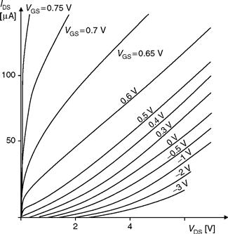
FIGURE 9.7 Small-size SIT characteristics operating in both the normal and bipolar modes, ID = f(VDS) with VGS as a parameter.
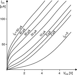
FIGURE 9.8 Small-size SIT characteristics, operating in both the normal and bipolar modes, ID = f (VDS) with IG as a parameter.
A potential barrier controls the current in the SIT, as shown in Fig. 9.9 and it is given by
 (9.13)
where ϕ(x) is the profile of the potential barrier along the channel.
FIGURE 9.9 Potential distributions in SIT: (a) traditional and (b) with sharp potential barrier.
For example, in the case of npn bipolar transistors, the potential distribution across the base in reference to emitter potential at the reference impurity level NE = NS is described by
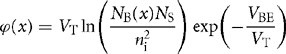 (9.14)
After substituting Eq. (9.14) into Eq. (9.13), one can obtain the well-known equation for electron current injected into the base
![]() (9.15)
(9.15)
If Eq. (9.13) is valid for SIT and BJT, then one may assume that it is also valid for the bipolar mode of operation of the SIT transistor. This is a well-known equation for the collector current in the bipolar transistor, but this time it was derived using the concept of the current flow through the potential barrier.
9.5 CMT Conductivity Modulation Transistor
The CMT conductivity modulation transistor has a unique ability of controlling ac current flow without a significant distortion of the sinusoidal waveforms of flowing current [15]. The principle of operation of the CMT is illustrated in Fig. 9.10. The potential profile of an n+n−n+ structure is shown in Fig. 9.10a. One may notice that holes injected in the n− region will drift to the lowest potential and will be trapped near a potential barrier. In the case of forward direction, holes would be in vicinity of the base B1, and in the case of reverse bias, holes would be in the base B2. The positive charge of trapped holes would lower the potential barriers near source or drain depending on the direction of applied voltages. As a consequence, larger current may flow through lowered potential barrier.
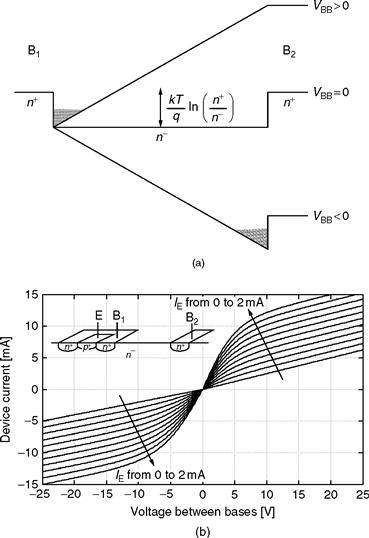
FIGURE 9.10 CMT conductivity modulation transistor: (a) band diagrams and (b) typical current-voltage characteristics.
In either biasing configuration, holes are trapped by the potential well, and the number of accumulated holes in the vicinity of the potential barrier will depend upon the local recombination rate. The voltage drop across a region of hole accumulation is quite small due to the effect of conductivity modulation. In this manner, the device operation is relatively independent of the electric polarity between B1 and B2.
The device has the unique characteristics of allowing for proper operation for both polarities of B1-B2 base voltages while the controlling emitter current direction remains unchanged (see Fig. 9.10b). Also, it should be noted that in the vicinity of zero biasing, the device has extremely linear characteristics. In fact, it behaves as a variable resistor controlled by current injected by the emitter.
9.6 Static Induction Diode
The bipolar mode of operation of the SIT can also be used to obtain diodes with low forward voltage drop and negligible carrier storage effect [10, 11, 13, 16]. A static induction diode (SID) can be obtained by shorting a gate to the emitter of the SIT [17, 18]. Such diode has all the advantages of the SIT such as thermal stability and short switching time. The cross section of such diode is shown in Fig. 9.11.
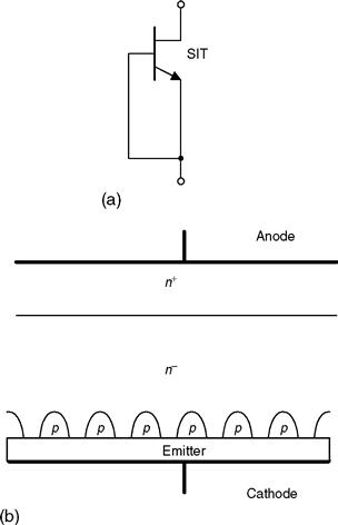
FIGURE 9.11 Static induction diode: (a) circuit diagram and (b) cross section.
The quality of the SID can be further improved with more sophisticated emitters (Fig. 9.10b,c). The SI diode with Schottky emitter was described by Wilamowski in 1983 [19] (Fig. 9.12). A similar structure was later published by Baliga [20].
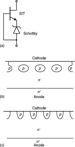
FIGURE 9.12 Schottky diode with enlarged breakdown voltages: (a) circuit diagram, (b) and (c) two cross sections of possible implementation.
9.7 Lateral Punch-Through Transistor
Fabrications of SI transistors usually require very sophisticated technology. It is much simpler to fabricate a lateral punch-through transistor, which operates on the same principle and has similar characteristics [21] (Fig. 9.13). The cross section of the LPTT is shown in Fig. 9.14.
FIGURE 9.13 Characteristics of lateral punch-through transistor.

FIGURE 9.14 Structures of the lateral punch-through transistors: (a) simple and (b) with sharper potential barrier.
9.8 Static Induction Transistor Logic
The static induction transistor logic (SITL) was proposed by Nishizawa and Wilamowski [5,6]. This logic circuit has almost 100 times better power-delay product than its I2 L competitor. Such drastic improvement of the power-delay product is possible because the SITL structure has a significantly smaller junction parasitic capacitance, and also the voltage swing is reduced. Figures 9.15 and 9.16 illustrate the concept of SITL. Measured characteristics of an n-channel transistor of the static induction logic are shown in Fig. 9.17.
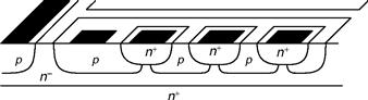
FIGURE 9.15 Cross section of SIT logic.
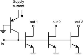
FIGURE 9.16 Diagrams of SIT logic.
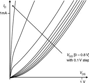
FIGURE 9.17 Measured characteristics of n-channel transistor of the logic circuit of Fig. 9.16.
9.9 BJT Saturation Protected by SIT
The SI transistor can also be used instead of a Schottky diode to protect a bipolar junction transistor against saturation [22]. This leads to faster switching time. The concept is shown in Figs. 9.18 and 9.19. Note that this approach is advantageous to the solution with Schottky diode since it does not require additional area on a chip and it does not introduce additional capacitance between the base and the collector. The base collector capacitance is always enlarged by the Miller effect, and this leads to slower switching in the case of the solution with the Schottky diode.
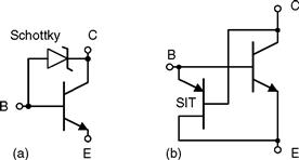
FIGURE 9.18 Protection of bipolar transistor against deep saturation: (a) using Schottky diode and (b) using SIT.
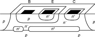
FIGURE 9.19 Cross sections of bipolar transistors protected against deep saturation using SIT.
9.10 Static Induction MOS Transistor
The punch-through transistor with MOS-controlled gate was described in 1983 [23, 24]. In the illustration shown inFig. 9.20a, current can flow in a similar fashion as in the lateral punch-through transistor [21]. In this mode of operation, carriers are moving far from the surface with a velocity close to the saturation velocity. The real advantage of such structure is the very low gate capacitance.
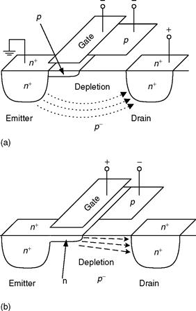
FIGURE 9.20 MOS controlled punch-through transistor: (a) transistor in the punch-through mode for the negative gate potential and (b) transistor in the on-state for the positive gate potential.
Another implementation of static induction MOS transistor (SIMOS) is shown in Fig. 9.21. The buried p+ layer is connected to the substrate, which has a large negative potential. As a result, the potential barrier is high and the emitter–drain current cannot flow. The punch-through current may start to flow when the positive voltage is applied to the gate, and hence in this way, the potential barrier is lowered. The p-implant layer is depleted, and due to the high horizontal electrical field under the gate, there is no charge accumulation under this gate. Such a transistor has several advantages over the traditional MOS transistor.
1. The gate capacitance is very small, since there is no accumulation layer under the gate.
2. Carriers are moving with a velocity close to saturation velocity.
3. Much lower substrate doping and the existing depletion layer lead to much smaller drain capacitance.
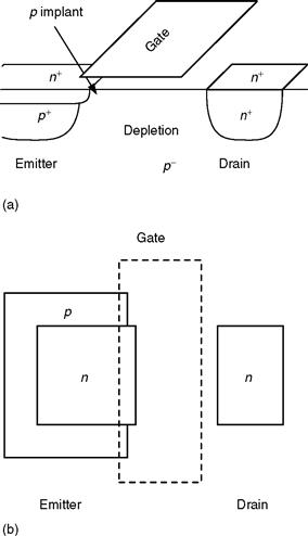
FIGURE 9.21 Static induction MOS structure: (a) cross section and (b) top view.
The device operates in a similar fashion as MOS transistor in subthreshold conditions, but this process occurs at much higher current levels. Such “bipolar mode” of operation may have many advantages in VLSI applications.
9.11 Space Charge Limiting Load (SCLL)
Using the concept of the space charge limited current flow, as shown in Fig. 9.22, it is possible to fabricate very large resistors on a very small area. Moreover, these resistors have a very small parasitic capacitance. For example, a 50-kω resistor requires only several square micrometers when 2-μm feature size technology is used [7].
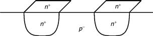
FIGURE 9.22 Space charge limiting load (SCLL).
Depending on the value of the electrical field, the device current is described by the following two equations. For a small electrical field v(x) = μE(x)
 (9.16)
For a large electrical field v(x) = const
![]() (9.17)
(9.17)
Moreover, these resistors, which are based on the space charge limit flow, have a very small parasitic capacitance.
9.12 Power MOS Transistors
Power MOS transistors are being used for fast switching power supplies and for switching power converters. They can be driven with relatively small power, and switching frequencies could be very high. High switching frequencies lead to compact circuit implementations with small inductors and small capacitances. Basically, only two technologies, DMOS and VMOS, are used for power MOS devices as shown in Figs. 9.23 and 9.24.
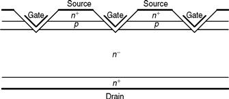
FIGURE 9.23 Cross section of the VMOS transistor.
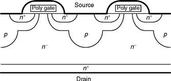
FIGURE 9.24 Cross section of the DMOS transistor.
A more popular structure is the DMOS shown in Fig. 9.24. This structure also uses the SIT concept. Note that for large drain voltages, the n-region is depleted from carriers and statically induced electrical field in the vicinity of the virtual drain is significantly reduced. As a result, this transistor may withstand much larger drain voltages and also the effect of channel length modulation is significantly reduced. The later effect leads to larger output resistances of the transistor. Therefore, the drain current is less sensitive to drain voltage variations. The structure shown in Fig. 9.24 can be considered a composition of the MOS transistor and the SIT transistor as shown in Fig. 9.25.
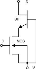
FIGURE 9.25 MOS and SIT equivalent to the structure of Fig. 9.24.
The major disadvantage of power MOS transistors is relatively large drain series resistance and much smaller transconductance in comparison to bipolar transistors. Both of these parameters can be improved dramatically by a simple change of the type of drain, in the case of n-channel device from n-type to p-type drain. This way the integrated structure is being built where its equivalent diagram consists of MOS transistor integrated with bipolar transistor. Such structure has times larger transconductance (is the current gain of bipolar transistor) and much smaller series resistance due to the conductivity modulation effect caused by holes injected into lightly doped drain region. Such device is known as insulated gate bipolar transistors (IGBT), which is shown in Fig. 9.26. Their main disadvantage is large switching time limited primarily by poor switching performance of bipolar transistor. Another difficulty is related to a possible latch-up action of four-layer n+pn−p+ structure. This undesired effect could be suppressed by using heavily doped p+ region in the base of NPN structure, which leads to significant reduction of the current gain of this parasitic transistor. The gain of other PNP transistor must be kept large, so the transconductance of the entire device is large too. The IGBT transistor has breakdown voltages up to 1500 V, and turn-off times are in the range 0.1-0.5μs. They may operate with currents above 100 A with a forward voltage drop of about 3 V.
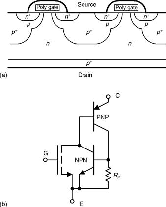
FIGURE 9.26 Insulated gate bipolar transistor (IGBT): (a) cross section and (b) equivalent diagram.
9.13 Static Induction Thyristor
There are several special semiconductor devices dedicated to high-power applications. The most popular is thyristor known also as silicon control rectifier (SCR). This device is a four-layer structure as shown in Fig. 9.27a and it can be considered as two transistors npn and pnp connected as shown in Fig. 9.27b.
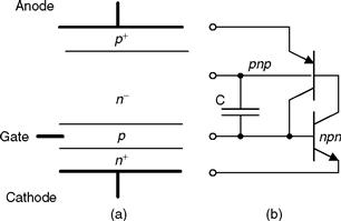
FIGURE 9.27 Silicon control rectifier: (a) cross section and (b) equivalent diagram.
In normal operation mode (anode has positive potential), only one junction is reverse-biased, and it can be represented by capacitance C. A spike of anode voltage can, therefore, be obtained through capacitor C, and it can trigger SCR. This behavior is not acceptable in practical applications and therefore a different device structure is being used as shown in Fig. 9.28. Note that by shorting gate to cathode by resistor R, it is much more difficult to trigger the npn transistor by spike of anode voltage. This way rapid change of anode voltages is not able to trigger thyristor. Therefore, this structure has very large dv/dt parameter.
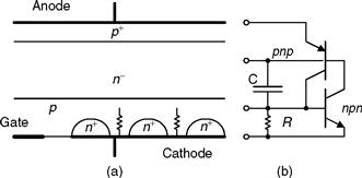
FIGURE 9.28 Silicon control rectifier with larger dv/dt parameter: (a) cross section and (b) equivalent diagram.
When NPN transistor is replaced with SItransistor, parameters of a thyristor can be significantly improved. For example, with breaking voltage in the range of 5 kV and current of 600 A, the switching on time can be as short as 100 ns and dv/dt parameter can be as large as 50 kV/s [16, 25].
Most of the SCRs sold in the market comprise an integrated structure composed of two or more thyristors. This structure has both large dv/dt and di/dt parameters. This structure consists of internal thyristor that significantly amplifies the gate signal.
The classical thyristor shown in Fig. 9.27 can be turned off by the gate voltage while integrated SCR shown in Fig. 9.29 can be only turned off by decreasing anode current to zero. Most of the SCRs sold in the market have an integrated structure composed of two or more thyristors. This structure has both large dv/dt and di/dt parameters.
FIGURE 9.29 Integrated structure of silicon control rectifier: (a) cross section and (b) equivalent diagram.
9.14 Gate Turn-Off Thyristor
For dc operation, it is important to have a thyristor that can be turned off by the gate voltage. Such thyristor has a structure similar to the one shown in Fig. 9.27. However, it is important to have significantly different current gains β for pnp and npn transistors. The current gain of npn transistor should be as large as possible, and the current gain of pnp transistor should be small. The product of βnpn and βpnp should be larger than one. This can be easily implemented using SI structure as shown in Fig. 9.30.
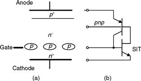
FIGURE 9.30 GTO-SIT: (a) cross section and (b) equivalent diagram.
9.15 Summary
Several devices from the static induction family such as static induction transistor (SIT), static induction diode (SID), static induction thyristor, lateral punch-through transistor (LPTT), static induction transistor logic (SITL), static induction MOS transistor (SIMOS), and space charge limiting load (SCLL) are described. The theory of operation of static induction devices is given for both a current controlled by a potential barrier and a current controlled by space charge. The new concept of a punch-through emitter (PTE), which operates with majority carrier transport, is presented.
REFERENCES
1. Nishizawa J, Terasaki T, Shibata J. Field-Effect Transistor versus Analog Transistor (Static Induction Transistor). IEEE Trans. Electron Devices. April 1975; vol. 22(No. 4):185–197.
2. Tatsude M, Yamanaka E, Nishizawa J. High-Frequency High-Power Static Induction Transistor. IEEE Industry Application Magazine. March/April 1995; vol. 1(No. 2):40–45.
3. Nishizawa J, Plotka P, Kurabayashi T. Ballistic and Tunneling GaAs Static Induction Transistors: Nano-Devices for THz Electronics. IEEE Trans. Electron Devices. 2002; vol. 49(No. 7):1102–1111.
4. Nishizawa J, Suto K, Kurabayashi T. Recent Advance in Tetrahertz Wave and Material Basis. Russian Physics Journal. 2003; vol. 46(No. 6):615–622.
5. Nishizawa J, Wilamowski BM. Integrated Logic –State Induction Transistor Logic. In: International Solid State Circuit Conf.. Philadelphia USA 1977. [pp. 222–223].
6. Nishizawa J, Wilamowski BM. Static Induction Logic –A Simple Structure with Very Low Switching Energy and Very High Packing Density. In: Int. Con. Solid State Devices. 1976 1977. [pp. 53–54] Journal of Japanese Society of Applied Physics. 1976 1977; vol. 16(No. 1):158–162.
7. Wilamowski BM. High Speed, High Voltage, and Energy Efficient Static Induction Devices. In: 12 Symposium of Static Induction Devices –SSID’ 99. 1999: 23–28.
8. Plotka P, Wilamowski BM. Interpretation of Exponential Type Drain Characteristics of the SIT. Solid-State Electronics. 1980; vol. 23:693–694.
9. Plotka P, Wilamowski BM. Temperature Properties of the Static Induction Transistor. Solid-State Electronics. 1981; vol. 24:105–107.
10. Kim CW, Kimura M, Yano K, Tanaka A, Sukegawa T. Bipolar-Mode Static Induction Transistor: Experiment and Two-Dimensional Analysis. IEEE Trans. Electron Devices. September 1990; vol. 37(No. 9):2070–2075.
11. Nakamura Y, Tadano H, Takigawa M, Igarashi I, Nishizawa J. Experimental Study on Current Gain of BSIT. IEEE Trans. Electron Devices. June 1986; vol. 33(No. 6):810–815.
12. Nishizawa J, Ohmi T, Chen HL. Analysis of Static Characteristics of a Bipolar-Mode SIT (BSIT). IEEE Trans. Electron Devices. August 1982; vol. 29(No. 8):1233–1244.
13. Yano K, Henmi I, Kasuga M, Shimizu A. High-Power Rectifier Using the BSIT Operation. IEEE Trans. Electron Devices. February 1998; vol. 45(No. 2):563–565.
14. Yano K, Masahito M, Moroshima H, Morita J, Kasuga M, Shimizu A. Rectifier Characteristics Based on Bipolar-Mode SIT Operation. IEEE Electron Device Letters. September 1994; vol. 15(No. 9):321–323.
15. Wilamowski BM, Englert TJ. CMT - Conductivity-Modulated Transistor”. IEEE Trans. Electron Devices. 1992; vol. 39:2600–2606.
16. Hironaka R, Watanabe M, Hotta E, Okino A. Performance of Pulsed Power Generator using High Voltage Static Induction Thyristor. IEEE Trans. Plasma Science. 2000; vol. 28(No. 5):1524–1527.
17. Yano K, Honarkhah S, Salama A. Lateral SOI Static Induction Rectifiers. In: Proc. Int. Symp. Power Semiconductor Devices. Osaka 2001. [pp. 247–250].
18. Yano K, Hattori N, Yamamoto Y, Kasuga M. Impacts of Channel Implantation on Performance of Static Shielding Diodes and Static Induction Rectifiers. In: Proc. Int. Symp. Power Semiconductor Devices. Osaka 2001. [pp. 219–222].
19. Wilamowski BM. Schottky Diodes with High Breakdown voltage. Solid-State Electronics. 1983; vol. 26(No. 5):491–493.
20. Baliga BJ. The Pinch Rectifier: A Low Forward-Drop, High-Speed Power Diode. IEEE Electron Device Letters. 1984; vol. 5:194–196.
21. Wilamowski BM, Jaeger RC. The Lateral Punch-Through Transistor. IEEE Electron Device Letters. 1982; vol. 3(No. 10):277–280.
22. Wilamowski BM, Mattson RH, Staszak ZJ. The SIT saturation protected bipolar transistor. IEEE Electron Device Letters. 1984; vol. 5:263–265.
23. Wilamowski BM. The Punch-Through Transistor with MOS Controlled Gate. Physica Status Solidi (a). 1983; vol. 79:631–637.
24. Wilamowski BM, Jaeger RC, Fordemwalt JN. Buried MOS Transistor with Punch-Through. Solid State Electronics. 1984; vol. 27(No. 8/9):811–815.
25. Shimizu N, Sekiya T, Iida K, Imanishi Y, Kimura M, Nishizawa J. Over 55kV/us, dv/dt turnoff characteristics of 4kV-Static Induction Thyristor for Pulsed Power Applications. In: Proc. Int. Symp. Power Semiconductor Devices. 2004. [pp. 281–284].