
11
Single-phase Controlled Rectifiers
Pablo Lezana, Samir Kouro, and Alejandro Weinstein Department of Electronics, Universidad Técnica Federico Santa María, Valparaíso, Chile
11.1 Introduction
11.2 Line-commutated Single-phase Controlled Rectifiers
11.2.1 Single-phase Half-wave Rectifier
11.2.2 Bi-phase Half-wave Rectifier
11.2.3 Single-phase Bridge Rectifier
11.2.4 Analysis of the Input Current
11.2.5 Power Factor of the Rectifier
11.2.6 The Commutation of the Thyristors
11.2.7 Operation in the Inverting Mode
11.2.8 Applications
11.1 Introduction
This chapter is dedicated to single-phase controlled rectifiers, which are used in a wide range of applications. As shown in Fig. 11.1, single-phase rectifiers can be classified into two big categories:
(i) Topologies working with low switching frequency, also known as line commutated or phase controlled rectifiers.
(ii) Circuits working with high switching frequency, also known as power factor correctors (PFCs).
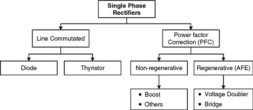
FIGURE 11.1 Single-phase rectifier classification.
Line-commutated rectifiers with diodes, covered in a previous chapter of this handbook, do not allow the control of power being converted from ac to dc. This control can be achieved with the use of thyristors. These controlled rectifiers are addressed in the first part of this chapter.
In the last years, increasing attention has been paid to the control of current harmonics present at the input side of the rectifiers, originating from a very important development in the so-called PFC. These circuits use power transistors working with high switching frequency to improve the waveform quality of the input current, increasing the power factor. High power factor rectifiers can be classified in regenerative and non-regenerative topologies and they are covered in the second part of this chapter.
11.2 Line-commutated Single-phase Controlled Rectifiers
11.2.1 Single-phase Half-wave Rectifier
The single-phase half-wave rectifier uses a single thyristor to control the load voltage as shown in Fig. 11.2. The thyristor will conduct, on-state, when the voltage vT is positive and a firing current pulse iG is applied to the gate terminal. The control of the load voltage is performed by delaying the firing pulse by an angle α. The firing angle α is measured from the position where a diode would naturally conduct. In case of Fig. 11.2 the angle α is measured from the zero-crossing point of the supply voltage vs. The load in Fig. 11.2 is resistive and therefore the current id has the same waveform of the load voltage. The thyristor goes to the non-conducting condition, off-state, when the load voltage, and consequently the current, reaches a negative value.
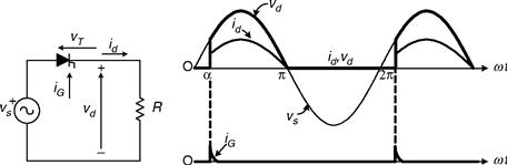
FIGURE 11.2 Single-thyristor rectifier with resistive load.
The load average voltage is given by
![]() (11.1)
(11.1)
where Vmax is the supply peak voltage. Hence, it can be seen from Eq. (11.1) that changing the firing angle α controls both the load average voltage and the amount of transferred power.
Figure 11.3a shows the rectifier waveforms for an R–L load. When the thyristor is turned on, the voltage across the inductance is
![]() (11.2)
(11.2)
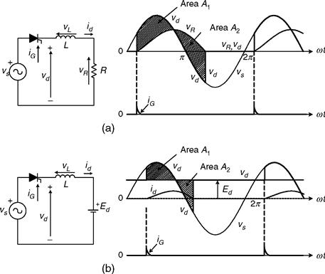
FIGURE 11.3 Single-thyristor rectifier with: (a) resistive-inductive load and (b) active load.
where VR is the voltage in the resistance R, given by VR = R.id. If vs - VR > 0, from Eq. (11.2) holds that the load current increases its value. On the other hand, id decreases its value when vs- VR < 0. The load current is given by
![]() (11.3)
(11.3)
Graphically, Eq. (11.3) means that the load current id is equal to zero when A1 = A2, maintaining the thyristor in conduction state even when vs < 0.
When an inductive–active load is connected to the rectifier, as illustrated in Fig. 11.3b, the thyristor will be turned on if the firing pulse is applied to the gate when vs > Ed. Again, the thyristor will remain in the on-state until A1 = A2. When the thyristor is turned off, the load voltage will be vd = Ed.
11.2.2 Bi-phase Half-wave Rectifier
The bi-phase half-wave rectifier, shown in Fig. 11.4, uses a center-tapped transformer to provide two voltages v1 and v2. These two voltages are 180° out of phase with respect to the mid-point neutral N. In this scheme, the load is fed via thyristors T1 and T2 during each positive cycle of voltages v1 and v2, respectively, while the load current returns via the neutral N.
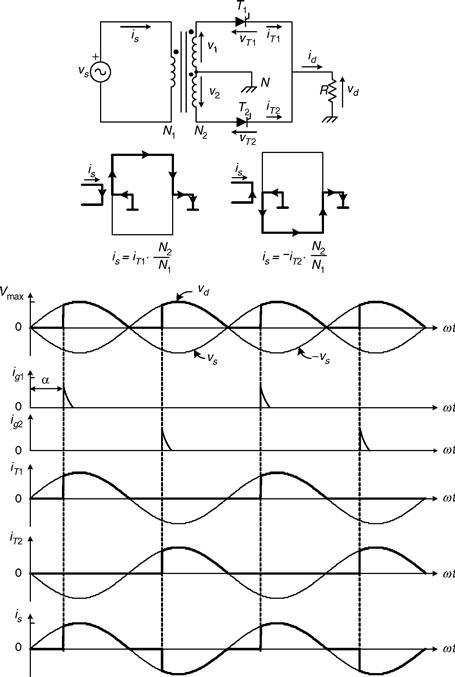
FIGURE 11.4 Bi-phase half-wave rectifier.
As illustrated in Fig. 11.4, thyristor T1 can be fired into the on-state at any time while voltage vT1 > 0. The firing pulses are delayed by an angle α with respect to the instant where diodes would conduct. Also the current paths for each conduction state are presented in Fig. 11.4. Thyristor T1 remains in the on-state until the load current tends to a negative value. Thyristor T2 is fired into the on-state when vT2 > 0, which corresponds in Fig. 11.4 to the condition when v2 > 0.
The mean value of the load voltage with resistive load is determined by
![]() (11.4)
(11.4)
The ac supply current is equal to iT1 (N2 /N1) when T1 is in the on-state and –iT2(N2/N1) when T2 is in the on-state, where N2 /N1 is the transformer turns ratio.
The effect of the load time constant TL, = L/R, on the normalized load current id(t)/îR(t) for a firing angle α = 0° is shown in Fig. 11.5. The ripple in the load current reduces as the load inductance increases. If the load inductance L → ∞ then the current is perfectly filtered.
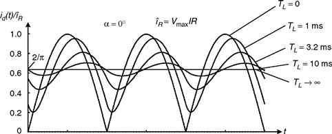
FIGURE 11.5 Effect of the load time constant over the current ripple.
11.2.3 Single-phase Bridge Rectifier
Figure 11.6a shows a fully controlled bridge rectifier, which uses four thyristors to control the average load voltage. In addition, Fig. 11.6b shows the half-controlled bridge rectifier which uses two thyristors and two diodes.

FIGURE 11.6 Single-phase bridge rectifier: (a) fully controlled and (b) half-controlled.
The voltage and current waveforms of the fully controlled bridge rectifier for a resistive load are illustrated in Fig 11.7. Thyristors T1 and T2 must be fired on simultaneously during the positive half-wave of the source voltage vs, to allow the conduction of current. Alternatively, thyristors T3 and T4 must be fired simultaneously during the negative half-wave of the source voltage. To ensure simultaneous firing, thyristors T1 and T2 use the same firing signal. The load voltage is similar to the voltage obtained with the bi-phase half-wave rectifier. The input current is given by
![]() (11.5)
(11.5)
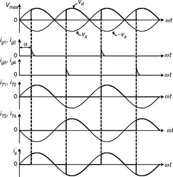
FIGURE 11.7 Waveforms of a fully controlled bridge rectifier with resistive load.
and its waveform is shown in Fig. 11.7.
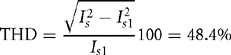
Figure 11.8 presents the behavior of the fully controlled rectifier with resistive-inductive load (with L → ∞). The high load inductance generates a perfectly filtered current and the rectifier behaves like a current source. With continuous load current, thyristors T1 and T2 remain in the on-state beyond the positive half-wave of the source voltage vs. For this reason, the load voltage vd can have a negative instantaneous value. The firing of thyristors T3 and T4 has two effects:
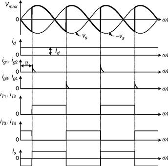
FIGURE 11.8 Waveforms of a fully controlled bridge rectifier with resistive-inductive load (L → ∞).
This is the main reason why this type of converters are called “naturally commutated” or “line commutated” rectifiers. The supply current iS has the square waveform, as shown in Fig. 11.9, for continuous conduction. In this case, the average load voltage is given by
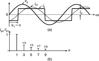
FIGURE 11.9 Input current of the single-phase controlled rectifier in bridge connection: (a) waveforms and (b) harmonics spectrum.
![]() (11.6)
(11.6)
11.2.4 Analysis of the Input Current
Considering a very high inductive load, the input current in a bridge-controlled rectifier is filtered and presents a square waveform. In addition, the input current is is shifted by the firing angle α with respect to the input voltage vs, as shown in Fig. 11.9a. The input current can be expressed as a Fourier series, where the amplitude of the different harmonics are
![]() (11.7)
(11.7)
where n is the harmonic order. The root mean square (rms) value of each harmonic can be expressed as
![]() (11.8)
(11.8)
Thus, the rms value of the fundamental current is1 is
![]() (11.9)
(11.9)
It can be observed from Fig. 11.9a that the displacement angle ϕ1 of the fundamental current is1 corresponds to the firing angle α Figure 11.9b shows that in the harmonic spectrum of the input current, only odd harmonics are present with decreasing amplitude while the frequency increases. Finally the rms value of the input current is is
![]() (11.10)
(11.10)
The total harmonic distortion (THD) of the input current can be determined by
 (11.11)
11.2.5 Power Factor of the Rectifier
The displacement factor of the fundamental current, obtained from Fig. 11.9a is
![]() (11.12)
(11.12)
In the case of non-sinusoidal currents, the active power delivered by the sinusoidal single-phase supply is
![]() (11.13)
(11.13)
where Vs is the rms value of the single-phase voltage vs. The apparent power is given by
![]() (11.14)
(11.14)
The power factor (PF) is defined by
![]() (11.15)
(11.15)
Substitution from Eqs. (11.12), (11.13), and (11.14) in Eq. (11.15) yields
![]() (11.16)
(11.16)
This equation shows clearly that due to the non-sinusoidal waveform of the input current, the power factor of the rectifier is negatively affected both by the firing angle α and by the distortion of the input current. In effect, an increase in the distortion of the current produces an increase in the value of Is in Eq. (11.16), which deteriorates the power factor.
11.2.6 The Commutation of the Thyristors
Until now, the current commutation between thyristors has been considered to be instantaneous. This condition is not valid in real cases due to the presence of the line inductance L, as shown in Fig. 11.10a. During the commutation, the current through the thyristors cannot change instantaneously, and for this reason, during the commutation angle μ, all four thyristors are conducting simultaneously. Therefore, during the commutation, the following relationship for the load voltage holds
![]() (11.17)
(11.17)
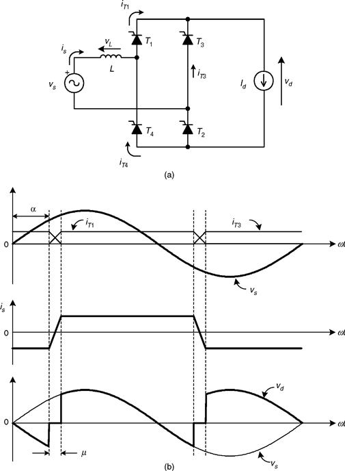
FIGURE 11.10 The commutation process: (a) circuit and (b) waveforms.
The effect of the commutation on the supply current, voltage waveforms, and the thyristor current waveforms can be observed in Fig. 11.10b.
During the commutation, the following expression holds
![]() (11.18)
(11.18)
Integrating Eq. (11.18) over the commutation interval yields
![]() (11.19)
(11.19)
From Eq. (11.19), the following relationship for the commutation angle μ is obtained
![]() (11.20)
(11.20)
Equation (11.20) shows that an increase of the line inductance L or an increase of the load current Id increases the commutation angle μ. In addition, the commutation angle is affected by the firing angle α In effect, Eq. (11.18) shows that with different values of α the supply voltage vs has a different instantaneous value, which produces different dis/dt, thereby affecting the duration of the commutation.
Equation (11.17) and the waveform of Fig. 11.10b show that the commutation process reduces the average load voltage Vdα. When the commutation is considered, the expression for the average load voltage is given by
![]() (11.21)
(11.21)
Substituting Eq. (11.20) into Eq. (11.21) yields
![]() (11.22)
(11.22)
11.2.7 Operation in the Inverting Mode
When the angle α > 90°, it is possible to obtain a negative average load voltage. In this condition, the power is fed back to the single-phase supply from the load. This operating mode is called inverter or inverting mode, because the energy is transferred from the dc to the ac side. In practical cases, this operating mode is obtained when the load configuration is as shown in Fig. 11.11a. It must be noticed that this rectifier allows unidirectional load current flow.
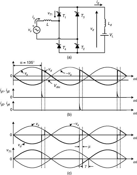
FIGURE 11.11 Rectifier in the inverting mode: (a) circuit; (b) waveforms neglecting source inductance L; and (c) waveforms considering L.
Figure 11.11b shows the waveform of the load voltage with the rectifier in the inverting mode, neglecting the source inductance L.
Section 11.2.6 described how supply inductance increases the conduction interval of the thyristors by the angle μ. As shown in Fig. 11.11c, the thyristor voltage vT1 has a negative value during the extinction angle γ defined by
![]() (11.23)
(11.23)
To ensure that the outgoing thyristor will recover its blocking capability after the commutation, the extinction angle should satisfy the following restriction
![]() (11.24)
(11.24)
where ω is the supply frequency and tq is the thyristor turn-off time. Considering Eqs. (11.23) and (11.24) the maximum firing angle is, in practice,
![]() (11.25)
(11.25)
If the condition of Eq. (11.25) is not satisfied, the commutation process will fail, originating destructive currents.
11.2.8 Applications
Important application areas of controlled rectifiers include uninterruptible power supplies (UPS), for feeding critical loads. Figure 11.12 shows a simplified diagram of a single-phase UPS configuration, typically rated for < 10 kVA. A fully controlled or half-controlled rectifier is used to generate the dc voltage for the inverter. In addition, the input rectifier acts as a battery charger. The output of the inverter is filtered before it is fed to the load. The most important operation modes of the UPS are:
(i) Normal mode. In this case the line voltage is present. The critical load is fed through the rectifier-inverter scheme. The rectifier keeps the battery charged.
(ii) Outage mode. During a loss of the ac main supply, the battery provides the energy for the inverter.
(iii) Bypass operation. When the load demands an over-current to the inverter, the static bypass switch is turned on and the critical load is fed directly from the mains.
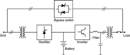
FIGURE 11.12 Application of a rectifier in single-phase UPS.
The control of low power dc motors is another interesting application of controlled single-phase rectifiers. In the circuit of Fig. 11.13, the controlled rectifier regulates the armature voltage and consequently controls the motor current id in order to produce a required torque.
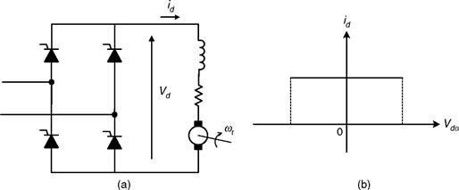
FIGURE 11.13 Two-quadrant de drive: (a) circuit and (b) quadrants of operation.
This configuration allows only positive current flow in the load. However the load voltage can be both positive and negative. For this reason, this converter works in the two-quadrant mode of operation in the plane id vs Vdα
A better performance can be obtained with two rectifiers in back-to-back connection at the dc terminals, as shown in Fig. 11.14a. This arrangement, known as a dual converter configuration, allows four-quadrant operation of the drive. Rectifier I provides positive load current id, while rectifier II provides negative load current. The motor can work in forward powering, forward braking (regenerating), reverse powering, and reverse braking (regenerating). These operating modes are shown in Fig. 11.14b, where the torque T vs the rotor speed ωr is illustrated.
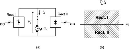
FIGURE 11.14 Single-phase dual-converter drive: (a) connection and (b) four-quadrant operation.
11.3 Unity Power Factor Single-phase Rectifiers
11.3.1 The Problem of Power Factor in Single-phase Line-commutated Rectifiers
The main disadvantages of the classical line-commutated rectifiers are that (i) they produce a lagging displacement factor with respect to the voltage of the utility; (ii) they generate an important amount of input current harmonics.
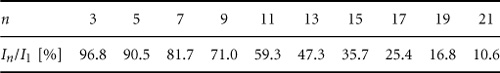
These aspects have a negative influence on both power factor and power quality. In the last several years, the massive use of single-phase power converters has increased the problems of power quality in electrical systems. In effect, modern commercial buildings have 50% and even up to 90% of the demand, originated by non-linear loads, which are composed mainly by rectifiers [1]. Today it is not unusual to find rectifiers with total harmonic distortion of the current THDi > 40%, originating severe overloads in conductors and transformers.
Figure 11.15a shows a single-phase rectifier with a capacitive filter, used in much of today’s low-power equipment. The input current produced by this rectifier is illustrated in Fig. 11.15b, it appears highly distorted due to the presence of the filter capacitor. This current has a harmonic content shown in Fig. 11.16 and Table 11.1, with a THDi, = 197%.
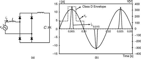
FIGURE 11.15 Single-phase rectifier: (a) circuit and (b) waveforms of the input voltage and current.
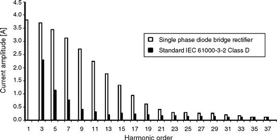
FIGURE 11.16 Input current harmonics produced by a single-phase diode bridge rectifier.
TABLE 11.1 Harmonic content of the current of Fig. 11.15
The rectifier in Fig. 11.15 has a very low power factor of PF = 0.45, due mainly to its large harmonic content.
11.3.2 Standards for Harmonies in Single-phase Rectifiers
The relevance of the problems originated by harmonics in single-phase line-commutated rectifiers has motivated some agencies to introduce restrictions to these converters. The IEC 61000-3-2 Class D International Standard establishes limits to all low-power single-phase equipment having an input current with a “special wave shape” and an active input power P ≤ 600 W. Class D equipment has an input current with a special wave shape contained within the envelope given in Fig. 11.15b. This class of equipment must satisfy certain harmonic limits, shown in Fig. 11.16. It is clear that a single-phase line-commutated rectifier with the parameters shown in Fig. 11.15a is not able to comply with the standard IEC 61000-3-2 Class D. The standard can be satisfied only by adding huge passive filters, which increases the size, weight, and cost of the rectifier. This standard has been the motivation for the development of active methods to improve the quality of the input current and, consequently, the power factor.
11.3.3 The Single-phase Boost Rectifier
One of the most important high power factor rectifiers, from a theoretical and conceptual point of view, is the so-called single-phase boost rectifier, shown in Fig. 11.17a, which is obtained from a classical non-controlled bridge rectifier, with the addition of transistor T, diode D, and inductor L.
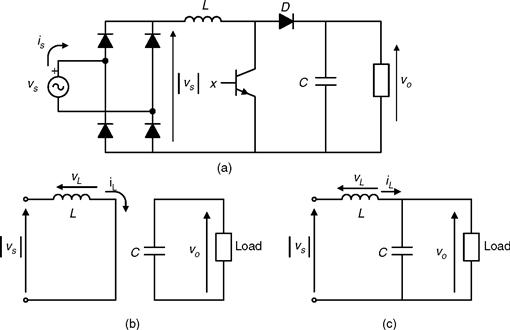
FIGURE 11.17 Single-phase boost rectifier: (a) power circuit and equivalent circuit for transistor T in; (b) on-state; and (c) off-state.
11.3.3.1 Working Principle, Basic Concepts
In boost rectifiers, the input current is(t) is controlled by changing the conduction state of transistor T. When transistor T is in the on-state, the single-phase power supply is short-circuited through the inductance L, as shown in Fig. 11.17b; the diode D avoids the discharge of the filter capacitor C through the transistor. The current of the inductance iL is given by the following equation
![]() (11.26)
(11.26)
Due to the fact that |vs| > 0, the on-state of transistor T always produces an increase in the inductance current iL and consequently an increase in the absolute value of the source current is.
When transistor T is turned off, the inductor current iL cannot be interrupted abruptly and flows through diode D, charging capacitor C. This is observed in the equivalent circuit of Fig. 11.17c. In this condition, the behavior of the inductor current is described by
![]() (11.27)
(11.27)
If vo > |vs|, which is an important condition for the correct behavior of the rectifier, then |vs| - vo < 0, and this means that in the off-state the inductor current decreases its instantaneous value.
11.3.3.2 Continuous Conduction Mode (CCM)
With an appropriate firing pulse sequence is applied to transistor T, the waveform of the input current is can be controlled to follow a sinusoidal reference, as can be observed in the positive half-wave of is in Fig. 11.18. This figure shows the reference inductor current iLref, the inductor current iL and the gate drive signal x for transistor T. Transistor T is on when x = 1 and it is off when x = 0.
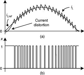
FIGURE 11.18 Behavior of the inductor current iL: (a) waveforms and (b) transistor T gate drive signal x.
Figure 11.18 clearly shows that the on- (off-) state of transistor T produces an increase (decrease) in the inductor current iL.
Note that for low values of vs the inductor does not have enough energy to increase the current value, for this reason it presents a distortion in their current waveform as shown in Fig. 11.18a.
Figure 11.19 presents a block diagram of the control system for the boost rectifier, which includes a proportional-integral (PI) controller, to regulate the output voltage vo. The reference value iLref for the inner current control loop is obtained from the multiplication between the output of the voltage controller and the absolute value |vs (t)|. A hysteresis controller provides a fast control for the inductor current iL, resulting in a practically sinusoidal input current is.
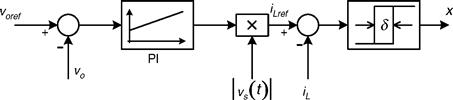
FIGURE 11.19 Control system of the boost rectifier.
Typically, the output voltage vo should be at least 10% higher than the peak value of the source voltage vs(t), in order to assure good dynamic control of the current. The control works with the following strategy: a step increase in the reference voltage voref will produce an increase in the voltage error voref -vo and an increase of the output of the PI controller, which originates an increase in the amplitude of the reference current iLref The current controller will follow this new reference and will increase the amplitude of the sinusoidal input current is, which will increase the active power delivered by the single-phase power supply, producing finally an increase in the output voltage vo.
Figure 11.20a shows the waveform of the input current isand the source voltage vs. The ripple of the input current can be reduced by shortening the hysteresis width δ The tradeoff for this improvement is an increase in the switching frequency, which is proportional to the commutation losses of the transistors. For a given hysteresis width δ, a reduction of inductance I also produces an increase in the switching frequency. As can be seen, the input current presents a third-harmonic component. This harmonic is generated by the second-harmonic component present in vo, which is fed back through the voltage (PI) controller and multiplied by the sinusoidal waveform, generating a third-harmonic component on iLref. This harmonic contamination can be avoided by filtering the vo measurement with a lowpass filter or a bandstop filter around 2ωs. The input current obtained using the measurement filter is shown in Fig. 11.20b. Figure 11.20d confirms the reduction of the third-harmonic component.
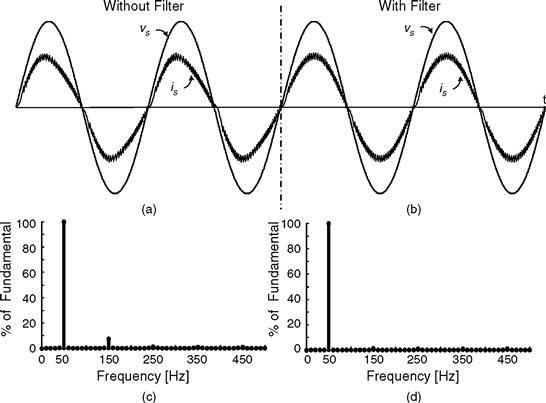
FIGURE 11.20 Input current and voltage of the single-phase boost rectifier: (a) without a filter on vo measurement; (b) with a filter on vo measurement; frequency spectrum; (c) without filter; and (d) with filter.
However, in both cases, a drastic reduction in the harmonic content of the input current is can be observed in the frequency spectrum of Figs. 11.20c and 11.20d. This current fulfills the restrictions established by standard IEC 61000-3-2. The total harmonic distortion of the current in Fig. 11.20a is THD = 7.46%, while the THD of the current of Fig. 11.20b is 4.83%, in both cases a very high power factor, over 0.99, is reached.
Figure 11.21 shows the dc voltage control loop dynamic behavior for step changes in the load. An increase in the load, at t = 0.3 [s], produces an initial reduction of the output voltage vo, which is compensated by an increase in the input current is. At t = 0.6 [s] a step decrease in the load is applied. The dc voltage controller again adjusts the supply current in order to balance the active power.
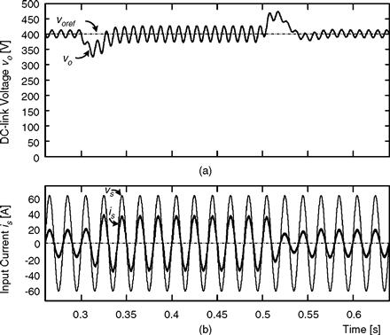
FIGURE 11.21 Response to a change in the load: (a) output-voltage vo and (b) input current is.
11.3.3.3 Discontinuous Conduction Mode (DCM)
This PFC method is based on an active current waveform-shaping principle. There are two different approaches considering fixed and variable switching frequency, both operating principles are illustrated in Fig. 11.22.
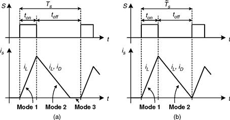
FIGURE 11.22 Boost DCM operating principle: (a) with fixed switching frequency and (b) with variable switching frequency.
a) DCM with Fixed Switching Frequency
The current shaping strategy is achieved by combining three different conduction modes, performed over a fixed switching period Ts. At the beginning of each period the power semiconductor is turned on. During the on-state, shown in Fig. 11.23a, the power supply is short-circuited through the rectifier diodes, the inductor L, and the boost switch T. Hence, the inductor current iL increases at a rate proportional to the instantaneous value of the supply voltage. As a result, during the on-state, the average supply current is is proportional to the supply voltage vs which yields to power factor correction.
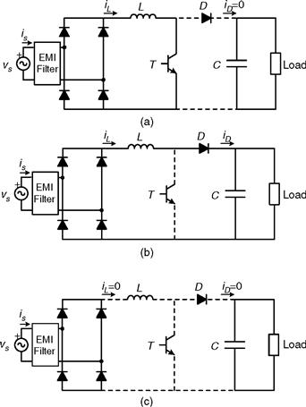
FIGURE 11.23 Boost DCM equivalent circuits: (a) mode 1: transistor on, inductor current increasing; (b) mode 2: transistor off, inductor current decreasing; and (c) mode 3: transistor off, inductor current reaches zero.
When the switch is turned off, the current flows to the load trough diode D, as shown in Fig. 11.23b. The instantaneous current value decreases (since the load voltage vo is higher than the supply peak voltage) at a rate proportional to the difference between the supply and load voltage. Finally, the last mode, illustrated in Fig. 11.23c, corresponds to the time in which the current reaches zero value, completing the switching period Ts. Therefore, the supply current is not proportional to the voltage source during the whole control period, introducing distortion and undesirable EMI in comparison to CCM.
The duty cycle D = ton/Ts is determined by the control loop, in order to obtain the desired output power and to ensure operation in DCM, i.e. to reach zero current before the new switching cycle starts. The control strategy can be implemented with analog circuitry as shown in Fig. 11.24, or digitally with modern computing devices. Generally, the duty cycle is controlled with a slow control loop, maintaining the output voltage and duty cycle constant over a half-source cycle.
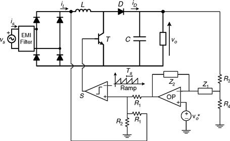
FIGURE 11.24 Boost DCM control circuit with fixed switching frequency.
A qualitative example of the supply voltage and current obtained using DCM is illustrated in Fig. 11.25.
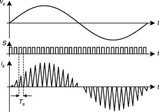
FIGURE 11.25 Boost DCM waveforms: supply voltage, transistor control signal, and supply current.
b) DCM with Variable Switching Frequency
The operating principle is similar to the one used in the previous case, the main difference is that mode 3 is avoided by switching the transistor again to the on-state, immediately after the inductor current reaches zero value. This reduces the current distortion, with the tradeoff of introducing variable switching frequency (Ts is variable) and consequently lower-order harmonic content.
Both CCM and DCM achieve an improvement in the power factor. The DCM is more efficient since reverse-recovery losses of the boost diode are eliminated, however this mode introduces high-current ripple and considerable distortion and usually an important fifth-order harmonic is obtained. Therefore boost-DCM applications are limited to 300 W power levels, to meet standards and regulations. The DCM with variable switching frequency reduces this harmonic content, at expends of a wide distributed current spectrum and all related design problems.
11.3.3.4 Resonant Structures for the Boost Rectifiers
An important issue in power electronics is the power losses in power semiconductors. These losses can be classified in two groups: conduction losses and switching losses, as shown in Fig. 11.26.
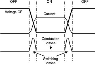
FIGURE 11.26 Conduction and switching losses on a power switch.
The conduction losses are produced by the current through the semiconductor juncture, so these losses are unavoidable. However, the switching losses, which are produced while the power semiconductors work in linear state during the transition from on- to off- state or from off- to on-state, can be reduced or even eliminated, if the switch (transition) occurs when: (a) the current across the power semiconductor is zero; (b) the voltage between the power terminals of the power semiconductor is zero.
This operation mode is used in the so-called resonant or soft-switched converters, which are discussed in detail in a different chapter of this handbook.
Resonant operation can also be used with the boost converter topology. In order to produce this condition, topology of Fig. 11.17 needs to be modified, by including reactive components and additional semiconductors.
In Fig. 11.27 a resonant structure for zero current switching (ZCS) [2] is shown. As can be seen, additional resonant inductors (Lr1, Lr2), capacitors (Cr), diodes (Dr1, Dr2), and power switch (Sr) have been included.
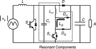
FIGURE 11.27 Boost rectifier with ZCS.
In a similar way, in Fig. 11.28 a resonant structure for zero voltage switching (ZVS) [3] is shown. Once again, additional inductance (Lr), capacitor (Cr), and power switch (Sr) are added, note however, that diode D has been replaced by two “resonant diodes,” Dr1 and Dr2.
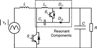
FIGURE 11.28 Boost rectifier with ZVS.
In both cases, the ZVS or ZCS condition is reached through a proper control of Sr. Other resonant topologies are described in the literature [4–6] with similar behavior.
11.3.3.5 Bridgless Boost Rectifier
The bridgless boost rectifier [7] is shown in Fig. 11.29a. This rectifier replaces the input diode rectifier by a combination of two boost rectifiers which work alternately: (a) when vs is positive, T1 and Di operate as boost rectifier 1 (Fig. 11.29b); (b) when vs is negative, T2 and D2 operate as boost rectifier 2 (Fig. 11.29c);
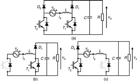
FIGURE 11.29 (a) Power circuit of bridgless boost rectifier; equivalent circuit when; (b) vs > 0; and (c) vs < 0.
This topology reduces the conduction losses of the rectifier [8, 9], but requires a slightly more complex control scheme, also EMI and EMC aspects must be considered.
11.3.4 Voltage Doubler PWM Rectifier
Figure 11.30a shows the power circuit of the voltage doubler pulse width modulated (PWM) rectifier, which uses two transistors T1 and T2 and two filter capacitors C1 and C2. The transistors are switched complementary to control the waveform of the input current is and the output dc voltage vo. Capacitor voltages VC1 and VC2 must be higher than the peak value of the input voltage vs to ensure the control of the input current.
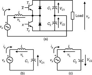
FIGURE 11.30 Voltage doubler rectifier: (a) power circuit; (b) equivalent circuit with T1 on; and (c) equivalent circuit with T2 on.
The equivalent circuit of this rectifier with transistor T1 in the on-state is shown in Fig. 11.30b. For this case, the inductor voltage dynamic equation is
![]() (11.28)
(11.28)
Equation (11.28) means that under this conduction state, current is(t) decreases its value.
On the other hand, the equivalent circuit of Fig. 11.30c is valid when transistor T2 is in the conduction state, resulting in the following expression for the inductor voltage
![]() (11.29)
(11.29)
hence, for this condition, the input current is(t) increases.
Therefore the waveform of the input current can be controlled by switching appropriately transistors T1 and T2 in a similar way as shown in Fig. 11.18a for the single-phase boost converter. Figure 11.31 shows a block diagram of the control system for the voltage doubler rectifier, which is very similar to the control scheme of the boost rectifier. This topology can present an unbalance in the capacitor voltages VC1 and VC2, which will affect the quality of the control. This problem is solved by adding to the actual current value is an offset signal proportional to the capacitor’s voltage difference.
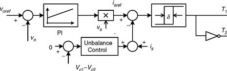
FIGURE 11.31 Control system of the voltage doubler rectifier.
Figure 11.32 shows the waveform of the input current. The ripple amplitude of this current can be reduced by decreasing the hysteresis width of the controller.
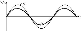
FIGURE 11.32 Waveform of the input current in the voltage doubler rectifier.
11.3.5 The PWM Rectifier in Bridge Connection
Figure 11.33a shows the power circuit of the fully controlled single-phase PWM rectifier in bridge connection, which uses four transistors with antiparallel diodes to produce a controlled dc voltage vo. Using a bipolar PWM switching strategy, this converter may have two conduction states: (i) Transistors T1 and T4 in the on-state and T2 and T3 in the off-state; (ii) Transistors T2 and T3 in the on-state and T1 and T4 in the off-state.
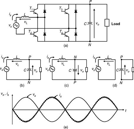
FIGURE 11.33 Single-phase PWM rectifier in bridge connection: (a) power circuit; (b) equivalent circuit with T1 and T4 on; (c) equivalent circuit with T2 and T3 on; (d) equivalent circuit with T1 and T3 or T2 and T4 on; and (e) waveform of the input current during regeneration.
In this topology, the output voltage vo must be higher than the peak value of the ac source voltage vs, to ensure a proper control of the input current.
Figure 11.33b shows the equivalent circuit with transistors T1 and T4 on. In this case, the inductor voltage is given by
![]() (11.30)
(11.30)
Therefore, in this condition a reduction of the inductor current is is produced.
Figure 11.33c shows the equivalent circuit with transistors T2 and T3 on. Here, the inductor voltage has the following expression
![]() (11.31)
(11.31)
which means an increase in the instantaneous value of the input current is.
Finally, Fig. 11.33d shows the equivalent circuit with transistors T1 and T3 or T2 and T4 are in the on-state. In this case, the input voltage source is short-circuited through inductor L, which yields
![]() (11.32)
(11.32)
Equation (11.32) implies that the current value will depend on the sign of vs.
The waveform of the input current is can be controlled by appropriately switching transistors T1–T4 or T2–T3, originating a similar shape to the one shown in Fig. 11.18a for the single-phase boost rectifier.
The control strategy for the rectifier is similar to the one illustrated in Fig. 11.31, for the voltage doubler topology. The quality of the input current obtained with this rectifier is the same as presented in Fig. 11.32 for the voltage doubler configuration.
The input current waveform can be slightly improved if the state of Fig. 11.33d is used. This can be done by replacing the hysteresis current control with a more complex linear control plus a three-level PWM modulator. This method reduces the semiconductor switching frequency and provides a more defined current spectrum.
Finally, it must be said that one of the most attractive characteristics of the fully controlled PWM converter in bridge connection and the voltage doubler is their regeneration capability. In effect, these rectifiers can deliver power from the load to the single-phase supply, operating with sinusoidal current and a high power factor of PF > 0.99. Figure 11.33e shows that during regeneration, the input current is is 180° out of phase with respect to the supply voltage vs, which means operation with power factor PF ≈ − 1 (PF is approximately 1 because of the small harmonic content in the input current).
11.3.6 Applications of Unity Power Factor Rectifiers
11.3.6.1 Boost Rectifier Applications
The single-phase boost rectifier has become the most popular topology for power factor correction (PFC) in general purpose power supplies. To reduce the costs, the complete control system shown in Fig. 11.19 and the gate drive circuit of the power transistor have been included in a single integrated circuit (IC), like the UC3854 [10] or MC33262, shown in Fig. 11.34.
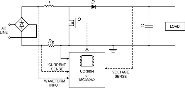
FIGURE 11.34 Simplified circuit of a power factor corrector with control integrated circuit.
Today there is increased interest in developing high-frequency electronic ballasts to replace the classical electromagnetic ballast present in fluorescent lamps. These electronic ballasts require an ac–dc converter. To satisfy the harmonic current injection from electronic equipment and to maintain a high power quality, a high power factor rectifier can be used, as shown in Fig. 11.35 [11].
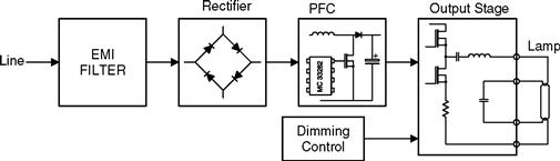
FIGURE 11.35 Functional block diagram of electronic ballast with power factor correction.
11.3.6.2 Voltage Doubler PWM Rectifier
The development of low-cost compact motor drive systems is a very relevant topic, particularly in the low-power range. Figure 11.36 shows a low-cost converter for low-power induction motor drives. In this configuration, a three-phase induction motor is fed through the converter from a single-phase power supply. Transistors T1, T2 and capacitors C1, C2constitute the voltage doubler single-phase rectifier, which controls the dc link voltage and generates sinusoidal input current, working with close-to-unity power factor [12]. On the other hand, transistors T3, T4, T5, and T6 and capacitors C1 and C2 constitute the power circuit of an asymmetric inverter that supplies the motor. An important characteristic of the power circuit shown in Fig. 11.36 is the capability of regenerating power to the single-phase mains.

FIGURE 11.36 Low-cost induction motor drive.
11.3.6.3 PWM Rectifier in Bridge Connection
Distortion of the input current in the line-commutated rectifiers with capacitive filtering is particularly critical in the UPS fed from motor-generator sets. In effect, due to the higher value of the generator impedance, the current distortion can originate an unacceptable distortion on the ac voltage, which affects the behavior of the whole system. For this reason, it is very attractive to use rectifiers with low distortion in the input current.
Figure 11.37 shows the power circuit of a single-phase UPS, which has a PWM rectifier in bridge connection at the input side. This rectifier generates a sinusoidal input current and controls the charge of the battery [13].
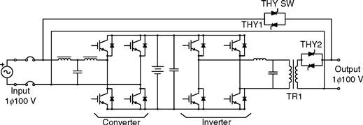
FIGURE 11.37 Single-phase UPS with PWM rectifier.
Perhaps the most typical and widely accepted area of application of high power factor single-phase rectifiers is in locomotive drives [14]. An essential prerequisite for proper operation of voltage source three-phase inverter drives in modern locomotives is the use of four-quadrant line-side converters, which ensure motoring and braking of the drive, with reduced harmonics in the input current. Figure 11.38 shows a simplified power circuit of a typical drive for a locomotive connected to a single-phase power supply [14], which includes a high power factor rectifier at the input.
FIGURE 11.38 Typical power circuit of an ac drive for locomotive.
Finally, Fig. 11.39 shows the main circuit diagram of the 300 series Shinkansen train [15]. In this application, ac power from the overhead catenary is transmitted through a transformer to single-phase PWM rectifiers, which provide the dc voltage for the inverters. The rectifiers are capable of controlling the input ac current in an approximate sine waveform and in phase with the voltage, achieving power factor close to unity on powering and on regenerative braking. Regenerative braking produces energy savings and an important operational flexibility.
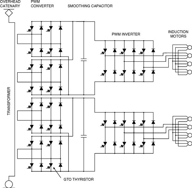
FIGURE 11.39 Main circuit diagram of 300 series Shinkansen locomotives.
Acknowledgment
The authors gratefully acknowledge the valuable contribution of Dr. Rubén Peña, and support provided by the Millennium Science Initiative (ICM) from Mideplan, Chile.
REFERENCES
1. Dwyer R, Mueller D. Selection of transformers for comercial buildings. In: Proc. of IEEE/IAS 1992 Annual Meeting, U.S.A. Oct 1992. [pp. 1335–1342].
2. Martins DC, de Seixas FJM, Brilhante JA, Barbi I. A family of dc-to-dc PWM converters using a new ZVS commutation cell. In: Proc. IEEE PESC’ 93. 1993. [pp. 524–530].
3. Bassett J. New, zero voltage switching, high frequency boost converter topology for power factor correction. In: Proc. INTELEC’ 95. 1995. [pp. 813–820].
4. Streit R, Tollik D. High efficiency telecom rectifier using a novel soft-switched boost-based input current shaper. In: Proc. INTELEC’ 91. 1991. [pp. 720–726].
5. Y. Jang and M. M. Jovanovic′, “A new, soft-switched, high-power-factor boost converter with IGBTs,” presented at the INTELEC’ 99, 1999, Paper 8-3.
6. Jovanovic′ MM. A technique for reducing rectifier reverse-recovery-related losses in high-voltage, high-power boost converters. In: Proc. IEEE APEC’ 97. 1997. [pp. 1000–1007].
7. Mitchell DM. AC-DC converter having an improved power factor. U.S. Patent 4. Oct 25, 1983; 412 [].
8. de Souza AF, Barbi I. A new ZVS-PWM unity power factor rectifier with reduced conduction losses. IEEE Trans. Power Electron. Nov 1995; vol. 10 [pp. 746–752].
9. de Souza AF, Barbi I. A new ZVS semiresonant power factor rectifier with reduced conduction losses. IEEE Trans. Ind. Electron. Feb 1999; vol. 46 [pp. 82–90].
10. P. Todd, “UC3854 controlled power factor correction circuit design,” Application Note U-134, Unitrode Corp.
11. Adams J, Ribarich T, Ribarich J. A new control IC for dimmable high-frequency electronic ballast. IEEE Applied Power Electronics Conference APEC’ 99, USA. 1999 [pp. 713–719].
12. Jacobina C, Beltrao M, Cabral E, Nogueira A. Induction motor drive system for low-power applications. IEEE Transactions on Industry Applications. Jan/Feb 1999; vol. 35(No. 1):52–60.
13. Hirachi K, Yamamoto H, Matsui T, Watanabe S, Nakaoka M. Cost-effective practical developments of high-performance 1kVA UPS with new system configurations and their specific control implementations. European Conference on Power Electronics EPE 95, Spain. 1995; 2035–2040.
14. HÜckelheim K, Mangold Ch. Novel 4-quadrant converter control method. European Conference on Power Electronics. 1989; 573–576.
15. Ohmae T, Nakamura K. Hitachi’s role in the area of power electronics for transportation. Proc. of the IECON’ 93. Hawai. Nov 1993; 714–718.