
• Mode A (Quadrant I): electrical energy is transferred from Vh side to VL side;
• Mode B (Quadrant II): electrical energy is transferred from VL side to VH side.
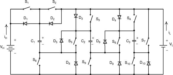
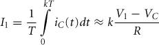
FIGURE 14.75 Two-quadrant switched-capacitor DC/DC Luo-converter.
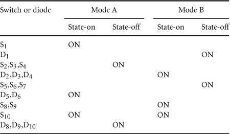
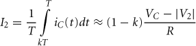
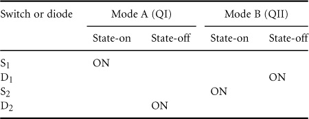
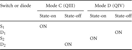
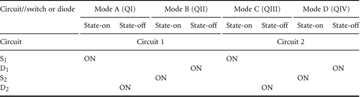
Each mode has two states: “on” and “off.” Usually, each state is operating in different conduction duty k. The switching period is T where T = 1/f, where f is the switching frequency. The switches are the power MOSFET devices. The parasitic resistance of all switches is rS. The equivalent resistance of all capacitors is rC and the equivalent voltage drop of all diodes is VD Usually we select the three capacitors having same capacitance C = C1 = C2 = C3. Some reference data are useful: rs = 0.03 ω, rC = 0.02 O, and VD = 0.5 V, f = 5 kHz, and C = 5000 μ F. The switch's status is shown in Table 14.5.
TABLE 14.5 Switch's status (the blank status means OFF)
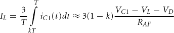
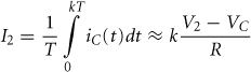
For Mode A, state-on is shown in Fig. 14.76a: switches S1 and S10 are closed and diodes D5 and D5 are conducted. Other switches and diodes are open. In this case capacitors C1, C2, and C3 are charged via the circuit VH -S1-C1-D5-C2-D6-C3-S10, and the voltage across capacitors C1, C2, and C3 is increasing. The equivalent circuit resistance is Ran = (2rs + 3rC) = 0.12 ω, and the voltage deduction is 2VD = 1V. State-off is shown in Fig. 14.76b: switches S2, S3, and S4 are closed and diodes D8, D9, and D10 are conducted. Other switches and diodes are open. In this case capacitor C1 (C2 and C3) is discharged via the circuit S2(S3 and S4)-VL -D8 (D9 and D10)-C1(C2 and C3), and the voltage across capacitor C1(C2 and C3) is decreasing. Mode A implements the current-amplification technique. The voltage and current waveforms are shown in Fig. 14.76c. All three capacitors are charged in series during state-on. The input current flows through three capacitors and the charges accumulated on the three capacitors should be the same. These three capacitors are discharged in parallel during state-off. Therefore, the output current is amplified by three times.
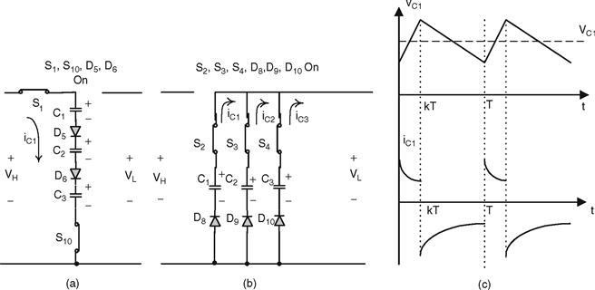
FIGURE 14.76 Mode A operation: (a) state-on; (b) state-off; and (c) voltage and current waveforms.
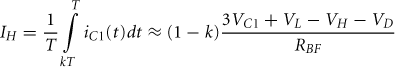
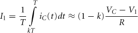
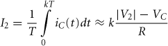
The variation of the voltage across capacitor C1 is:
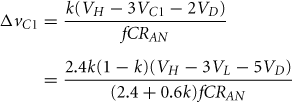
After calculation,
The average output current is
The average input current is
Therefore, we have 3IH = IL.
Output power is
The transfer efficiency is
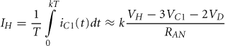
For Mode B, state-on is shown in Fig. 14.77a: switches S8, S9, and S10 are closed and diodes D2, D3, and D4 are conducted. Other switches and diodes are off. In this case all three capacitors are charged via each circuit VL-D2 (and D3, D4)-C1 (and C2, C3)-S8 (and S9, S10), and the voltage across three capacitors are increasing. The equivalent circuit resistance is Rbn = rs + rC and the voltage deduction is VD; in each circuit. State-off is shown in Fig. 14.77b: switches S5, S6, and S7 are closed and diode D1 is on. Other switches and diodes are open. In this case all capacitors is discharged via the circuit VL-S7-C3-S6-C2-S5-C1-D1-VH, and the voltage across all capacitors is decreasing. Mode B implements the voltage-lift technique. The voltage and current waveforms are shown in Fig. 14.77c. All three capacitors are charged in parallel during state-on. The input voltage is applied to the three capacitors symmetrically, so that the voltages across these three capacitors should be same. They are discharged in series during state-off. Therefore, the output voltage is lifted by three times.
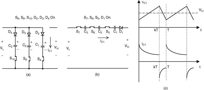
FIGURE 14.77 Mode B operation: (a) state-on; (b) state-off; and (c) voltage and current waveforms.
The variation of the voltage across capacitor C is:
After calculation
The average input current is
The average output current is
From this formula, we have 4IH = IL.
Input power is
Output power is
14.8.2 Four-quadrant Switched-capacitor DC/DC Luo-converter
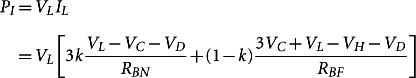
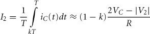
Four-quadrant switched-capacitor DC/DC Luo-converter is shown in Fig. 14.78. Since it performs the voltage-lift technique, it has a simple structure with four-quadrant operation. This converter consists of eight switches and two capacitors. The source voltage V1 and load voltage V2 (e.g. a battery or DC motor back EMF) are usually constant voltages. In this paper they are supposed to be ± 21V and ± 14V. Capacitors C1 and C2 are same and C1 = C1 = 2000 μF. The circuit equivalent resistance R = 50 mΩ. Therefore, there are four modes of operation for this converter:
1. Mode A: energy is converted from source to positive voltage load; the first-quadrant operation, QI;
2. Mode B: energy is converted from positive voltage load to source; the second-quadrant operation, QII;
3. Mode C: energy is converted from source to negative voltage load; the third-quadrant operation, QIII;
4. Mode D: energy is converted from negative voltage load to source; the fourth-quadrant operation, QIV.
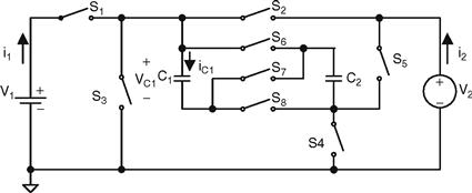
FIGURE 14.78 Four-quadrant sc DC/DC Luo-converter.
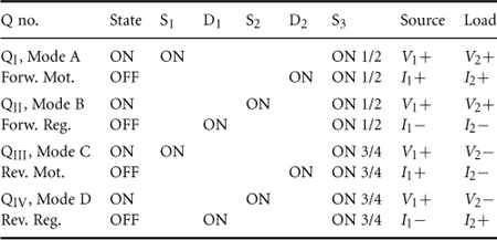
The first-quadrant (Mode A) is so called the forward motoring (Forw. Mot.) operation. V1 and V2 are positive, and I1 and I2 are positive as well. The second-quadrant (Mode B) is so called the forward regenerative (Forw. Reg.) braking operation. V1 and V2 are positive, and I1 and I2 are negative. The third-quadrant (Mode C) is so-called the reverse motoring (Rev. Mot.) operation. V1 and I1 are positive, and V2 and I2 are negative. The fourth-quadrant (Mode D) is so-called the reverse regenerative (Rev. Reg.) braking operation. V1 and I2 are positive, and I1 and V2 are negative.
Each mode has two conditions: V1 > V2 and V1 < V2 (or |V2| for QIII and QIV). Each condition has two states: “on” and “off.” Usually, each state is operating in various conduction duty k for different currents. As usual, the efficiency of all SC DC/DC converters is independent from the conduction duty cycle k. The switching period is T where T = 1/f. The switch status is shown in Table 14.6.
TABLE 14.6 Switch's status (mentioned switches are not open)
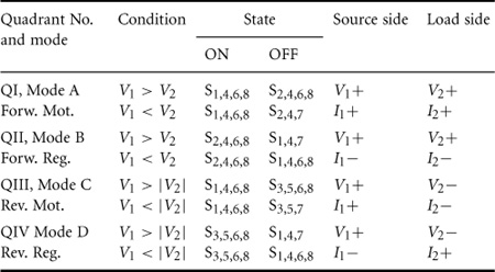
As usual, the transfer efficiency only relies on the ratio of the source and load voltages, and it is independent on R, C, f, and k. We select k = 0.5 for our description. Other values for the reference are f = 5kHz, V1 = 21 V, V2 = 14V, and total C = 4000 µF, R = 50 mΩ.
For Mode Al, condition V1 > V2 is shown in Fig. 14.78a. Since V1 > V2, two capacitors C1 and C2 are connected in parallel. During switch-on state, switches S1, S4, S6, and S8 are closed and other switches are open. In this case, capacitors C1//C2 are charged via the circuit V1–S1–C1//C2-S4, and the voltage across capacitors C1 and C2 is increasing. During switch-off state, switch S2, S4, S6, and S8 are closed and other switches are open. In this case capacitors C1//C2 are discharged via the circuit S2-V2-S4-C1//C2, and the voltage across capacitors C1 and C2 is decreasing. Capacitors C1 and C2 transfer the energy from the source to the load.
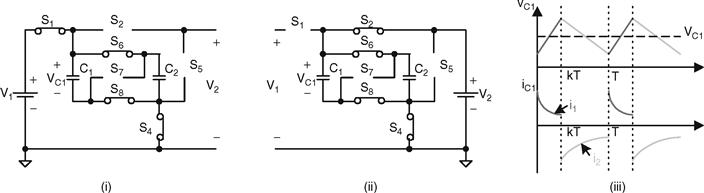
FIGURE 14.78a Mode Al (QI): forward motoring with V1 > V2: (i) switch on: S1, S4, S6, and S8 on; (ii) switch off: S2, S4, S6, and S8, on; and (iii) waveforms.
The average capacitor voltage
and

The transfer efficiency is
For Mode A2, condition V1 < V2 is shown in Fig. 14.78b. Since V1 < V2, two capacitors C1 and C2 are connected in parallel during switch on and in series during switch off. This is so-called the voltage-lift technique. During switch-on state, switches S1, S4, S6, and S8 are closed and other switches are open. In this case, capacitors C1//C2 are charged via the circuit V1-S1-C1//C2-S4, and the voltage across capacitors C1 and C2 is increasing. During switch-off state, switches S2, S4, and S7 are closed and other switches are open. In this case, capacitors C1 and C2 are discharged via the circuit S2-V2-S4-C1-S7-C2, and the voltage across capacitor C1 and C2 is decreasing. Capacitors C1 and C2 transfer the energy from the source to the load.

FIGURE 14.78b Mode A2 (QI): forward motoring with V1 < V2: (i) switch on: S1, S4, S6, and S8, on; (ii) switch off: S2, S4, and S7, on; and (iii) waveforms.
The average capacitor voltage is
The average current is
and
For Mode B1, condition V1 > V2 is shown in Fig. 14.78c. Since V1 > V2, two capacitors C1 and C2 are connected in parallel during switch on and in series during switch off. The voltage-lift technique is applied. During switch-on state, switches S2, S4, S6, and S8 are closed. In this case, capacitors C1//C2 are charged via the circuit V2-S2-C1//C2-S4, and the voltage across capacitors C1 and C2 is increasing. During switch-off state, switches S1, S4, and S7 are closed. In this case, capacitors C1 and C2 are discharged via the circuit S1-V1-S4-C2-S7-C1, and the voltage across capacitor C1 and C2 is decreasing. Capacitors C1 and C2 transfer the energy from the load to the source. Therefore, we have I2 = 2I1.
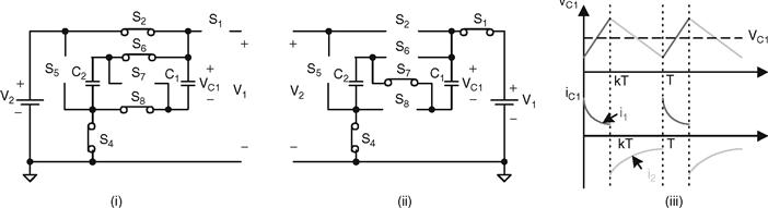
FIGURE 14.78c Mode BI (QII): forward regenerative braking with V1 > V2: (i) switch on: S2, S4, S6, and S8, on; (ii) switch off; S1, S4(S5), and S7 on; and (iii) waveforms.
The average capacitor voltage is
The average current is
and
The transfer efficiency is
For Mode B2, condition V1 < V2 is shown in Fig. 14.78d. Since V1 < V2, two capacitors C1 and C2 are connected in parallel. During switch-on state, switches S2, S4, S6, and S8 are closed. In this case, capacitors C1//C2 are charged via the circuit V2-S2-C1//C2-S4, and the voltage across capacitors C1 and C2is increasing. During switch-off state, switches S1, S4, S6, and S8 are closed. In this case capacitors C1//C2 is discharged via the circuit S1-V1-S4-C1//C2, and the voltage across capacitors C1 and C2 is decreasing. Capacitors C1 and C2 transfer the energy from the load to the source. Therefore, we have I2 = I1.
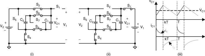
FIGURE 14.78d Mode B2 (QII): forward regenerative braking with V1 < V2: (i) switch on: S2, S4, S6, and S8, on; (ii) switch off: S1, S4(S5), S6, and S8 on; and (iii) waveforms.
The average capacitor voltage is
The average current is
and

The transfer efficiency is
For Mode C1, condition V1 > | V2| is shown in Fig. 14.78e. Since V1 > | V2|, two capacitors C1 and C2 are connected in parallel. During switch-on state, switches S1, S4, S6, and S8 are closed. In this case, capacitors C1//C2 are charged via the circuit V1-S1-C1//C2-S4, and the voltage across capacitors C1 and C2 is increasing. During switch-off state, switches S3, S5, S6, and S8 are closed. Capacitors C1 and C2 are discharged via the circuit S3-V2-S5-C1//C2, and the voltage across capacitors C1 and C2 is decreasing. Capacitors C1 and C2 transfer the energy from the source to the load. We have I1 = I2.

FIGURE 14.78e Mode C1 (QUI): reverse motoring with V1 > |V2|: (i) switch on: S1, S4, S6, and S8 on; (ii) switch off: S3, S5, S6, and S8 on; and (iii) waveforms.
The average capacitor voltage is
The average current (absolute value) is
and the average input current is

The transfer efficiency is
For ModeC2, condition V1 < |V2| is shown in Fig. 14.78f. Since V1 < |V2|, two capacitors C1 and C2 are connected in parallel during switch on and in series during switch off, applying the voltage-lift technique. During switch-on state, switches S1, S4, S6, and S8, are closed. Capacitors C1 and C2 are charged via the circuit V1-S1-C1//C2-S4, and the voltage across capacitors C1 and C2 is increasing. During switch-off state, switches S3, S5, and S7 are closed. Capacitors C1 and C2 is discharged via the circuit S3-V2-S5-C1-S7-C2, and the voltage across capacitor C1 and C2 is decreasing. Capacitors C1 and C2 transfer the energy from the source to the load. We have I1 = 2I2.
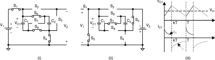
FIGURE 14.78f Mode C2 (QUI): reverse motoring with V1 < | V2|: (i) switch on: S1, S4, S6, and S8, on; (ii) switch off: S3, S5, and S7, on; and (iii) waveforms.
The average capacitor voltage is
and
The transfer efficiency is
For Mode D1, condition V1 > |V2| is shown in Fig. 14.78g. Since V1 > |V2|, two capacitors C1 and C2 are connected in parallel during switch on and in series during switch off, applying the voltage-lift technique. During switch-on state, switches S3, S5, S6, and S8 are closed. In this case, capacitors C1//C2 are charged via the circuit V2-S3-C1//C2-S5, and the voltage across capacitors C1 and C2 is increasing. During switch-off state, switches S1, S4, and S7 are closed. Capacitors C1 and C2 are discharged via the circuit S1-V1-S4-C2-S7-C1, and the voltage across capacitor C1 and C2 is decreasing. Capacitors C1 and C2 transfer the energy from the load to the source. We have I2 = 2I1.
FIGURE 14.78g Mode Dl (QIV): reverse regenerative braking with V1 > |V2|: (i) switch on: S3, S4, S6, and S8, on; (ii) switch off: S1, S4, and S7 on; and (iii) waveforms.
The average capacitor voltage is
The average currents are
and
For Mode D2, condition V1 < |V2| is shown in Fig. 14.78h. Since V1 < |V2|, two capacitors C1 and C2 are connected in parallel. During switch-on state, switches S3, S5, S6, and S8 are closed. In this case, capacitors C1//C2 are charged via the circuit V2-S3-C1//C2-S5, and the voltage across capacitors C1 and C2 is increasing. During switch-off state, switches S1, S4, S6, and S8 are closed. Capacitors C1 and C2 are discharged via the circuit S1-V1-S4-C1//C2, and the voltage across capacitors C1 and C2 is decreasing. Capacitors C1 and C2 transfer the energy from the load to the source. We have I2 = I1.
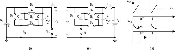
FIGURE 14.78h Mode D2 (QIV): reverse regenerative braking with V1 < |V2|: (i) switch on: S3, S5, S6, and S8, on; (ii) switch off: S1, S4, S6, and S8 on; and (iii) waveforms.
The average capacitor voltage is
The average currents are

and
The transfer efficiency is
14.9 Multiple-lift Push–Pull Switched-capacitor Luo-converters
Micro-power-consumption technique requires high power density DC/DC converters and power supply source. Voltage-lift (VL) technique is a popular method to apply in electronic circuit design. Since switched-capacitor can be integrated into power integrated circuit (IC) chip, its size is small. Combining switched-capacitor and VL techniques the DC/DC converters with small size, high power density, high voltage transfer gain, high power efficiency, and low EMI can be constructed. This section introduces a new series DC/DC converters –multiple-lift push-pull switched-capacitor DC/DC Luo-converters. There are two subseries:
• P/O multiple-lift (ML) push-pull (PP) switched-capacitor (SC) DC/DC Luo-converter;
• N/O multiple-lift push-pull switched-capacitor DC/DC Luo-converter.
14.9.1 P/O Multiple-lift Push–Pull Switched-capacitor DC/DC Luo-converter
P/O ML-PP SC DC/DC Luo-converters have several subseries:
We only introduce three circuits of main series and additional series in this section.
P/O ML-PP SC Luo-converter elementary circuit is shown in Fig. 14.79a. Its output voltage and current are
FIGURE 14.79 P/O ML-PP SC Luo-converter: (a) elemental; (b) re-lift; and (c) triple-lift circuits.
The voltage transfer gain is
P/O ML-PP SC Luo-converter re-lift circuit is shown in Fig. 14.79b. Its output voltage and current are
and
The voltage transfer gain is
P/O ML-PP SC Luo-converter triple-lift circuit is shown in Fig. 14.79c. Its output voltage and current are
and
The voltage transfer gain is
P/O ML-PP SC Luo-converter additional circuit is shown in Fig. 14.80a. Its output voltage and current are
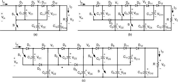
FIGURE 14.80 P/O ML-PP SC Luo-converter re-lift circuit: (a) additional; (b) re-lift; and (c) triple-lift circuits.
and
The voltage transfer gain is
P/O ML-PP SC Luo-converter additional re-lift circuit is shown in Fig. 14.80b. Its output voltage and current are
and
The voltage transfer gain is
P/O ML-PP SC Luo-converter additional triple-lift circuit is shown in Fig. 14.80c. Its output voltage and current are
and
The voltage transfer gain is
14.9.2 N/O Multiple-lift Push–Pull Switched-capacitor DC/DC Luo-converter
N/O ML-PP SC DC/DC Luo-converters have several subseries:
We only introduce three circuits of main series and additional series in this section.
N/O ML-PP SC Luo-converter elementary circuit is shown in Fig. 14.81a. Its output voltage and current are
FIGURE 14.81 N/O ML-PP SC Luo-converter: (a) elemental; (b) re-lift; and (c) triple-lift circuits.
and
The voltage transfer gain is
N/O ML-PP SC Luo-converter re-lift circuit is shown in Fig. 14.81b. Its output voltage and current are
and
The voltage transfer gain is
N/O ML-PP SC Luo-converter triple-lift circuit is shown in Fig. 14.81c. Its output voltage and current are
and
N/O ML-PP SC Luo-converter additional circuit is shown in Fig. 14.82a. Its output voltage and current are

FIGURE 14.82 N/O ML-PP SC Luo-converter re-lift circuit: (a) additional; (b) re-lift; and (c) triple-lift circuits.
and
The voltage transfer gain is
N/O ML-PP SC Luo-converter additional re-lift circuit is shown in Fig. 14.82b. Its output voltage and current are
and
The voltage transfer gain is
N/O ML-PP SC Luo-converter additional triple-lift circuit is shown in Fig. 14.82c. Its output voltage and current are
and
The voltage transfer gain is
14.10 Switched-inductor Multi-quadrant Operation Luo-converters
Switched-capacitor converters usually have many switches and capacitors, especially for the system with high ratio between source and load voltages. Switched-inductor converter usually has only one inductor even if it works in single-, two-, and/or four-quadrant operation. Simplicity is the main advantage of all switched inductor converters.
Switched-inductor multi-quadrant Luo-converters are the third-generation converters, and they are made of only inductor. These converters have been derived from chopper circuits. They have three modes:
• Two-quadrant switched-inductor DC/DC Luo-converter in forward operation;
• Two-quadrant switched-inductor DC/DC Luo-converter in reverse operation;
The two-quadrant switched-inductor DC/DC Luo-converter in forward operation has been derived for the energy transmission of a dual-voltage system. The both, source and load voltages are positive polarity. It performs in the first-quadrant QI and the second-quadrant QII corresponding to the DC motor forward operation in motoring and regenerative braking states.
The two-quadrant switched-inductor DC/DC Luo-converter in reverse operation has been derived for the energy transmission of a dual-voltage system. The source voltage is positive and load voltage is negative polarity. It performs in the third-quadrant QIII and the fourth-quadrant QIV corresponding to the DC motor reverse operation in motoring and regenerative braking states.
The four-quadrant switched-inductor DC/DC Luo-converter has been derived for the energy transmission of a dual-voltage system. The source voltage is positive and load voltage can be positive or negative polarity. It performs four-quadrant operation corresponding to the DC motor forward and reverse operation in motoring and regenerative braking states.
14.10.1 Two-quadrant Switched-inductor DC/DC Luo-converter in Forward Operation
Forward operation (F) 2Q SI Luo-converter is shown in Fig. 14.83, and it consists of two switches with two passive diodes, two inductors, and one capacitor. The source voltage (V1) and load voltage (V2) are usually considered as constant voltages. The load can be a battery or motor back EMF. For example, the source voltage is 42 V and load voltage is + 14V. There are two modes of operation:
1. Mode A (QI): electrical energy is transferred from source side V1 to load side V2;
2. Mode B (QII): electrical energy is transferred from load side V2 to source side V1.
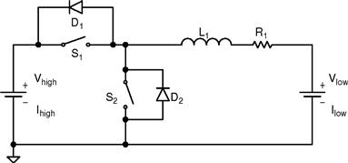
FIGURE 14.83 Switched-inductor QI and II DC/DC Luo-converter.
Mode A: The equivalent circuits during switch-on and -off periods are shown in Figs. 14.84a and b. The typical output voltage and current waveforms are shown in Fig. 14.84c.
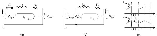
FIGURE 14.84 Mode A of F 2Q SI Luo-converter: (a) state-on: S1 on; (b) state-off: D2 on, S1, off; and (c) input and output current waveforms.
We have the average inductor current IL as
The variation ratio of the inductor current iL is
The power transfer efficiency is
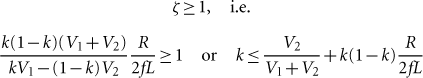
The boundary between continuous and discontinuous regions is defined as
Average inductor current IL in discontinuous region is
The power transfer efficiency is
Mode B: The equivalent circuits during switch-on and -off periods are shown in Figs. 14.85a and b. The typical output voltage and current waveforms are shown in Fig. 14.85c.
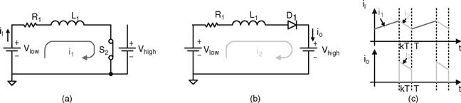
FIGURE 14.85 Mode B of F 2Q SI Luo-converter: (a) state-on: S2 on; (b) state-off: D1 on, S2 off; and (c) input and output current waveforms.
The average inductor current IL is
The variation ratio of the inductor current iL is
The power transfer efficiency
The boundary between continuous and discontinuous regions is defined as
Average inductor current Ii in discontinuous region is
The power transfer efficiency is
14.10.2 Two-quadrant Switched-inductor DC/DC Luo-converter in Reverse Operation
Reverse operation (R) 2Q SI Luo-converter is shown in Fig. 14.86, and it consists of two switches with two passive diodes, two inductors, and one capacitor. The source voltage (V1) and load voltage (V2) are usually considered as constant voltages. The load can be a battery or motor back EMF. For example, the source voltage is 42 V and load voltage is − 14 V. There are two modes of operation:
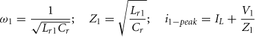
1. Mode C (QIII): electrical energy is transferred from source side V1 to load side − V2;
2. Mode D (QIV): electrical energy is transferred from load side –V2 to source side V1.
FIGURE 14.86 Switched-inductor QIII and IV DC/DC Luo-converter.
Mode C: The equivalent circuits during switch-on and -off periods are shown in Figs. 14.87a and b. The typical output voltage and current waveforms are shown in Fig. 14.87c.
FIGURE 14.87 Mode C of F 2Q SI Luo-converter: (a) state-on; S1on; (b) state-off: D2 on, S1off; and (c) input and output current waveforms.
We have the average inductor current IL as
The variation ratio of the inductor current iLis
The power transfer efficiency is
The boundary between continuous and discontinuous regions is defined as
Average inductor current IL in discontinuous region is
The power transfer efficiency is
Mode D: The equivalent circuits during switch-on and -off periods are shown in Figs. 14.88a and b. The typical output voltage and current waveforms are shown in Fig. 14.88c.
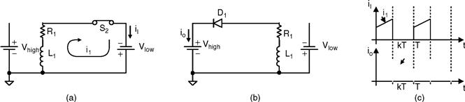
FIGURE 14.88 Mode D of F 2Q SI Luo-converter: (a) state-on: S2 on; (b) state-off: D1 on, S2 off; and (c) input and output waveforms.
The average inductor current IL is
The variation ratio of the inductor current iL is
The power transfer efficiency is
The boundary between continuous and discontinuous regions is defined as
Average inductor current IL in discontinuous region is
The power transfer efficiency is
14.10.3 Four-quadrant Switched-inductor DC/DC Luo-converter
Switched-inductor DC/DC converters successfully overcome the disadvantage of switched-capacitor converters. Usually, only one inductor is required for each converter with one-or two- or four-quadrant operation, no matter how large the difference between the input and output voltage is. Therefore, switched-inductor converter has very simple topology and circuit. Consequently, it has high power density. This paper introduces a switched-inductor four-quadrant DC/DC Luo-converter.
This converter, shown in Fig. 14.89, consists of three switches, two diodes, and only one inductor L. The source voltage V1 and load voltage V2 (e.g. a battery or DC motor back EMF) are usually constant voltages. R is the equivalent resistance of the circuit, it is usually small. In this paper, V1 > |V2|, they are supposed as + 42 V and ± 14 V, respectively. Therefore, there are four-quadrants (modes) of operation:
1. Mode A: energy is transferred from source to positive voltage load; the first-quadrant operation, QI;
2. Mode B: energy is transferred from positive voltage load to source; the second-quadrant operation, QII;
3. Mode C: energy is transferred from source to negative voltage load; the third-quadrant operation, QIII;
4. Mode C: energy is transferred from negative voltage load to source; the fourth-quadrant operation, QIV.
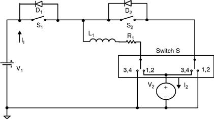
FIGURE 14.89 Four-quadrant switched-inductor DC/DC Luo-converter.
The first-quadrant is so-called the forward motoring (Forw. Mot.) operation. V1 and V2 are positive, and I1 and I2 are positive as well. The second-quadrant is so-called the forward regenerative (Forw. Reg.) braking operation. V1 and V2 are positive, and I1 and I2 are negative. The third-quadrant is so-called the reverse motoring (Rev. Mot.) operation. V1 and I1 are positive, and V2 and I2 are negative. The fourth-quadrant is so-called the reverse regenerative (Rev. Reg.) braking operation. V1 and I2 are positive, and I1 and V2 are negative. Each mode has two states: “on” and “off.” Usually, each state is operating in different conduction duty k. The switching period is T, where T = 1/f. The switch status is shown in Table 14.7.
TABLE 14.7 Switch's status (mentioned switches are not off)
Mode A is shown in Fig. 14.84. During switch-on state, switch S1 is closed. In this case the source voltage V1 supplies the load V2 and inductor L, inductor current iL increases. During switch-off state, diode D2 is on. In this case current iL flows through the load V2 via the free-wheeling diode D2, and it decreases.
Mode B is shown in Fig. 14.85. During switch-on state, switch S2 is closed. In this case the load voltage V2 supplies the inductor L, inductor current iL increases. During switch-off state, diode D1 is on, current iL flows through the source V1 and load V2 via the diode D1, and it decreases.
Mode C is shown in Fig. 14.87. During switch-on state, switch S1 is closed. The source voltage V1 supplies the inductor L, inductor current iL increases. During switch-off state, diode D2 is on. Current iL flows through the load V2 via the free-wheeling diode D2, and it decreases.
Mode D is shown in Fig. 14.88. During switch-on state, switch S2 is closed. The load voltage V2 supplies the inductor L, inductor current iL increases. During switch-off state, diode D1 is on. Current iL flows through the source V1 via the diode D1, and it decreases.
All description of the Modes A, B, C, and D is same as in Sections 14.10.1 and 14.10.2.
14.11 Multi-quadrant ZCS Quasi-resonant Luo-converters
Soft-switching converters are the fourth-generation converters. These converters are made of only inductor or capacitors. They usually perform in the systems between two voltage sources: V1 and V2. Voltage source V1 is proposed positive voltage and voltage V2 is the load voltage that can be positive or negative. In the investigation, both voltages are proposed constant voltage. Since V1 and V2 are constant value, the voltage transfer gain is constant. Our interesting research will concentrate on the working current and the power transfer efficiency η. The resistance R of the inductor has to be considered for the power transfer efficiency η calculation.
Reviewing the papers in the literature, we can find that most of the papers investigating the switched-component converters are working in single-quadrant operation. Professor Luo and colleagues have developed this technique into multi-quadrant operation. We describe these in this section and the next sections.
Multi-quadrant ZCS quasi-resonant Luo-converters are the fourth-generation converters. Because these converters implement ZCS technique, they have the advantages of high power density, high power transfer efficiency, low EMI, and reasonable EMC. They have three modes:
• Two-quadrant ZCS quasi-resonant DC/DC Luo-converter in forward operation;
• Two-quadrant ZCS quasi-resonant DC/DC Luo-converter in reverse operation;
The two-quadrant ZCS quasi-resonant DC/DC Luo-converter in forward operation is derived for the energy transmission of a dual-voltage system. Both, the source and load voltages are positive polarity. It performs in the first-quadrant QI and the second-quadrant QII corresponding to the DC motor forward operation in motoring and regenerative braking states.
The two-quadrant ZCS quasi-resonant DC/DC Luo-converter in reverse operation is derived for the energy transmission of a dual-voltage system. The source voltage is positive and load voltage is negative polarity. It performs in the third-quadrant QIII and the fourth-quadrant QIV corresponding to the DC motor reverse operation in motoring and regenerative braking states.
The four-quadrant ZCS quasi-resonant DC/DC Luo-converter is derived for the energy transmission of a dual-voltage system. The source voltage is positive, and load voltage can be positive or negative polarity. It performs four-quadrant operation corresponding to the DC motor forward and reverse operation in motoring and regenerative braking states.
14.11.1 Two-quadrant ZCS Quasi-resonant Luo-converter in Forward Operation
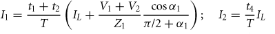
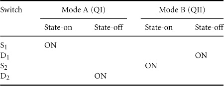
Since both voltages are low, this converter is designed as a ZCS quasi-resonant converter (ZCS-QRC). It is shown in Fig. 14.90. This converter consists of one main inductor L and two switches with their auxiliary components. A switch Sa is used for two-quadrant operation. Assuming the main inductance is sufficiently large, the current iL is constant. The source voltage V1 and load voltage V2 are usually constant, V1 = 42 V and V2 = 14 V. There are two modes of operation:
1. Mode A (Quadrant I): electrical energy is transferred from V1 side to V2 side, switch Sa links to D2;
2. Mode B (Quadrant II): electrical energy is transferred from V2 side to V1 side, switch Sa links to D1.
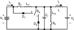
FIGURE 14.90 Two-quadrant (QI+QII) DC/DC ZCS quasi-resonant Luo-converter.
Each mode has two states: “on” and “off.” The switch status of each state is shown in Table 14.8.
TABLE 14.8 Switch's status (the blank status means off)
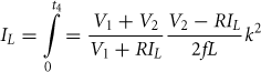
Mode A is a ZCS buck converter. The equivalent circuit, current, and voltage waveforms are shown in Fig. 14.91. There are four time regions for the switching on and off period. The conduction duty cycle is k = (t1 + t2) when the input current flows through the switch S1 and inductor L. The whole period is T = (t1 + t2 + t3 + t4). Some formulas are listed below
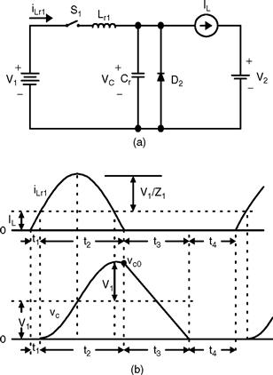
FIGURE 14.91 Mode A operation: (a) equivalent circuit and (b) waveforms.
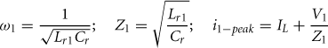
Mode B is a ZCS boost converter. The equivalent circuit, current, and voltage waveforms are shown in Fig. 14.92. There are four time regions for the switching on and off period. The conduction duty cycle is k = (t1 + t2), but the output current only flows through the source V1 in the period t4. The whole period is T = (t1 + t2 + t3 + t4). Some formulas are listed below
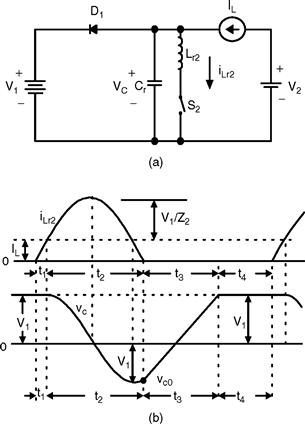
FIGURE 14.92 Mode B operation: (a) equivalent circuit and (b) waveforms.
14.11.2 Two-quadrant ZCS Quasi-resonant Luo-converter in Reverse Operation
Two-quadrant ZCS quasi-resonant Luo-converter in reverse operation is shown in Fig. 14.93. It is a new soft-switching technique with two-quadrant operation, which effectively reduces the power losses and largely increases the power transfer efficiency. It consists of one main inductor L and two switches with their auxiliary components. A switch Sa is used for two-quadrant operation. Assuming the main inductance L is sufficiently large, the current iL is constant. The source voltage V1 and load voltage V2 are usually constant, e.g. V1 = 42 V and V2 = − 28 V. There are two modes of operation:
1. Mode C (Quadrant III): electrical energy is transferred from V1 side to –V2 side, switch Sa links to D2;
2. Mode D (Quadrant IV): electrical energy is transferred from –V2 side to V1 side, switch Sa links to D1.
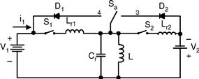
FIGURE 14.93 Two-quadrant (QIII+IV) DC/DC ZCS quasi-resonant Luo-converter.
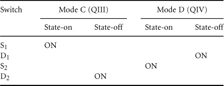
Each mode has two states: “on” and “off.” The switch status of each state is shown in Table 14.9.
TABLE 14.9 Switch's status (the blank status means off)
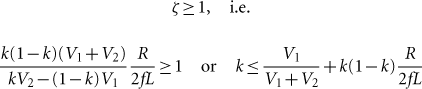
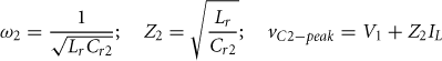
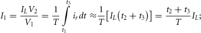
Mode C is a ZCS buck–boost converter. The equivalent circuit, current, and voltage waveforms are shown in Fig. 14.94. There are four time regions for the switching on and off period. The conduction duty cycle is kT = (t1 + t2) when the input current flows through the switch S1 and the main inductor L. The whole period is T = (t1 + t2 + t3 + t4)- Some formulas are listed below
FIGURE 14.94 Mode C operation: (a) equivalent circuit and (b) waveforms.
Mode D is a cross ZCS buck–boost converter. The equivalent circuit, current, and voltage waveforms are shown in Fig. 14.95. There are four time regions for the switching on and off period. The conduction duty cycle is kT = (t1 + t2), but the output current only flows through the source V1 in the period t4. The whole period is T = (t1 + t2 + t3 + t4). Some formulas are listed below
FIGURE 14.95 Mode D operation: (a) equivalent circuit and (b) waveforms.
14.11.3 Four-quadrant ZCS Quasi-resonant Luo-converter
Four-quadrant ZCS quasi-resonant Luo-converter is shown in Fig. 14.96. Circuit 1 implements the operation in quadrants I and II, circuit 2 implements the operation in quadrants III and IV. Circuit 1 and 2 can be converted to each other by auxiliary switch. Each circuit consists of one main inductor L and two switches. A switch Sa is used for four-quadrant operation. Assuming that the main inductance L is sufficiently large, the current iL remains constant. The source and load voltages are usually constant, e.g. V1 = 42 V and V2 = ± 28 V [7–9]. There are four modes of operation:
1. Mode A (Quadrant I): electrical energy is transferred from V1 side to V2 side, switch Sa links to D2;
2. Mode B (Quadrant II): electrical energy is transferred from V2 side to V1 side, switch Sa links to D1;
3. Mode C (Quadrant III): electrical energy is transferred from V1 side to - V2 side, switch Sa links to D2;
4. Mode D (Quadrant IV): electrical energy is transferred from –V2 side to V1 side, switch Sa links to D1.
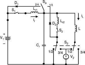
FIGURE 14.96 Four-quadrant DC/DC ZCS quasi-resonant Luo-converter.
Each mode has two states: “on” and “off.” The switch status of each state is shown in Table 14.10.
TABLE 14.10 Switch's status (the blank status means off)
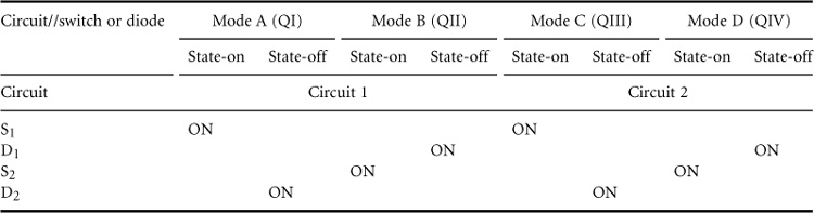
The operation of Mode A, B, C, and D is same as in the previous Sections 14.11.1 and 14.11.2.
14.12 Multi-quadrant ZVS Quasi-resonant Luo-converters
Multi-quadrant ZVS quasi-resonant Luo-converters are the fourth-generation converters. Because these converters implement ZCS technique, they have the advantages of high power density, high power transfer efficiency, low EMI, and reasonable EMC. They have three modes:
• Two-quadrant ZVS quasi-resonant DC/DC Luo-converter in forward operation;
• Two-quadrant ZVS quasi-resonant DC/DC Luo-converter in reverse operation;
The two-quadrant ZVS quasi-resonant DC/DC Luo-converter in forward operation is derived for the energy transmission of a dual-voltage system. Both, the source and load voltages are positive polarity. It performs in the first-quadrant QI and the second-quadrant QII corresponding to the DC motor forward operation in motoring and regenerative braking states.
The two-quadrant ZVS quasi-resonant DC/DC Luo-converter in reverse operation is derived for the energy transmission of a dual-voltage system. The source voltage is positive and load voltage is negative polarity. It performs in the third-quadrant QIII and the fourth-quadrant QIV corresponding to the DC motor reverse operation in motoring and regenerative braking states.
The four-quadrant ZVS quasi-resonant DC/DC Luo-converter is derived for the energy transmission of a dual-voltage system. The source voltage is positive, and load voltage can be positive or negative polarity. It performs four-quadrant operation corresponding to the DC motor forward and reverse operation in motoring and regenerative braking states.
14.12.1 Two-quadrant ZVS Quasi-resonant DC/DC Luo-converter in Forward Operation
Two-quadrant ZVS quasi-resonant Luo-converter in forward operation is shown in Fig. 14.97. It consists of one main inductor L and two switches with their auxiliary components.

FIGURE 14.97 Two-quadrant (QI+QII) DC/DC ZVS quasi-resonant Luo-converter.
Assuming the main inductance L is sufficiently large, the current iL is constant. The source voltage V1 and load voltage V2 are usually constant, e.g. V1 = 42 V and V2 = 14 V. There are two modes of operation:
1. Mode A (Quadrant I): electrical energy is transferred from V1 side to V2 side;
2. Mode B (Quadrant II): electrical energy is transferred from V2 side to V1 side.
Each mode has two states: “on” and “off.” The switch status of each state is shown in Table 14.11.
TABLE 14.11 Switch's status (the blank status means off)
Mode A is a ZVS buck converter shown in Fig. 14.98. There are four time regions for the switching on and off period. The conduction duty cycle is kT = (t3 + t4) when the input current flows through the switch S1 and the main inductor L. The whole period is T = (t1 + t2 + t3 + t4). Some relevant formulas are listed below
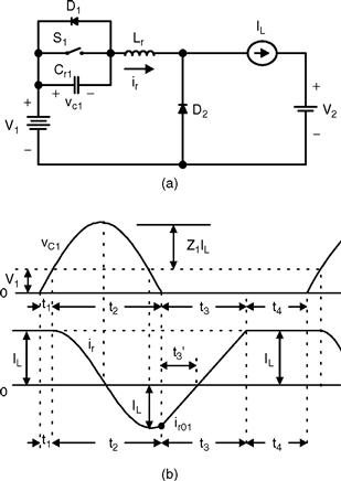
FIGURE 14.98 Mode A operation: (a) equivalent circuit and (b) waveforms.
 (14.346)
Mode B is a ZVS boost converter shown in Fig. 14.99. There are four time regions for the switching on and off period. The conduction duty cycle is kT = (t3 + t4), but the output current only flows through the source V1 in the period (t1 + t2). The whole period is T = (t1 + t2 + t3 + t4). Some relevant formulas are listed below
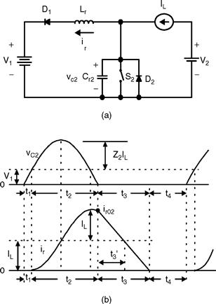
FIGURE 14.99 Mode B operation: (a) equivalent circuit and (b) waveforms.
14.12.2 Two-quadrant ZVS Quasi-resonant DC/DC Luo-converter in Reverse Operation
Two-quadrant ZVS quasi-resonant Luo-converter in reverse operation is shown in Fig. 14.100. It consists of one main inductor L and two switches with their auxiliary components. Assuming the main inductance L is sufficiently large, the current iL is constant. The source voltage V1 and load voltage V2 are usually constant, e.g. V1 = + 42 V and V2 = − 28 V. There are two modes of operation:
1. Mode C (Quadrant III): electrical energy is transferred from V1 side to –V2 side;
2. Mode D (Quadrant IV): electrical energy is transferred from –V2 side to V1 side.
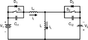
FIGURE 14.100 Two-quadrant (QIII+IV) DC/DC ZVS quasi-resonant Luo-converter.
Each mode has two states: “on” and “off.” The switch status of each state is shown in Table 14.12.
TABLE 14.12 Switch's status (the blank status means off)
Mode C is a ZVS buck–boost converter shown in Fig. 14.101. There are four time regions for the switching on and off period. The conduction duty cycle is kT = (t3 + t4) when the input current flows through the switch S1 and the main inductor L. The whole period is T = (t1 + t2 + t4 + t4).
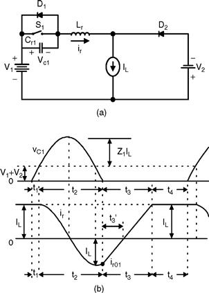
FIGURE 14.101 Mode C operation: (a) equivalent circuit and (b) waveforms.
Some formulas are listed below
Mode D is a cross ZVS buck–boost converter shown in Fig. 14.102. There are four time regions for the switching on and off period. The conduction duty cycle is kT = (t3 + t4), but the output current only flows through the source V1 in the period (t1 + t2). The whole period is T = (t1 + t2 + t3 + t4). Some formulae are listed below
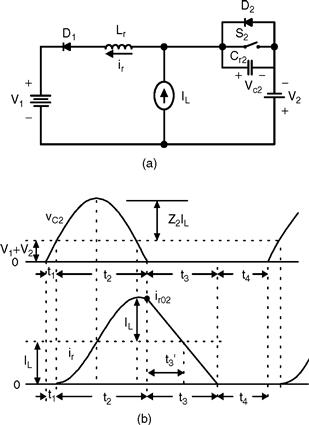
FIGURE 14.102 Mode D operation: (a) equivalent circuit and (b) waveforms.
![]() (14.363)
(14.363)
14.12.3 Four-quadrant ZVS Quasi-resonant DC/DC Luo-converter
Four-quadrant ZVS quasi-resonant Luo-converter is shown in Fig. 14.103. Circuit 1 implements the operation in quadrants I and II, circuit 2 implements the operation in quadrants III and IV. Circuit 1 and 2 can be converted to each other by auxiliary switch. Each circuit consists of one main inductor L and two switches. Assuming that the main inductance L is sufficiently large, the current iL is constant. The source and load voltages are usually constant, e.g. V1 = 42 V and V2 = ± 28 V.
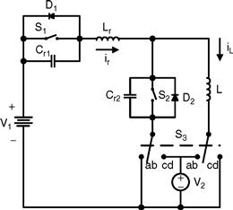
FIGURE 14.103 Four-quadrant DC/DC ZVS quasi-resonant Luo-converter.
There are four modes of operation:
• Mode A (Quadrant I): electrical energy is transferred from V1 side to V2 side;
• Mode B (Quadrant II): electrical energy is transferred from V2 side to V1 side;
• Mode C (Quadrant III): electrical energy is transferred from V1 side to –V2 side;
• Mode D (Quadrant IV): electrical energy is transferred from –V2 side to V1 side.
Each mode has two states: “on” and “off.” The switch status of each state is shown in Table 14.13.
TABLE 14.13 Switch's status (the blank status means off)
The description of Modes A, B, C, and D is same as in the previous Sections 14.12.1 and 14.12.2.
14.13 Synchronous-rectifier DC/DC Luo-converters
Synchronous-rectifier (SR) DC/DC converters are called the fifth-generation converters. The development of the microelectronics and computer science requires the power supplies with low output voltage and strong current. Traditional diode bridge rectifiers are not available for this requirement. Softswitching technique can be applied in SR DC/DC converters. We have created few converters with very low voltage (5 V, 3.3 V, and 1.8 ~ 1.5 V) and strong current (30 A, 60 A up to 200 A) and high power transfer efficiency (86%, 90% up to 93%). In this section, few new circuits, different from the ordinary SR DC/DC converters, are introduced:
• Flat transformer synchronous-rectifier DC/DC Luo-converter;
• Double current synchronous-rectifier DC/DC Luo-converter with active clamp circuit;
• Zero-current-switching synchronous-rectifier DC/DC Luo-converter;
• Zero-voltage-switching synchronous-rectifier DC/DC Luo-converter.
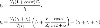
14.13.1 Flat Transformer Synchronous-rectifier DC/DC Luo-converter
Flat transformer SR DC/DC Luo-converter is shown in Fig. 14.104. The switches S1, S2, and S3 are the low-resistance MOSFET devices with very low resistance Rs (7-8 mΩ). Since we use a flat transformer, the leakage inductance Lm and resistance RL are small. Other parameters are C = 1 μF, Lm = 1 nH, RL = 2 mΩ, L = 5 μΩ, Co = 10 μF. The input voltage is V1 = 30VDC and output voltage is V2, the output current is IO. The transformer term's ratio is N = 12: 1. The repeating period is T = 1/f and conduction duty is k. There are four working modes.
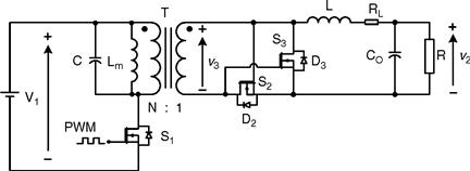
FIGURE 14.104 Flat transformer SR Luo-converter.
The natural resonant frequency is
![]() (14.367)
(14.367)
The intervals are
![]() (14.368)
(14.368)
 (14.369)
Average output voltage V2 and input current I1 are
![]() (14.370)
(14.370)
The power transfer efficiency is
![]() (14.371)
(14.371)
When we set the frequency f = 150–200 kHz, we obtained the V2 = 1.8V, N=12, I? = 0–30 A, Volume = 2.5in3. The average power transfer efficiency is 92.3% and the maximum power density (PD) is 21.6 W/in3.
14.13.2 Double Current SR DC/DC Luo-converter with Active Clamp Circuit
The converter in Fig. 14.104 resembles a half-wave rectifier. Double current (DC) SR DC/DC Luo-converter with active clamp circuit is shown in Fig. 14.105. The switches S1–S4 are the low-resistance MOSFET devices with very low resistance RS (7–8 mΩ). Since S3 and S4 plus L1 and L2 form a double current circuit and S2 plus C is the active clamp circuit, this converter resembles a full-wave rectifier and obtains strong output current. Other parameters are C = 1 μF, Lm = 1 nH, RL = 2mΩ, L = 5 μH, CO = 10 μF. The input voltage is V1 = 30VDC and output voltage is V2, the output current is I?. The transformer term's ratio is N = 12: 1. The repeating period is T = 1/f and conduction duty is k. There are four working modes.
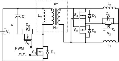
FIGURE 14.105 Double current SR Luo-converter.
The natural resonant frequency is
![]() (14.372)
(14.372)
The interval of t1 is
![]() (14.373)
(14.373)
 (14.374)
Average output voltage V2 and input current I1 are
![]() (14.375)
(14.375)
The power transfer efficiency
![]() (14.376)
(14.376)
When we set the frequency f = 200–250kHz, we obtained the V2 = 1.8V, N = 12,1? = 0–35 A, Volume = 2.5 in3. The average power transfer efficiency is 94% and the maximum power density (PD) is 25 W/in3.
14.13.3 Zero-current-switching Synchronous-rectifier DC/DC Luo-converter
Since the power loss across the main switch S1 is high in DC SR DC/DC Luo-converter, we designed ZCS SR DC/DC Luo-converter shown in Fig. 14.106. This converter is based on the DC SR DC/DC Luo-converter plus ZCS technique. It employs a double core flat transformer.
FIGURE 14.106 ZCS DC SR Luo-converter.
The ZCS resonant frequency is
![]() (14.377)
(14.377)
The normalized impedance is
 (14.378)
The intervals are
![]() (14.379)
(14.379)
 (14.380)
Average output voltage V2 and input current I1 are
![]() (14.381)
(14.381)
The power transfer efficiency
![]() (14.382)
(14.382)
When we set the V1 = 60 V and frequency f = 200–250 kHz, we obtained the V2 = 1.8 V, N = 12, Io = 0–60 A, Volume = 4in3. The average power transfer efficiency is 94.5% and the maximum power density (PD) is 27 W/in3.
14.13.4 Zero-voltage-switching Synchronous-rectifier DC/DC Luo-converter
ZVS SR DC/DC Luo-converter is shown in Fig. 14.107. This converter is based on the DC SR DC/DC Luo-converter plus ZVS technique. It employs a double core flat transformer.
FIGURE 14.107 ZVS DC SR Luo-converter.
The ZVS resonant frequency is
![]() (14.383)
(14.383)
 (14.384)
The intervals are
![]() (14.385)
(14.385)
![]() (14.386)
(14.386)
Average output voltage V2 and input current I1 are
![]() (14.387)
(14.387)
The power transfer efficiency
![]() (14.388)
(14.388)
When we set the V1 = 60 V and frequency f= 200–250 kHz, we obtained the V2 = 1.8 V, N = 12, I? = 0–60 A, Volume = 4 in3. The average power transfer efficiency is 94.5% and the maximum power density (PD) is 27 W/in3.
14.14 Multiple-element Resonant Power Converters
Multiple energy-storage elements resonant power converters (x-Element RPC) are the sixth-generation converters. According to the transferring, power becomes higher and higher, traditional methods are hardly satisfied to deliver large power from source to final actuators with high efficiency. In order to reduce the power losses during the conversion process the sixth-generation converters –multiple energy-storage elements resonant power converters (x-Element RPC) –are created. They can be sorted into two main groups:
• DC/DC resonant converters;
• DC/AC resonant inverters.
Both groups converters consist of multiple energy-storage elements: two elements, three elements, or four elements. These energy-storage elements are passive parts: inductors and capacitors. They can be connected in series or parallel in various methods. In full statistics, the circuits of the multiple energy-storage elements converters are:
• 8 topologies of 2-element RPC;
• 38 topologies of 3-element RPC;
• 98 topologies of 4-element (2L-2C) RPC.
How to investigate the large quantity converters is a vital task. This problem was addressed in the last decade of last century. Unfortunately, much attention was not paid to it. This generation converters were not well discussed, only limited number of papers was published in the literature.
14.14.1 Two Energy-storage Elements Resonant Power Converters
The 8 topologies of 2-element RPC are shown in Fig. 14.108. These topologies have simple circuit structure and least components. Consequently, they can transfer the power from source to end-users with higher power efficiency and lower power losses.
FIGURE 14.108 8 topologies of 2-element RPC.
Usually, the 2-Element RPC has very narrow response frequency bands, which is defined as the frequency width between the two half-power points. The working point must be selected in the vicinity of the natural resonant frequency ![]() . Another drawback is that the transferred waveform is usually not a perfect sinusoidal, i.e. the output waveform THD is not zero.
. Another drawback is that the transferred waveform is usually not a perfect sinusoidal, i.e. the output waveform THD is not zero.
Since total power losses are mainly contributed by the power losses across the main switches. As resonant conversion technique, the 2-Element RPC has high power transferring efficiency.
14.14.2 Three Energy-storage Elements Resonant Power Converters
The 38 topologies of 3-element RPC are shown in Fig. 14.109. These topologies have one more component when compared to the 2-element RPC topologies. Consequently, they can transfer the power from source to end-users with higher lower power and lower power transfer efficiency.
FIGURE 14.109 38 topologies of 3-element RPC.
Usually, the 3-element RPC has a much wider response frequency bands, which is defined as the frequency width between the two half-power points. If the circuit is a low-pass filter, the frequency bands can cover the frequency range from 0 to the natural resonant frequency ![]() . The working point can be selected from a much wider frequency width which is lower than the natural resonant frequency
. The working point can be selected from a much wider frequency width which is lower than the natural resonant frequency ![]() .
.
Another advantage, better than the 2-element RPC topologies, is that the transferred waveform can usually be a perfect sinusoidal, i.e. the output waveform THD is nearly zero. As well-known, mono-frequency waveform transferring operation has very low EMI.
14.14.3 Four Energy-storage Elements Resonant Power Converters
The 98 topologies of 4-element (2L-2C) RPC are shown in Fig. 14.110. If no restriction such as 2L-2Cfor 4-element RPC, the number of the topologies of 4-element RPC can be much larger. Although these topologies have comparably complex circuit structure, they can still transfer the power from source to end-users with higher power efficiency and lower power losses.
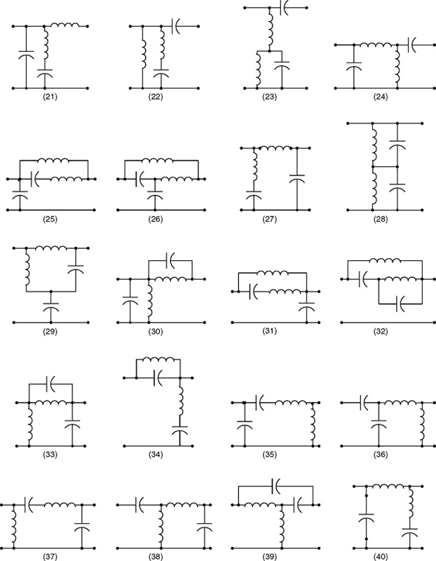
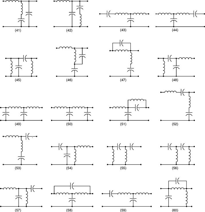
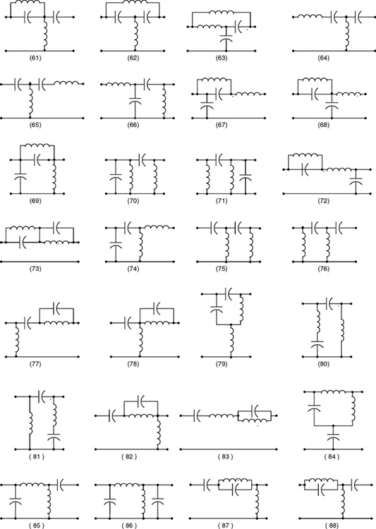
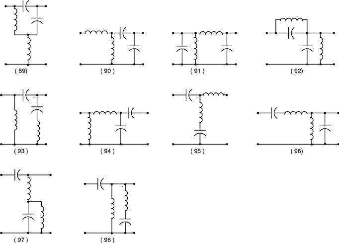
FIGURE 14.110 98 topologies of 4-element RPC.
Usually, the 4-element RPC has a wide response frequency bands, which is defined as the frequency width between the two half-power points. If the circuit is a low-pass filter, the frequency bands can cover the frequency range from 0 to the high half-power point which is definitely higher that the natural resonant frequency ![]() . The working point can be selected from a wide area across (lower and higher than) the natural resonant frequency
. The working point can be selected from a wide area across (lower and higher than) the natural resonant frequency ![]() . Another advantage is that the transferred waveform is usually a perfect sinusoidal, i.e. the output waveform THD is very close to zero. As well-known, mono-frequency-waveform transferring operation has very low EMI and reasonable EMS and EMC.
. Another advantage is that the transferred waveform is usually a perfect sinusoidal, i.e. the output waveform THD is very close to zero. As well-known, mono-frequency-waveform transferring operation has very low EMI and reasonable EMS and EMC.
14.14.4 Bipolar Current and Voltage Sources
Depending on different applications, resonant network can be low-pass filter, high-pass filter, or band-pass filter. For large power transferring, low-pass filter is usually employed. In this case, inductors are arranged in series arms and capacitors are arranged in shunt arms. If the first component is inductor, only voltage source can be applied since inductor current is continuous. Vice versa, if the first component is capacitor, only current source can be applied since capacitor voltage is continuous.
14.14.4.1 Bipolar Voltage Source
A bipolar voltage source using single voltage source is shown in Fig. 14.111. Since only voltage source is applied, there are four switches applied alternatively switching on or off to supply positive and negative voltage to the network. In the figure, the load is a resistance R.
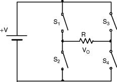
FIGURE 14.111 A bipolar voltage source using single voltage source.
The circuit of this voltage source is likely a four-quadrant operational chopper. The conduction duty cycle for each switch is 50%. For safety reason, the particular circuitry design has to consider some small gap between the turnover (commutation) operation to avoid the short-circuit incidence.
The repeating frequency is theoretically not restricted. For industrial applications, the operating frequency is usually arranged in the range between 10 kHz and 5 MHz, depending on the application conditions.
14.14.4.2 Bipolar Current Source
A bipolar current voltage source using single voltage sources is shown in Fig. 14.112. To obtain stable current, the voltage source is connected in series by a large inductor. There are four switches applied alternatively switching on or off to supply positive and negative current to the network. In the figure, the load is a resistance R.
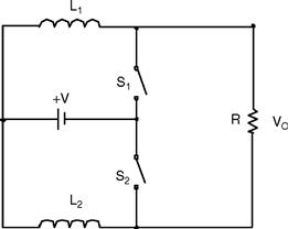
FIGURE 14.112 A bipolar current voltage source using single voltage source.
The circuit of this current source is likely a two-quadrant operational chopper. The conduction duty cycle for each switch is 50%. For safety reason, the particular circuitry design has to consider some small gap between the turnover (commutation) operation to avoid the short-circuit incidence.
The repeating frequency is theoretically not restricted. For industrial applications, the operating frequency is usually arranged in the range between 10 kHz and 5 MHz, depending on the application conditions.
14.15 Gate Control Luo-resonator
Luo-resonator is shown in Fig. 14.113. It generates the PWM pulse train to drive the static switch S. Luo-resonator is a high efficiency and simple structure circuit with easily adjusting frequency f and conduction duty k. It consists of three operational amplifiers (OA) named OA1–3 and auxiliary. These three 741-type OA's are integrated in a chip TL074 (which contains four OA,s). Two potentiometers are applied to adjust the frequency f and conduction duty k. The voltage waveforms are shown in Fig. 14.114.
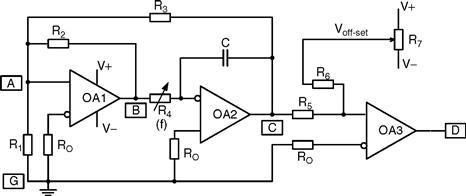
FIGURE 14.113 Luo-resonator.
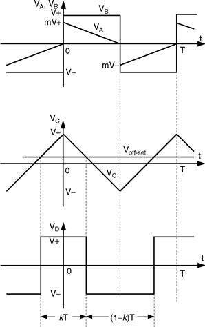
FIGURE 14.114 Voltage waveforms of Luo-resonator.
Type-741 OA can work at the power supply ± 3 –± 18V that are marked V+, G, and V- with |V –| = V+. OA2 in Fig. 14.113 acts as the integration operation, its output VC is a triangle waveform with regulated frequency f = 1/T controlled by potentiometer R4. OA1 acts as a resonant operation, its output VB is a square-waveform with the frequency f. OA3 acts as a comparator, its output Vd is a square-waveform pulse train with regulated conduction duty k controlled by R7.
Firstly, assuming the voltage VB = V+ at t = 0 and feeds positively back to OA1 via R2. This causes the OAl's output voltage maintained at VB = V+. In the meantime, VB inputs to OA2 via R4, the output voltage VC of OA2, therefore, decreases towards V– with the slope 1/R4C. Voltage VC feeds negatively back to OA1 via R3. Voltage VA at point A changes from (mV+) to 0 in the period of 2 mR4 C. Usually, R3 is set slightly smaller than R2, the ratio is defined as m = -R3/R2. Thus, voltage VA intends towards negative. It causes the OAl's output voltage VB = V– at t = 2m R4 C and voltage VA jumps to m V–. Vice versa, the voltage VB = V– at t = 2 mR4 C and feeds positively back to OA1 via R2. This causes the OAl's output voltage maintained at VB = V–. In the meantime, VB inputs to OA2 via R4, the output voltage VC of OA2, therefore, increases towards V+ with the slope 1/R4 C. Voltage VC feeds negatively back to OA1 via R3. Voltage Va at point A changes from (mV –) to 0 in the period of 2mR4 C. Thus, voltage Va intends towards positive. It causes the OAl's output voltage VB = V+ at t = 4mR4 C and voltage Va jumps to mV+.
Then VC inputs to OA3 and compares with shift signal Voff-set regulated by the potentiometer R7 via R6. When Voff-set = 0, OA3 yields its output voltage Vd as a pulse train with conduction duty k = 0.5. Positive Voff-set shifts the zero-cross point of voltage VC downwards, hence, OA3 yields its output voltage Vd as a pulse train with conduction duty k > 0.5. Vice versa, negative Voff-set shifts the zero-cross point of voltage VC upwards, hence, OA3 yields its output voltage Vd as a pulse train with conduction duty k < 0.5 as shown in Fig. 14.114. Conduction duty k is controlled by Voff-set via the potentiometer R7.
The calculation formulas are
![]() (14.389)
(14.389)
![]() (14.390)
(14.390)
![]() (14.391)
(14.391)
This PWM pulse train Vd is applied to the DC/DC converter switch such as a transistor, MOSFET, or IGBT via a coupling circuit.
A design example: A Luo-resonator was designed as shown in Fig. 14.113 with the component values of R0 = 10 kΩ; R1 = R2 = R5 = 100 kΩ, R3 = R6 = 95 kΩ; R4 = 510 Ω–5.1 kΩ R7 = 20 kΩ; and C = 5.1 n F. The results are m = 0.95, frequency f = 10–100 kHz and conduction duty k = 0–1.0.
14.16 Applications
The DC/DC conversion technique has been rapidly developed and has been widely applied in industrial applications and computer peripheral equipment. Three examples are listed below:
• 5000 V insulation test bench;
• MIT 42/14 V DC/DC converter;
• IBM 1.8 V/200 A power supply.
14.16.1 5000 V Insulation Test Bench
Insulation test bench is the necessary equipment for semiconductor manufacturing organizations. An adjustable DC voltage power supply is the heart of this equipment. Traditional method to obtain the adjustable high DC voltage is a diode rectifier via a setting up transformer. It is costly and larger in size with poor efficiency.
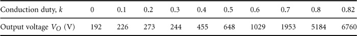
Using a positive output super-lift Luo -converter triple-lift circuit, which is shown in Fig. 14.115. This circuit is small, effective, and low cost. The output voltage can be determined by
![]() (14.392)
(14.392)
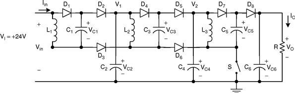
FIGURE 14.115 5000 V Insulation test bench.
The conduction duty cycle k is only adjusted in the range 0–0.8 to carry out the output voltage in the range of 192–5184 V.
The experimental results are listed in Table 14.14. The measured data verified the advantages of this power supply.
TABLE 14.14 The experimental results of the 5000 V test bench
14.16.2 MIT 42/14 V–3 KW DC/DC Converter
MIT 42/14 V-3 KW DC/DC converter was requested to transfer 3 kW energy between two battery sources with 42 and 14 V. The circuit diagram is shown in Fig. 14.116. This is a two-quadrant zero-voltage-switching (ZVS) quasi-resonant-converter (QRC). The current in low voltage side can be up to 250 A. This is a typical low voltage strong current converter. It is easier to carry out by ZVS-QRC.
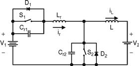
FIGURE 14.116 MIT 42/14 V-3 kW DC/DC converter.
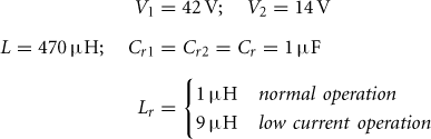
This converter consists of two sources V1 and V2, one main inductor L, two main switches S1 and S2, two reverse-paralleled diodes D1 and D2, one resonant inductor Lr and two resonant capacitors Cr1 and Cr2. The working condition is selected
Therefore,
![]() (14.393)
(14.393)
 (14.394)
![]() (14.395)
(14.395)
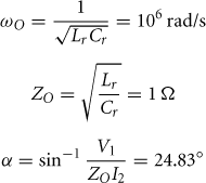
It is easy to keep the quasi-resonance when the working current I2 > 50 A. If the working current is too low, the resonant inductor will take large value to guarantee the quasi-resonance state. This converter performs two-quadrant operation:
• Mode A (Quadrant I): energy transferred from V1 side to V2 side;
• Mode B (Quadrant II): energy transferred from V2 side to V1 side.
Assuming the working current is I2 = 100 A and the converter works in Mode A, following calculations are obtained
 (14.396)
![]() (14.397)
(14.397)
![]() (14.398)
(14.398)
![]() (14.399)
(14.399)
![]() (14.400)
(14.400)
![]() (14.401)
(14.401)
![]() (14.402)
(14.402)
![]() (14.403)
(14.403)
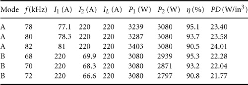
The volume of this converter is 270in3. The experimental test results in full power 3kW are listed in Table 14.15. From the tested data, a high power density 22.85 W/in3 and a high efficiency 93% are obtained. Because of soft-switching operation, the EMI is low and EMS and EMC are reasonable.
TABLE 14.15 The experimental test results of MIT 42V/14 converter (with the condition: Lr = 1 μ,H, Cr1 = Cr2 = 1 μF)
14.16.3 IBM 1.8 V/200 A Power Supply
This equipment is suitable for IBM new generation computer with power supply 1.8 V/200 A. This is a ZCS SR DC/DC Luo-converter, and is shown in Fig. 14.117. This converter is based on the double-current synchronous-rectifier DC/DC converter plus ZCS technique. It employs a hixaploid-core flat-transformer with the turns ratio N = 1/12. It has six-unit ZCS synchronous-rectifier double-current DC/DC converter. The six primary coils are connected in series, and six secondary circuits are connected in parallel. Each unit has particular input voltage Vin to be about 33 V, and can offer 1.8 V/35 A individually. Total output current is 210 A. The equivalent primary full current is I1 = 14.5 A and equivalent primary load voltage is V2 = 200 V. The ZCS natural resonant frequency is
![]() (14.404)
(14.404)
 (14.405)
![]() (14.406)
(14.406)
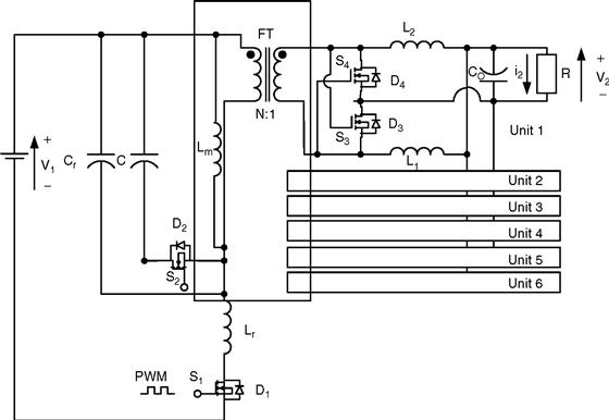
FIGURE 14.117 IBM 1.8 V/200 A power supply.
The main power supply is from public utility board (PUB) via a diode rectifier. Therefore V1 is nearly 200 V, and the each unit input voltage Vin is about 33 V. Other calculation formulas are
![]() (14.407)
(14.407)
![]() (14.408)
(14.408)
![]() (14.409)
(14.409)
![]() (14.410)
(14.410)
![]() (14.411)
(14.411)
![]() (14.412)
(14.412)
![]() (14.413)
(14.413)
Real output voltage and input current are
![]() (14.414)
(14.414)
![]() (14.415)
(14.415)
The efficiency is
![]() (14.416)
(14.416)
The commercial unit of this power supply works in voltage closed loop control with inner current closed loop to keep the output voltage constant. Applying frequency is arranged in the band of 200–250 kHz. Whole volume of the power supply is 14in3. The transfer efficiency is about 88–92% and power density is about 25.7 W/in3.
14.17 Energy Factor and Mathematical Modeling for Power DC/DC Converters
We have well discussed the various DC/DC converters operating in steady state in previous sections. We will investigate the transient process of DC/DC converters. Furthermore, we define a series of new parameters such as energy factor (EF) and so on to establish the mathematical modeling of all power DC/DC converters.
Energy storage in power DC/DC converters has been paid attention long time ago. Unfortunately, there is no clear concept to describe the phenomena and reveal the relationship between the stored energy and the characteristics of power DC/DC converters. We have theoretically defined a new concept –energy factor (EF) and researched the relations between EF and the mathematical modeling of power DC/DC converters. Energy factor is a new concept in power electronics and conversion technology, which thoroughly differs from the traditional concepts such as power factor (PF), power transfer efficiency (η), total harmonic distortion (THD), and ripple factor (RF). Energy factor and the other sub-sequential parameters can illustrate the system stability, reference response, and interference recovery. This investigation is very helpful for system design and DC/DC converters characteristics foreseeing.
14.17.1 Pumping Energy (PE)
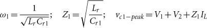
All power DC/DC converters have pumping circuit to transfer the energy from the source to some energy storage passive elements, e.g. inductors and capacitors. The PE is used to count the input energy in a switching period T. Its calculation formula is
![]() (14.417)
(14.417)
where
![]()
is the average value of the input current if the input voltage V1 is constant. Usually the input average current I1 depends on the conduction duty cycle.
14.17.2 Stored Energy (SE)
The stored energy in an inductor is
![]() (14.418)
(14.418)
The stored energy across a capacitor is
![]() (14.419)
(14.419)
Therefore, if there are nL, inductors and nC capacitors the total stored energy in a DC/DC converter is
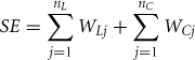 (14.420)
Capacitor–inductor stored energy ratio(CIR) – Most power DC/DC converters consist of inductors and capacitors.
Therefore, we can define the capacitor-inductor stored energy ratio (CIR).
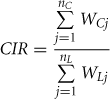 (14.421)
Energy losses (EL) – Usually, most analysis applied in DC/DC converters is assuming no power losses, i.e. the input power is equal to the output power, Pin = P0 or V1 I1 = V2 I2, so that pumping energy is equal to output energy in a period, T.
Particularly, power losses always exist during the conversion process. They are caused by the resistance of the connection cables, resistance of the inductor and capacitor wire, and power losses across the semiconductor devices (diode, IGBT, MOSFET, and so on). We can sort them as the resistance power losses Pr, passive element power losses Pe, and device power losses Pd. The total power losses are Ploss.
![]()
and
![]()
Therefore,
![]()
The energy losses ( EL ) is in a period T,
![]() (14.422)
(14.422)
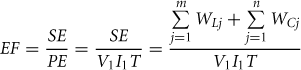
14.17.3 Energy Factor (EF)
As described in previous section the input energy in a period T is the pumping energy PE = Pin × T = VinIin × T. We now define the EF, that is the ratio of the SE over the pumping energy
 (14.423)
Energy factor is a very important factor of a power DC/DC converter. It is usually independent from the conduction duty cycle k, and proportional to the switching frequency f (inversely proportional to the period T) since the pumping energy PE is proportional to the switching period T.
14.17.4 Time Constant τ and Damping Time Constant τd
The time constant τ of a power DC/DC converter is a new concept to describe the transient process of a DC/DC converter. If no power losses in the converter, it is defined
![]() (14.424)
(14.424)
The damping time constant τd of a power DC/DC converter is new concept to describe the transient process of a DC/DC converter. If no power losses, it is defined
![]() (14.425)
(14.425)
The time constants ratio τ of a power DC/DC converter is new concept to describe the transient process of a DC/DC converter. If no power losses, it is defined
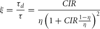 (14.426)
14.17.5 Mathematical Modeling for Power DC/DC Converters
The mathematical modeling for all power DC/DC converters is
![]() (14.427)
(14.427)
where M is the voltage transfer gain: M = Vo/Vin, τ is the time constant in Eq. (14.424), τd the damping time constant in Eq. (14.425), τd = ττ. Using this mathematical model of power DC/DC converters, it is significantly easy to describe the characteristics of power DC/DC converters. In order to verify this theory, few converters are investigated to demonstrate the characteristics of power DC/DC converters and applications of the theory.
14.17.6 Buck Converter with Small Energy Losses (rL= 1.5 Ω)
A buck converter shown in Fig. 14.118 has the components values: V1 = 40 V, L = 250 μH with resistance rL = 1.5 Ω, C = 60 μF, R = 10 Ω, the switching frequency f = 20 kHz (T = 1/f = 50 µs) and conduction duty cycle k = 0.4. This converter is stable and works in CCM.
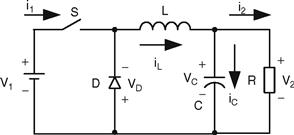
FIGURE 14.118 A buck converter.
Therefore, we have got the voltage transfer gain M = 0.35, i.e. V2 = VC = MV1 = 0.35 × 40 = 14V. IL = I2 = 1.4A, Ploss = I2L × rL= 1.42 × 1.5 = 2.94 W, and I1 = 0.564A. The parameter EF and others are listed below
![]()
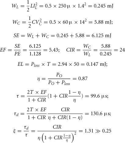
By cybernetic theory, since the damping time constant τd is larger than the time constant τ, the corresponding ratio τ is 1.31 ![]() 0.25. The output voltage has heavy oscillation with high overshot. The corresponding transfer function is
0.25. The output voltage has heavy oscillation with high overshot. The corresponding transfer function is
![]() (14.428)
(14.428)
where
![]()
with
![]()
and
![]()
The unit-step function response is
![]() (14.429)
(14.429)
The unit-step function response (transient process) has oscillation progress with damping factor σ and frequency ω. The simulation result is shown in Fig. 14.119.
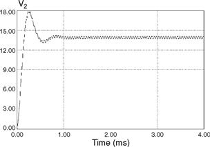
FIGURE 14.119 Buck converter unit-step response.
The impulse interference response is
![]()
where U is the interference signal. The impulse response (interference recovery process) has oscillation progress with damping factor σ and frequency ω. The simulation result is shown in Fig. 14.120.
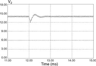
FIGURE 14.120 Buck converter impulse response.
In order to verity the analysis, calculation and simulation results, we constructed a test rig with same conditions. The corresponding experimental results are shown in Figs. 14.121 and 14.122.
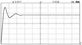
FIGURE 14.121 Unit-step response (test).
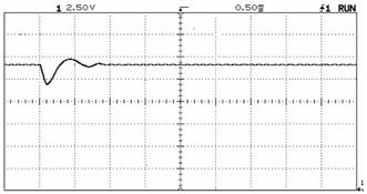
FIGURE 14.122 Impulse response (test).
14.17.7 A Super-lift Luo-converter in CCM
Figure 14.123 shows a super-lift Luo-converter with the conduction duty k = 0.5. The components values are V1 = 20 V, f = 50 kHz (T = 20 µs), L = 100 μH with resistance rL = 0.12 Ω, C1 = 2500 µF, C2 = 800 µ F, and R = 10 Ω. This converter is stable and works in CCM.
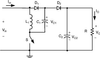
FIGURE 14.123 A super-lift Luo-converter.
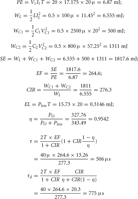
Therefore, we have got the voltage transfer gain M = 2.863, i.e. the output voltage V2 = VC2 = 57.25 V. VC1 = V1 = 20 V, I1 = 14.145A, I2 = 5.725A, IL = 11.45A, and Ploss = I2L × rL = 11.452 × 0.12 = 15.73 W. The parameter EF and others are listed below
By cybernetic theory, since the damping time constant τd is much larger than the time constant τ, the corresponding ratio τ = 775/506 = 1.53 ![]() 0.25. The output voltage has heavy oscillation with high overshot. The transfer function of this converter has two poles (–s1 and –s2) that are located in the left-hand half plane (LHHP).
0.25. The output voltage has heavy oscillation with high overshot. The transfer function of this converter has two poles (–s1 and –s2) that are located in the left-hand half plane (LHHP).
where
with
The unit-step function response is
The unit-step function response (transient process) has oscillation progress with damping factor σ and frequency ω. The simulation is shown in Fig. 14.124.
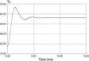
FIGURE 14.124 SL Luo-converter unit-step response.
The impulse interference response is
where U is the interference signal. The impulse response (interference recovery process) has oscillation progress with damping factor σ and frequency ω, and is shown in Fig. 14.125.
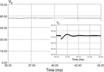
FIGURE 14.125 SL Luo-converter impulse response.
In order to verify the analysis, calculation and simulation results, we constructed a test rig with same conditions. The corresponding test results are shown in Figs. 14.126 and 14.127.
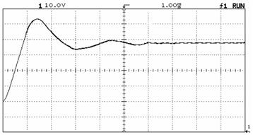
FIGURE 14.126 SL Luo-converter unit-step response (test).
FIGURE 14.127 SL Luo-converter impulse response (test).
Further Reading
1. Luo FL, Ye H. Advanced DC/DC Converters. Boca Raton, Florida 07030, USA: CRC Press LLC; 2004.
2. Luo FL, Ye H, Rashid MH. Digital Power Electronics and Applications. Burlington, Massachusetts 01803, USA: Elsevier Academic Press; June 2005.
3. Luo FL, Ye H. Essential DC/DC Converters. Boca Raton, Florida 07030, USA: Taylor and Francis Group LLC; October 2005.
4. Luo FL. Positive Output Luo-Converters, Voltage Lift Technique. IEE Proceedings on Electric Power Applications. July 1999; vol. 146(No. 4):415–432.
5. Luo FL. Negative Output Luo–Converters, Voltage Lift Technique. IEE Proceedings on Electric Power Applications. July 1999; vol. 146(No. 2):208–224.
6. Luo FL. Double Output Luo–Converters, Advanced Voltage Lift Technique. IEE Proceedings on Electric Power Applications. November 2000; vol. 147(No. 6):618–633.
7. Luo FL. Re–Lift Converter: Design, Test, Simulation and Stability Analysis. IEE Proceedings on Electric Power Applications. July 1998; vol. 145(No. 4):315–325.
8. Luo FL, Ye H, Rashid MH. “Chapter 14: DC/DC Conversion Techniques and Nine Series Luo–Converters” of. In: Rashid MH, ed. Power Electronics Handbook. San Diego, USA: Academic Press; August 2001. [pp. 335–406].
9. Rashid MH. Power Electronics: Circuits, Devices and Applications. Second edition USA: Prentice-Hall; 1993.
10. Mohan N, Undeland TM, Robbins WP. Power Electronics: Converters, Applications and Design. New York: John Wiley & Sons; 1995.
11. Severns RP, Bloom G. Modern DC-to-DC Switchmode Power Converter Circuits. New York: Van Nostrand Reinhold Company; 1985.
12. Kularatna N. Power Electronics Design Handbook. New York: John Wiley & Sons; 1985.
13. Luo FL, Ye H. Advanced Multi-Quadrant Operation DC/DC Converters. Boca Raton, Florida 07030, USA: Taylor and Francis Group LLC; June 2005.
14. Luo FL. Neural Network Control for Synchronous Rectifier DC/DC Converter. Proceedings of the International Conference ICARCV’ 2000. 5–8 December 2000; [CD ROM].
15. Luo FL, Ye H, Rashid MH. Two-Quadrant DC/DC ZCS Quasi-Resonant Luo-Converter. Proceedings of the IEEE International Conference IPEMC’ 2000. 15–18 August 2000; 272–277.
16. Luo FL, Ye H, Rashid MH. Two-Quadrant DC/DC ZVS Quasi-Resonant Luo-Converter. Proceedings of the IEEE International Conference IPEMC’ 2000. 15–18 August 2000; 1132–1137.
17. Luo FL. Negative Output Luo–Converters –Voltage Lift Technique. Proceedings of the Second World Energy System International Conference WES’ 98. 19–22 May 1998; 253–260.
18. Luo FL, Ye H. Ultra-Lift Luo-Converter. IEE-EPA Proceedings. January 2005; vol. 152(No. 1):27–32.
19. Luo FL, Ye H. Positive Output Cascade Boost Converters. IEE-EPA Proceedings. September 2004; vol. 151(No. 5):590–606.
20. Luo FL, Ye H. Positive Output Multiple-Lift Push–Pull Switched-Capacitor Luo-Converters. IEEE-Transactions on Industrial Electronics. June 2004; vol. 51(No. 3):594–602.
21. Luo FL, Ye H. Negative Output Super-Lift Converters. IEEE-Transactions on Power Electronics. September 2003; vol. 18(No. 5):1113–1121.
22. Luo FL, Ye H. Positive Output Super-Lift Converters. IEEE-Transactions on Power Electronics. January 2003; vol. 18(No. 1):105–113.
23. Luo FL, Ye H. Investigation and Verification of a Cascade Double Γ-CL Current Source Resonant Inverter. IEE-EPA Proceedings. September 2002; vol. 149(No. 5):369–378.
24. Luo F, Ye H, Rashid MH. Multiple Quadrant Operation Luo-Converters. IEE-EPA Proceedings. January 2002; vol. 149(No. 1):9–18.
25. Luo FL. Six Self-Lift DC/DC Converters: Voltage Lift Technique. IEEE-Transactions on Industrial Electronics. December 2001; vol. 48(No. 6):1268–1272.
26. Luo FL. Seven Self-Lift DC/DC Converters: Voltage Lift Technique. IEE-EPA Proceedings. July 2001; vol. 148(No. 4):329–338.
27. Luo FL, Ye H, Rashid MH. Four-Quadrant Operating Luo-Converters. Proceedings of the IEEE International Conference PESC’ 2000. 18–23 June 2000; 1047–1052.
28. Luo FL. 42/14 V Two-Quadrant DC/DC Soft-Switching Converter. Proceedings of the IEEE International Conference PESC’ 2000. 18–23 June 2000; 143–148.
29. Luo FL, Ye H. Two-Quadrant Switched Capacitor Converter. Proceedings of the 13th Chinese Power Supply Society IAS Annual Meeting. 15–18 November 1999; 164–168.
30. Luo FL, Ye H. Four-Quadrant Switched Capacitor Converter. Proceedings of the 13th Chinese Power Supply Society IAS Annual Meeting. 15–18 November 1999; 513–518.
31. Luo FL, Ye H, Rashid MH. Switched Capacitor Four-Quadrant Luo-Converter. Proceedings of the IEEE-IAS Annual Meeting, IAS’ 99. 3–7 October 1999; 1653–1660.
32. Luo FL, Ye H, Rashid MH. Switched Inductor Four-Quadrant Luo-Converter. Proceedings of the IEEE-IAS Annual Meeting, IAS’ 99. 3–7 October 1999; 1631–1638.
33. Luo FL. Four-Quadrant DC/DC ZCS Quasi-Resonant Luo-Converter. Accepted for publication by IEE International Conference IPEC’ 2001. 14–19 May 2001.
34. Luo FL. Four-Quadrant DC/DC ZVS Quasi-Resonant Luo-Converter. Accepted for publication by IEE International Conference IPEC’ 2001. 14–19 May 2001.
35. Gao Y, Luo FL. Theoretical Analysis on performance of a 5V/12V Push–Pull Switched Capacitor DC/DC Converter. Accepted for publication by IEE International Conference IPEC’ 2001. 14–19 May 2001.
36. Luo FL, Chua LM. Fuzzy Logic Control for Synchronous Rectifier DC/DC Converter. Proceedings of the IASTED International Conference ASC’ 2000. 24–26 July 2000; 24–28.
37. Luo FL. Luo-Converters –Voltage Lift Technique. Proceedings of the IEEE Power Electronics Special Conference IEEE-PESC’ 98. 14–22 May 1998; 1483–1489.
38. Luo FL. Luo-Converters, A Series of New DC-DC Step-Up (Boost) Conversion Circuits. Proceedings of the IEEE International Conference PEDS’ 97. 26–29 May 1997; 882–888.
39. Luo FL. Re-Lift Circuit, A New DC-DC Step-Up (Boost) Converter. IEE –Electronics Letters. 2 January 1997; vol. 33(No. 1):5–7.
40. Luo FL, Lee WC, Lee GB. Self-Lift Circuit, A New DC-DC Converter. Proceedings of the 3rd National Undergraduate Research Programme (NURP), Congress 97. 13 September 1997; 31–36.
41. Luo FL. DSP-Controlled PWM L-Converter Used for PM DC Motor Drives. Proceedings of the IEEE International Conference SISCTA’ 97. 29–30 July 1997; 98–102.
42. Luo FL. Luo-Converters, New DC-DC Step-Up Converters. Proceedings of the IEE International Conference ISIC-97. 10–12 September 1997; 227–230.
43. Luo FL, Ye H. Synchronous and Resonant DC/DC Conversion Technology, Energy Factor and Mathematical Modeling. Boca Raton, Florida 07030, USA: Taylor and Francis Group LLC; October 2005.
44. Luo FL, Ye H. Chapter 11 (32): D/A and A/D Converters. In: Dorf RC, ed. of Volume 2 of “Electrical Engineering Handbook”. Boca Raton, Florida 07030, USA: CRC Press LLC; September 2004. [0-8493-2774-0].
45. Maksimovic D, Cuk S. A General Approach to Synthesis and Analysis of Quasi-Resonant Converters. IEEE Transactions on PE. January 1991; vol. 6(No. 1):127–140.
46. Middlebrook RD, Cuk S. Pasadena, CA: TESLAco; 1981.
47. Liu Y, Sen PC. New Class-E DC-DC Converter Topologies with Constant Switching Frequency. IEEE-IA Transactions. July/August 1996; vol. 32(No. 4):961–969.
48. Redl R, Molnar B, Sokal NO. Class-E Resonant DC-DC Power Converters: Analysis of Operations, and Experimental Results at 1.5 MHz. IEEE Transactions, Power Electronics. April 1986; vol. 1:111–119.
49. Kazimierczuk MK, Bui XT. Class-E DC-DC Converters with an Inductive Impedance Inverter. IEEE Transactions, Power Electronics. July 1989; vol. 4:124–135.
50. Massey R. P. and Snyder E. C. “High Voltage Single-Ended DC-DC Converter” IEEE PESC, 1977 Record, pp. 156–159.
51. Jozwik JJ, Kazimerczuk MK. Dual Sepic PWM Switching-Mode DC/DC Power Converter. IEEE Transactions on Industrial Electronics. 1989; vol. 36(No. 1):64–70.
52. Martins D. C. “Application of the Zeta Converter in Switch-Mode Power Supplies” Proc. of IEEE APEC’ 93, USA, pp. 214–220.
53. Kassakian JG, Wolf H-C, Miller JM, Hurton CJ. Automotive electrical systems, circa 2005. IEEE Spectrum. August 1996; 22–27.
54. Wang J., Dunford W. G., and Mauch K. “Some Novel Four-Quadrant DC-DC Converters” Proc. Of IEEE-PESC’ 98, Fukuoka, Japan, pp. 1475–1482.
55. Luo FL. Double Output Luo-Converters. Proceedings of the IEE International Conference IPEC’ 99. 24–26 May 1999; 647–652.
56. Ye H, Luo FL. Luo-Converters, A Series of New DC-DC Step-Up Conversion Circuits. International Journal <Power Supply Technologies and Applications>. April 1998; vol. 1(No. 1):30–39 [Xi’an, China].
57. Ye H, Luo FL. Advanced Voltage Lift Technique –Negative Output Luo-Converters. International Journal <Power Supply Technologies and Applications>. August 1998; vol. 1(No. 3):152–168 [Xi’an, China].
58. Luo FL. Negative Output Luo-Converters –Voltage Lift Technique. Proceedings of the Second world energy system International Conference WES’ 98. 19–22 May 1998; 253–260.
59. Luo FL. Luo-Converters –Voltage Lift Technique. Proceedings of the IEEE Power Electronics Special Conference IEEE-PESC’ 98. 14–22 May 1998; 1483–1489.
60. Luo FL, Ye H. Two-Quadrant DC/DC Converter with Switched Capacitors. Proceedings of the International Conference IPEC’ 99. 24–26 May 1999; 641–646.
61. Midgley D, Sigger M. Switched-capacitors in power control. IEE Proc.. July 1974; vol. 121:703–704.
62. Cheong SV, Chung H, Ioinovici A. Inductorless DC-DC Converter with high Power Density. IEEE Trans. on Industrial Electronics. April 1994; vol. 41(No. 2):208–215.
63. Midgley D, Sigger M. Switched-capacitors in power control. IEE Proc.. July 1974; vol. 121:703–704.
64. Chung H, Hui SYR, Tang SC. A low-profile Switched-capacitor-based DC/DC Converter. Proc. of AUPEC’ 97. October 1997; 73–78.
65. Ngo KDT, Webster R. Steady-state Analysis and Design of a Switched-Capacitor DC-DC Converter. IEEE Transactions on ANES. January 1994; vol. 30(No. 1):92–101.
66. Harris WS, Ngo KDT. Power Switched-Capacitor DC-DC Converter: Analysis and Design. IEEE Transactions on ANES. April 1997; vol. 33(No. 2):386–395.
67. Tse CK, Wong SC, Chow MHL. On Lossless Switched-Capacitor Power Converters. IEEE Trans. on PE. May 1995; vol. 10(No. 3):286–291.
68. Luo FL, Ye H. Energy Factor and Mathematical Modeling for Power DC/DC Converters. IEE-EPA Proceedings. March 2005; vol. 152(No. 2):191–198.
69. Mak OC, Wong YC, Ioinovici A. Step-up DC Power Supply Based on a Switched-capacitor Circuit. IEEE Trans. on IE. February 1995; vol. 42(No. 1):90–97.
70. Mak OC, Ioinovici A. Switched-capacitor Inverter with High Power Density and Enhanced Regulation Capability. IEEE Trans. on CAS-I. April 1998; vol. 45(No. 4):336–347.
71. Luo FL, Ye H. Switched Inductor Two-Quadrant DC/DC Converter with Fuzzy Logic Control. Proceedings of IEEE International Conference PEDS’ 99. 26–29 July 1999; 773–778.
72. Luo FL, Ye H. Switched Inductor Two-Quadrant DC/DC Converter with Neural Network Control. Proceedings of IEEE International Conference PEDS’ 99. 26–29 July 1999; 1114–1119.
73. Liu KH, Lee FC. Resonant Switches –A Unified Approach to Improved Performances of Switching Converters. International Telecommunications Energy Conference (INTELEC) Proc.. 4–7 November 1984; 344–351.
74. Liu KH, Lee FC. Zero-Voltage Switching Techniques in DC/DC Converter Circuits. Power Electronics Specialist’s Conf. (PESC) Record. June 1986; 58–70.
75. Martinez ZR, Ray B. Didirectional DC/DC Power Conversion Using Constant-Frequency Multi-Resonant Topology. Applied Power Electronics Conf. (APEC) Proc.. 13–14 February 1994; 991–997.
76. Pong MH, Ho WC, Poon NK. Soft Switching Converter with Power Limiting Feature. IEE-EPA Proceedings. January 1999; vol. 146(No. 1):95–102.
77. Gu WJ, Harada K. A Novel Self-Excited Forward DC-DC Converter with Zero-Voltage-Switched Resonant Transitions using a Saturable Core. IEEE-PE Transactions. March 1995; vol. 10(No. 2):131–141.
78. Cho JG, Sabate JA, Hua G, Lee FC. Zero-Voltage and Zero-Current-Switching Full Bridge PWM Converter for High Power Applications. IEEE-PE Transactions. July 1996; vol. 11(No. 4):622–628.
79. Poon NK, Pong MH. Computer Aided Design of a Crossing Current Resonant Converter (XCRC). Proceedings of IECON’ 94. 5–9 September 1994; 135–140.
80. Kassakian JG, Schlecht MF, Verghese GC. Principles of Power Electronics. New York: Addison-Wesley; 1991 [p. 214].